Note: Descriptions are shown in the official language in which they were submitted.
CA 02767241 2012-01-04
WO 2011/004190 PCT/GB2010/051118
Method of Forming a Photonic Crystal Material
Field of the Invention
The present invention relates to improvements in methods of forming films of
photonic crystal material having an optical effect.
Background to the Invention
Photonic crystals are structured optical materials in which the refractive
index
varies periodically in two or preferably three dimensions. These materials
exhibit
a range of interesting optical effects when subject to electromagnetic
radiation of
a wavelength comparable to the spatial modulation of the refractive index.
Bragg
reflection may occur over a range of wavelengths that depend on the direction
of
incidence/propagation and the periodicity of refractive index variation. This
gives rise to photonic `energy gaps' that are analogous to the electronic band
gaps in semiconductors. Typically, electromagnetic waves within a certain
frequency range cannot propagate in particular directions within the crystal,
and
incident electromagnetic radiation at these wavelengths is consequently
reflected. It is the presence of such partial photonic band gaps that gives
rise to
the shimmering colours observed in opal gemstones.
In general there is a complex dependence on the wavelength, direction of
propagation and polarisation that dictates which electromagnetic waves may
propagate within the photonic crystal and those that are otherwise reflected.
However, if the modulation in refractive index is sufficiently strong,
propagation
of certain frequencies can be forbidden for any crystalline direction, and a
complete photonic band gap arises. In this case light is prevented from
propagating within the crystal in any direction, and the material acts as an
ideal
reflector such that all light of a wavelength within the band gap range is
perfectly
reflected irrespective of the incident direction.
There exist two well-documented methods of fabricating structures with the
necessary highly ordered variation in refractive index - microfabrication and
self-
1
CA 02767241 2012-01-04
WO 2011/004190 PCT/GB2010/051118
assembly. Due to the complexity of microfabrication considerable effort has
been devoted to investigating self-assembling systems comprised of submicron
three-dimensional arrays of dielectric spheres. Such photonic crystals are
formed by allowing a colloidal suspension of identically sized spheres to
settle
slowly under the influence of gravity or by the application of an external
force
such that the spheres are encouraged to order. One example is the fabrication
of synthetic opal structures where uniformly sized sub-micron silica spheres
are
organised through a sedimentation process into a face-centred cubic crystal
structure. Another example is the use of polymer "core-shell" particles. Here
a
core of a first polymer is surrounded (sometimes with an intermediate layer)
by a
shell of a second polymer. A photonic crystal material is formed by the
heating of
the particles such that the shell melts and forms a matrix within which the
core
particles arrange into a regular structure. This example is of particular
interest
because of the polymeric nature of the photonic crystal material which
provides
the potential for a range of new applications.
There is an ongoing desire to improve the techniques used in producing such
photonic crystal structures with a view to providing substantial quantities of
the
materials at a low cost and in a form suitable for later applications. For
this
reason there is considerable interest in the production of photonic materials
as
films which may then be incorporated within or applied to a product.
Unfortunately a significant problem exists because the fabrication methods
inherent within film production are not always amenable to the preservation of
the photonic structure of the materials. These effects are further amplified
as the
thickness of the films is decreased. The result is that film production
techniques
cause the reduction or even complete loss of any optical effects exhibited by
the
photonic crystal material. An objective of the invention is to address this
problem
so as to provide films of photonic crystal material in which a strong optical
effect
is present.
Further challenges exist in the production of such films on an industrial
scale.
One such challenge is the production of homogeneous optical properties such
that all of the film can be observed to produce a similar optical effect.
Known
processing techniques can cause variations within the photonic crystal
structure
as a result of localised strains. These can result in films having significant
2
CA 02767241 2012-01-04
WO 2011/004190 PCT/GB2010/051118
variations in optical properties in different regions, which increases wastage
and
costs. Furthermore, other challenges exist in the provision of films which may
be
readily handled, particularly in the case of films which are thin (for example
under 100 micrometres) where the film strength may be low or surface
stickiness
may prevent ease of use.
Summary of the Invention
In accordance with a first aspect of the invention we provide a method of
forming
a film of photonic crystal material, comprising:-
providing a material capable of having a photonic crystal structure;
performing a first process upon the material which causes deformation of the
material so as to form a film in which incident light received by the material
is
selectively reflected or transmitted to generate a first optical effect in the
film;
and
performing a second process upon substantially all of the film which applies a
shear stress to the film, thereby causing a change in the material structure
so as
to generate a second optical effect in the film, different from the first
optical
effect, in response to incident light.
We have therefore overcome the problems caused by known film production
techniques in generating films of photonic crystal materials by the
application of
a second process which applies a shear stress to the film. The shear stress is
typically applied by the use of dissimilar forces in opposed surfaces of the
film.
Thus the forces may be in a similar direction and of a different magnitude or
may
be in opposed directions and of either a similar or dissimilar magnitude. It
is also
contemplated that the respective forces may not be aligned in either the same
or
opposed directions. The shear forces are therefore preferably applied in
directions lying substantially within or parallel to planes defining the
surfaces of
the film. It is contemplated that the application of the shear stress by the
second
process may include a simultaneous application of a compressive stress. In
applying the shear stress to ensure substantially all areas of the film
surface are
3
CA 02767241 2012-01-04
WO 2011/004190 PCT/GB2010/051118
processed it will be understood that the magnitude of the shear stress is
typically
in excess of any compressive or indeed tensile stresses applied by the same
process. Typically therefore, the primary effect of the application of the
shear
stress is to cause local rearrangement of the particles within the film so as
to
enhance its photonic crystallinity. Thus, typically the second process does
not
substantially affect the thickness of the film. Indeed the process may induce
a
shear strain which causes a minor amount of elongation.
In general, the shear stress is applied to substantially all of the film in
each of its
1o two major dimensions (other than the thickness). Therefore the resultant
film
provides a similar second optical effect at all observed locations across its
surface. It is expected that in some cases, some rearrangement of the material
may occur throughout the film thickness and therefore substantially all of the
film
may be treated in each of its three dimensions. However, this is not
essential,
particularly in thicker films where regions closer to the surfaces may be
responsible for generating much of the second optical effect and central
regions
of the film thickness may remain substantially unaffected. The invention
contemplates the simultaneous application of the shear stress to substantially
all
of the film by the second process. However, it will be preferred in many cases
to
apply the shear stress to a local processing region which is passed along the
length of the film (typically by moving the film). This is beneficial to
longer
lengths of film such as in the case of semi-continuous or continuous
processing.
The first optical effect, which is present prior to the application of the
second
process, is intended to be interpreted broadly as including any optical
effect. In
essence the first optical effect may therefore be either a photonic effect or
a non-
photonic effect and include the natural appearance of the material prior to
any
form of film processing. Depending upon the material it may however include a
photonic effect or other optical effect caused by the first process, including
an
optically variable effect.
Although the second optical effect may be a photonic effect which is not
optically
variable (that is, it is not dependent upon the viewing or illumination
position)
such as broadband reflection, it is preferably an optically variable effect.
The
second effect may therefore be an entirely distinct effect from that of the
first
4
CA 02767241 2012-01-04
WO 2011/004190 PCT/GB2010/051118
effect. In other cases it may be an enhanced effect which produces a higher
intensity response to the incident radiation and yet produces a similar
spectrum
as a function of viewing and illumination position. In each case the second
effect
is typically caused by an increase in photonic crystalline order and, where an
enhanced effect is produced, this represents an increase in order within
respect
to the degree of ordering already present as a result of the first effect.
We note here that reflected light in the context of the present invention
includes
both specularly reflected light and scattered light. It should also be noted
that
1o various types of photonic crystals may be used to achieve the present
invention,
and the term "photonic crystal" is intended to include quasi-crystals that
exhibit
this effect, as well as more conventional ordered "non-quasi" photonic
crystals.
The optical effects of the invention are not intended to be limited to operate
only
in the wavelengths observable by the human eye. Thus, in addition to visible
light it is intended that the invention may be practised at other non-visible
wavelengths including ultra-violet and infra-red regimes within the
electromagnetic spectrum. One or each of the first and second optical effects
may be in the visible or non-visible parts of the spectrum. When the incident
light
is produced by a white light (broad wavelength band) source, preferably at
least
the second optical effect is a colour effect. Whilst the first and second
effects are
preferably observed as reflective effects, transmissive effects are also
contemplated.
With reference to the film itself, typically the film has a maximum dimension
in an
elongate direction, an intermediate dimension in a width direction that is
substantially normal to the elongate direction, and a minimum dimension in a
thickness direction that is substantially normal to each of the elongation and
width directions. In this case the second optical effect is present across
substantially the full width of the film in the width direction. Similarly the
second
optical effect is present along substantially the full length of the film in
the
elongate direction, which provides that substantially all of the film area
exhibits
the second optical effect.
5
CA 02767241 2012-01-04
WO 2011/004190 PCT/GB2010/051118
The film may be produced in batches, in which case each batch may provide a
long length of film, for example tens of metres in length. In order to produce
the
film most efficiently it is preferably produced as a continuous film. For
example,
provided a supply of materials is assured for generating the film, it may be
continuously produced and processed, followed by spooling and cutting
downstream, prior to or subsequent to any further processing.
The method is, in principle, not limited to any particular film thicknesses,
although it finds particularly beneficial application where the thickness of
the film
is 100 micrometres or less. Most preferably the film has a thickness of 40
micrometres or less. Thin films of 100 micrometres or less are particularly
beneficial for many security applications since they may be incorporated into
documents of value and thereby provide new optical effects which are extremely
difficult to counterfeit.
A number of different techniques may be used for producing the film according
to the first process. Where the films are polymeric, the production methods
include rolling, calendaring, film blowing or flat-film extrusion.
In the production of a strong and homogeneous second optical effect it is
beneficial to ensure that the film has a smooth surface prior to application
of the
second process. This may be achieved by performing a calendaring process on
the film before performing the second process (and therefore as part of the
first
process or as an intermediate process). Typically such a calendaring process
applies a pressure to the film of between 50 and 200 bar (about 5 to 20 MPa)
and at a temperature of 80 to 120 Celsius. Once the film has been processed to
produce the second optical effect it is beneficial to ensure the long-term
stability
of the optical effect. This may be achieved by a process of cross-linking.
Such
cross-linking may be achieved by the provision of additives within the film
material which are responsive to stimulation by heat or ultra-violet light. It
is
preferred that thermal cross-linking is performed since the second process is
typically performed at an elevated temperature which may simplify the
processing required. Cross-linking may also be used to reduce any surface
stickiness of the films.
6
CA 02767241 2012-01-04
WO 2011/004190 PCT/GB2010/051118
The photonic crystal film resulting from the process may be provided in a
number of forms, for example as a self-supporting layer. Alternatively, it may
be
supported by a substrate or carrier layer to which it is mounted directly or
indirectly (through one or more further layers). The substrate or the carrier
layer
may take the form of a polymeric layer.
The method preferably includes applying a cover film to one or each of the
opposing surfaces of the film before the performance of the second process.
The use of one or more cover films provides benefits in that they protect the
photonic crystal film for example from surface damage due to the use of
rollers
and guides. They also may provide mechanical support to the film, providing
ease of handling. Cover films provide further convenience where the photonic
crystal film surface is tacky which may otherwise cause damage when handling.
In addition to each of these benefits, one further important and surprising
benefit
is that the one or more cover films may be used within the second process to
achieve the application of the shear stress. Thus, the shear stress of the
second
process is preferably applied to at least one of the said cover films. When
the
cover films are used within the second process they serve to equalise the
shear
stress of the processed area such that the stress may be applied evenly. The
result of this is that the second optical effect is extremely homogeneous and
applied evenly to all parts of the photonic film surface. It is preferred that
the
cover films are applied to each of the opposing surfaces. The effect of this
is that
the second process causes the displacement of one cover film with respect to
the other in the elongate direction of the film. One or each cover film may
also
function as a substrate or carrier layer.
Depending upon the type of photonic crystal material used for the film, the
processing may be performed at ambient temperature. However, particularly in
the case of polymer films, each of the first and second processes are
preferably
performed at respective first elevated and second elevated temperatures
whereby, between the application of the first and second processes, the
temperature of the material remains substantially at or above the second
elevated temperature. In general each of the first and second elevated
temperatures are arranged to be in excess of the glass transition temperature
of
a polymer matrix component of the photonic crystal material.
7
CA 02767241 2012-01-04
WO 2011/004190 PCT/GB2010/051118
It will be understood that the method is not limited to any particular type of
photonic crystal material, particularly since it is not required that a
photonic
crystalline structure results as an output of the first process, although
preferably
partial photonic crystallinity is achieved. The method is particularly suited
to
polymeric materials and preferably the photonic material comprises a
polyethylacrylate matrix containing spheres of cross-linked polystyrene.
The first process may include an extrusion process in which a film is produced
as a result of forcing the material through an extrusion die with a cross
section
being similar to that of the film. However, it has been found that it is not
necessary for a film itself to be extruded and therefore other non-film cross-
sections may be produced in which case the extrusion may be thought of as a
first sub-process. In this case a further sub-process which is part of the
first
process, converts the extrudate into a film, an example of such a process
being
a rolling process.
A number of different second processes are contemplated by the present
invention. A preferred example is that the shear stress of the second process
is
applied by passing the material over at least one sharp edge. Where heating of
the film is a requirement of the second process, then the second process may
be performed within a heated chamber.
In the case of an edge, it is beneficial to ensure a significant directional
change
of the film at the point of contact with the edge. It is preferred that the
respective
parts of the film, upstream of the edge, passing over the edge, and downstream
of the edge, define an angle of 120 degrees or less, wherein the said angle is
subtended by the edge. A potential problem with small angles is to provide
smooth flow of the film over the edge surface. This may be addressed with the
provision of a low friction material at the edge, such as a
polytetrafluoroethylene.
The edge may also be heated, for example to a temperature of 200 degrees
Celsius.
It is important that the film remains urged against the edge in order to apply
the
shear stress. Rollers may be used to grip the film upstream and downstream of
8
CA 02767241 2012-01-04
WO 2011/004190 PCT/GB2010/051118
the edge in order to control the shear stress applied. When the second process
is applied at an elevated temperature, the upstream rollers may be heated.
Furthermore, regardless of whether heated rollers are used upstream, the
cooling of the film following the second process may be performed using one or
more cooled rollers.
Each of the first and second optical effects may be modified or enhanced by
the
use of additional additives within the material itself. The material of the
film may
further comprise an optically absorbent material within the film crystal
structure
itself. The inclusion of such an optically absorbent material can be used to
enhance the optical effect to an observer, or used to modify the optical
effect by
the use of for example absorbent materials that are selectively absorbent at
the
wavelengths of light used. Dyes or inks may be used for this purpose.
It has been reported in the scientific literature, (see Optics Express, Vol.
15, No.
15, Page 9553-9561, 23rd July 2007), that nanoparticles can be introduced into
the matrix of a photonic crystal in order to change or enhance the observed
colours, colourshifts and tolerance on illumination angle.
In addition or as an alternative to any optically absorbent additives, the
optical
properties according to the second optical effect may be further modified or
enhanced by the use of nanoparticles positioned within the crystal structure
of
the film, preferably at interstitial sites. The nanoparticles may be
distributed
substantially uniformly through the film such that each part of the film
exhibits
substantially the same optical effect. Alternatively the nanoparticles may be
distributed inhomogeneously through the film such that different parts of the
film
exhibit a substantially different optical effect. Thus the nanoparticles may
be
distributed according to a concentration gradient, for example in the through-
thickness direction where a relatively high concentration at one surface
reducing
to a relatively low concentration at the opposing film surface. The
concentration
gradient may also be arranged to be symmetrically distributed about the centre
of the film thickness (for example higher or lower at the centre with respect
to
one or each surface).
9
CA 02767241 2012-01-04
WO 2011/004190 PCT/GB2010/051118
Preferably the size of the nanoparticles is selected such that they sit within
the
interstitial sites of the crystal lattice. The nanoparticles enhance resonant
scattering events that occur within the photonic crystal giving rise to strong
structural colours.
For example the incorporation of carbon nanoparticles less than 50nm in
diameter into a material comprising polystyrene spheres with a sphere size of
200nm in a polyethlyacrylate matrix, enhances the resonant scattering of the
photonic crystal and dramatically alters the appearance of the photonic
crystal
1o film from one with a weakly coloured opalescence appearance to an intensely
coloured green film. In this way the first optical effect may be a strong
photonic
optical effect, whereas in the absence of the nanoparticles such an effect may
be only weak or non-photonic in nature. The second optical effect may of
course
also be enhanced or modified with respect to the second optical effect in the
absence of the nanoparticles.
The use of the nanoparticles therefore provides a key advantage in that
intense
colours are observed and there is an increased tolerance on illumination angle
such that the observed colour is no longer as dependent on the position of the
light source. In another example magnetite nanoparticles can be incorporated
to
generate a magnetic machine-readable colourshifting film.
It is preferred that when the polymeric photonic crystal film is produced by
an
extrusion process, the nanoparticles are added to the polymer reservoir prior
to
extrusion. The particles may be made from material which is orientable in an
electric, magnetic or electromagnetic field. In this way, alignment of the
particles
may be effected by selective application of that specified field to the
photonic
crystal film prior to any final cross-linking step in the film production.
Nano-photoluminescent particles such as quantum dots may be added to create
a novel photoluminescence effect which may be used as a security feature. For
example PbS nanoparticles can be added to produce luminescent films. It has
been shown in the scientific literature (Nature Materials Volume 5 March 2006
Page 179) that embedding quantum dots in a photonic crystal results in
suppression of luminescence if the emission frequency falls within the band
gap
CA 02767241 2012-01-04
WO 2011/004190 PCT/GB2010/051118
of the photonic crystal. If the position of the photonic band gap varies
according
to the direction of the incident light relative to the crystal orientation,
such that it
overlaps or crosses through the photoluminescence peak of the embedded
emitter, suppression/enhancement of emission and dynamic modification of the
luminescence lifetimes may occur creating an effect where the fluorescence or
phosphorescence is switched on or off by simply rotating the device relative
to
the incident radiation.
The first and/or second optical effects may be characterised using techniques
such as spectroscopy, for example reflective or transmissive. For example, the
second optical effect may be characterised by a peak in the transmissive
absorbance spectrum taken through the film. The peak may exhibit a shift in
wavelength as a function of rotation of a line defining an emitter and
detector,
the line passing through the film and rotating about a rotation axis lying
within
the plane of the film. Typically such a rotation axis is aligned parallel to
the
direction of elongation of the film or perpendicular to that direction.
Further processing methods may be performed upon the film, such as the
application of a third process to the film so as to modify the structure of
the material
in one or more regions. For example the third process may provide one or more
regions have an at least approximately opal-like structure having a reduced
degree
of crystal ordering with respect to the rest of the film (having an opal-like
structure).
Thus, the third process may be a deformation process which causes disordering
of
the material structure in the one or more regions, either by the displacement
or the
deformation of the objects (such as spheres) which make up the crystal
structure.
The third process may be an embossing process, wherein the embossing takes
place during an intaglio printing process and is carried out using an intaglio
plate.
Another example third process is where the photonic crystal structure of the
film
comprises a number of objects of similar geometry, formed from a first
material,
located within a matrix of a second material, different from the first. The
third
process of the method may comprise removing the objects of the first material
from
the photonic crystal material when arranged in an opal-like structure, so as
to form
an inverse opal-like structure. Alternatively the whole film may be treated in
this
manner, rather than the application to specific regions. The objects may be
removed
by applying a solvent to the objects. Such a solvent may be applied by one or
more
11
CA 02767241 2012-01-04
WO 2011/004190 PCT/GB2010/051118
of the processes of: immersing the material in a bath of solvent or printing
the
solvent onto the photonic crystal material. Furthermore, prior to the removal
of the
objects, an area of the material may be protected by the application of a
mask. As a
further process, the method may comprise applying a further deformation
process to
part of the inverse opal-like structure.
A second aspect of the invention comprises a film made in accordance with the
first
aspect of the invention. Films produced according to the method of the present
invention find numerous applications. One such application is the
incorporation of
the film into a security device. Thus in accordance with a third aspect of the
invention we provide a security device incorporating a film produced in
accordance
with the method of the first aspect. Such a security device may include a
number of
additional layers or elements. For example the security device may be provided
with
an adhesive layer upon one or each outer surface thereof. It may also comprise
a
scattering layer to increase the visibility of optical effects at wider
viewing angles. An
optically absorbent material may also be provided as one or more layers
applied to
the device. The absorbent material may be selectively absorbent at light
wavelengths and may be provided as an ink or dye.
The security device may further comprise a metallised layer. Preferably such a
layer
is selectively demetallised at a number of locations. In addition the device
may
further comprise a layer of resist upon the metallised layer. The metallised
layer
and/or the layer of resist is preferably arranged as indicia. Such layers with
or
without indicia may be visible from the same side of the photonic crystal that
receives the light, or from the reverse side. Transmissive viewing of the
layers is
also contemplated.
It is also preferred that the device is arranged to be machine-readable. This
may be
achieved in a number of ways. For example at least one layer of the device
(optionally as a separate layer) or the photonic crystal itself may further
comprise
machine-readable material. Preferably the machine-readable material is a
magnetic
material, such as magnetite. The machine-readable material may be responsive
to
an external stimulus. Furthermore, when the machine-readable material is
formed
into a layer, this layer may be transparent.
12
CA 02767241 2012-01-04
WO 2011/004190 PCT/GB2010/051118
Typically the device is formed from a number of different layers and the
device is
adapted to be substantially planar. The device may be adapted to be observed
from
first and second opposing sides. In order to enhance the security features of
the
device, the surface of the photonic crystal film may be embossed with raised
structures and/or overprinted. A latent image may also be formed which is
selectively visible according to the viewing angle. Other security features
may be
included within the device, for example the security device may further
comprise a
hologram.
The security device may be used in many different applications, for example by
attachment to articles such as objects of value. The security device may take
various different forms for use with such articles, these including a security
thread, a
security fibre, a security patch, a security strip, a security stripe or a
security foil as
non-limiting examples.
In accordance with a fourth aspect of the invention there is provided an
article
comprising one or more security devices in accordance with the third aspect of
the
invention. Preferably, the security devices are adhered to or substantially
contained
within the article. Such articles include security documents in the form of a
bank
note, driving licence, passport, identity card, credit or debit payment cards,
fiscal
stamp, cheque, postal stamp, certificate of authenticity, brand protection
article,
bond or payment voucher. Other articles include general packaging and
particularly
packaging for pharmaceuticals or other items whose authenticity is desired to
be
assured.
The security device may therefore be attached to a surface of such an article
or it
may be embedded within the article so as to provide photonic crystal surfaces
for
receiving incident light on one or each of opposing faces of the article. The
device
may be embedded within a window so as to provide crystal surfaces for
receiving
incident light on each of opposing faces of the document. Each of these
features is
particularly beneficial for security document applications.
In accordance with a fifth aspect of the invention there is provided apparatus
for
forming a film of photonic crystal material, comprising:-
13
CA 02767241 2012-01-04
WO 2011/004190 PCT/GB2010/051118
a film generator adapted to perform a first process upon the material which
causes
deformation of the material so as to form a film in which incident light
received by
the material is selectively reflected or transmitted to generate a first
optical effect in
the film; and
a shearing processor adapted to perform a second process upon substantially
all of
the film which applies a shear stress to the film, thereby causing a change in
the
material structure so as to generate a second optical effect in the film,
different from
the first optical effect, in response to incident light.
Thus the film generator may take the form of any of the apparatus discussed
herein
for performing the first process, for example an extruder. The shearing
processor
may therefore comprise apparatus including one or more sharpened edges or any
other apparatus for performing the shearing function. Preferably the apparatus
according to the fifth aspect is adapted in use to perform the method of the
first
aspect of the invention and may include further processing apparatus to
generate
films, security devices, articles and documents according to the other aspects
of the
invention.
Brief Description of the Drawings
Some examples of method of forming films of photonic crystal material are now
described with reference to the accompanying drawings, in which:-
Figure 1 is a flow diagram illustrating the example method;
Figure 2 is a schematic diagram of apparatus for performing the method;
Figure 3 shows an example colour enhancement unit;
Figure 4 shows two measurement regimes for use with a transmissive
spectrometer;
Figures 5a and 5b show absorption spectra of the example films in parallel and
normal configurations after extrusion;
Figures 6a and 6b show corresponding spectra of the example films following
the shearing process;
Figure 7 shows a comparison between the spectra before and after the colour
enhancement process;
14
CA 02767241 2012-01-04
WO 2011/004190 PCT/GB2010/051118
Figures 8a and 8b show reflection spectra illustrating the Bragg peak with a
black and white background respectively;
Figure 9 shows the effect of off-gloss angles;
Figure 10 shows a first example of a security document in plan view;
Figure 11 shows the first example document in section;
Figure 12 shows an example security document having a windowed thread;
Figure 13 shows the second example document in section;
Figure 14 shows a third example document in section;
Figure 15a shows a fourth example document including demetallised characters;
Figure 15b shows a machine-readable version as a fifth example document;
Figure 16 shows a sixth example document having a transparent region;
Figure 17a shows a seventh example document in section;
Figure 17b shows a machine-readable version of the seventh example
document;
Figures 18a to 18d show an eighth example document having an aperture in a
paper substrate when viewed from different angles;
Figures 19a and 19b show a ninth example document using hot stamped
regions when viewed from different angles;
Figure 20 shows an embossed tenth example document;
Figure 21 shows an eleventh example document in section having gaps in the
photonic film; and,
Figure 22 shows a flow diagram of an example method of fabricating a security
device.
Details of Preferred Examples
We now describe a method, together with suitable apparatus, for producing a
thin film of photonic crystal material which exhibits a strong angularly
dependent
colour effect. We then describe the use of the film in various example
applications related to security devices and documents.
Materials
The present invention is not intended to be limited by the specific use of
certain
materials and this example now illustrates one practical implementation. As
has
been explained known methods of forming photonic crystal materials include
micro fabrication and self-assembly. Due to the complexities of micro
fabrication
CA 02767241 2012-01-04
WO 2011/004190 PCT/GB2010/051118
processes, it has become preferred in the art to use self-assembly. Synthetic
opal structures can be formed by such a mechanism where uniformly sized sub-
micron siliceous spheres are organised through a sedimentation process in a
face-centred cubic crystal structure. Likewise, inverse-opal structures can
also
be formed by the dissolution of the siliceous spheres. Whilst the present
invention can in principle be implemented with such materials, it is preferred
that
the materials of the films exhibiting photonic crystal structure are based
upon
polymer technology and it is this technology which is utilised in the present
example. Polymeric based photonic crystal materials are particularly suitable
for
1o the present invention and preferably these comprise polymeric materials for
each of the matrix and the "spheres". Thus the crystal may be formed from
spheres of a first material and the matrix of a second material, each being
polymeric in nature and exhibiting a different respective refractive index.
Whilst
the discussion herein focuses upon the provision of "spheres", in principle
however many other shapes may be used including ellipsoidal, cylindrical and
other geometries.
Materials suitable for forming the spheres are preferably single polymer or
copolymer materials. Examples of these include both polymers and copolymers
of polymerisable unsaturated monomers, and polycondensates and
copolycondensates of monomers containing at least two reactive groups. For
example such groups include high-molecular-weight aliphatic,
aliphatic/aromatic
or fully aromatic polyesters, polyamides, polycarbonates, polyureas and
polyurethanes, but also amino and phenolic resins, such as, for example,
melamine-formaldehyde, urea-formaldehyde, phenol-formaldehyde
condensates. Materials suitable for forming the matrix include polymers and
copolymers of polymerisable unsaturated monomers and also of the
polycondensates and copolycondensates of monomers having two or more
reactive groups, e.g., high-molecular-weight aliphatic, aliphatic/aromatic or
wholly aromatic polyesters and polyamides, but also of the amino and phenolic
resins such as melamine-formaldehyde, urea-formaldehyde and phenol-
formaldehyde condensates.
It is preferable to use polymeric materials for each of the matrix and the
spheres
since these are together more easily formed into films. The polymer materials
for
16
CA 02767241 2012-01-04
WO 2011/004190 PCT/GB2010/051118
each of the matrix and the spheres may be selected to maximise the respective
refractive index difference. Typically such a refractive index difference
should be
at least 0.001, more preferably greater than 0.01 and even more preferably
greater than 0.1. Non-polymeric materials are also envisaged for the spheres
and/or the matrix and they may comprise inorganic or metallic materials or a
hybrid composite.
One convenient method for reproduction of photonic crystal materials having
both a matrix and particles formed from polymers is the use of core-shell (CS)
particles. As a typical example, each core-shell particle may consist of a
highly
cross-linked polystyrene core, coated with a cross-linked
polymethylmethacrylate (PMMA) interlayer and a soft, meltable, shell of
polyethylacrylate (PEA). The refractive index difference in this case is about
0.12
between the core and the shell. The advantage of using PEA is due to its low
glass transition temperature of -15 C. The PMMA interlayer is useful for
providing sufficient grafting of the PEA shell chains on the core via the
reactive
cross-linking molecule allylmethacrylate (ALMA). However, such materials when
formed into thin films do encounter some problems, particularly in that the
film
strength may be too low and the surface of the film is sticky or tacky.
Providing an additional degree of cross-linking increases the elasticity and
reduces the stickiness. Taking the above material as a starting point, a
number
of modifications were applied to the chemistry. Firstly copolymerisation of
the
ethylacrylate with isobutylmethacrylate increased the glass transition
temperature of the shell polymer slightly. Secondly, the shell polymer was
slightly pre-crosslinked during the emulsion polymerisation process by which
the
core-shell particles are formed. Thirdly, OH-functionality was introduced into
the
shell polymer to allow thermal crosslinking. Furthermore, the crosslinked
interlayer was modified by changing the material from PMMA to
polyethylacrylate.
Three different example core-shell particle chemistries provided high quality
core-shell particles according to the above. These were: Sample 1 (denoted
CS322) had a polystyrene core containing 10% of butanediol diacrylate (BDDA),
a PMMA interlayer with 10% ALMA, surrounded by a PEA outer shell containing
17
CA 02767241 2012-01-04
WO 2011/004190 PCT/GB2010/051118
2% of hydroxyethyl methacrylate (HEMA); Sample 2 (denoted CS354) had a
polystyrene core containing 10% of butanediol diacrylate (BDDA), a PEA
interlayer with 10% ALMA, surrounded by a PEA outer shell containing 3% of
hydroxyethyl methacrylate (HEMA). Sample 3 (denoted CS355) had a similar
core and interlayer to Sample 2, and a modified outer shell of 71.72% Ethyl
Acrylate, 25% iso-Butyl Methacrylate (iBMA), 3% HEMA and 0.18% Diallyl
Phthalate (DAP). Each had a peak particle size distribution of about 300 nm.
The particle size distribution was investigated by hydrodynamic fractionation.
Use of a particle size distribution analyser confirmed the standard deviation
of
1o the particle size diameter to be less than 10%.
The batches for use in the production of the films were prepared by
coagulation
of the aqueous lattice in methanol, saturated with sodium chloride, followed
by
filtering and drying in a convective oven at 45 C for 2 days. The dried
polymer
was then milled with dry ice prior to being provided to the extruder to be
discussed below. An alternative technique would be to use spray drying
including the use of additives to prevent coagulation.
Powders produced by either of these techniques may then be used and mixed
with pigments and any other additives, within the melt formed by an extruder.
The use of pigments and other additives during general extrusion processes is
known within the polymer processing industry.
Having given examples of the initial materials for the production of the
photonic
crystal film, we now describe the method itself. With reference to the flow
diagram of Figure 1 and system diagram of Figure 2.
Extrusion
The first step 100 shown in the flow diagram of Figure 1 is the mixing of the
component materials (in the form of fine powders) prior to supply to an
extruder.
The powders in the present case comprise either of the three example materials
mentioned above. The selected material is mixed within step 100 with a small
amount of carbon black, in this case 0.1 weight %. The mixing occurred in a
fluid-bed blender to which were added other additives such as waxes (lwt%
Ceridust 3615) this being to resist baking of the polymer powder, together
with
18
CA 02767241 2012-01-04
WO 2011/004190 PCT/GB2010/051118
1wt% Licolub FA1 as an additive to keep the film surface less sticky. Each of
these additives is available from Clariant International Limited in
Switzerland. In
addition, the blocked polyisocyanate Crelan UI (3wt%) from Bayer
MaterialScience AG in Germany is provided to aid thermal cross-linking. Other
additives could also be used such as anti-oxidants, UV protection additives or
surface additives.
The mixture is then applied to an extruder. Various different extruders
(including
single and double-screw configurations) can be used. In the present case a
single screw extruder was used to extrude a film of material through a narrow
rectangular extrusion die. This is represented in Figure 1 where at step 102
the
mixture is heated and at step 104 the material is extruded. It will be noted
that
each of steps 102 and 104 effectively occur simultaneously. A typical
temperature for extrusion in this example is 140 C to 150 C. A simple
rectangular dye is used in the present case to produce films having
thicknesses
between 40 micrometres and around 100 micrometres. This is represented at
step 106 where an "initial film" is produced by the extruder. Typically the
initial
film as produced at step 106 only includes relatively weak colour effects
(first
optical effect).
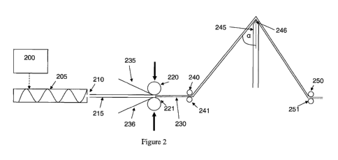
Referring now to Figure 2 which shows a schematic arrangement of the
apparatus used for performing the method, the fluid-bed mixer is illustrated
at
200 and the mixed powders are schematically illustrated as being passed to a
proximal end of the extruder 205. At a distal end of the extruder a narrow die
210 is used to form the initial film 215.
Calendering
In order to reduce the thickness of the film and in order to improve the
surface
smoothness of the opposing surfaces of the film, in many cases it is
preferable
to apply a rolling process, after the extrusion, at step 108. Since this is a
high
pressure rolling treatment involving smooth surfaced rollers, it is a
calendering
treatment in the present case. This is achieved by the use of rollers 220 and
221
upon either side of the initial film 215. These rollers are forced together as
indicated by the arrows 225 using a pressure of between 50 and 200 bar (about
5MPa to 20MPa). It should be noted that the rollers are heated. Even though
the
19
CA 02767241 2012-01-04
WO 2011/004190 PCT/GB2010/051118
material arrives at a temperature not much less than the temperature at which
it
leaves the extruder (around 140 to 150 C), unless the rollers are heated then
contact with them may substantially reduce the surface temperature and cause a
thermal gradient within the film. In the present case a temperature of 120 C
and
200 bar (20MPa) is used for the calendering.
A second function of the rollers 220,221 is to apply an upper cover film 235
to an
upper surface of the initial film 215 and also to apply a corresponding lower
cover film 236 to the lower surface. The cover film in each case is wider than
the
initial film 215 and each cover film 235, 236 is fed between the respective
roller
220, 221 and the surface of the film in question. The cover film in each case
is
formed from polyethylene terephthalate (PET). The heat and pressure applied
by the rollers 220, 221 causes the PET cover films to adhere to the respective
surfaces of the initial film 215. The respective cover films 225, 236 are
shown in
Figure 2 and are applied at step 108 in Figure 1. The calendering by the
rollers
produces a calendered film sandwich at step 110 denoted as a calender film 230
having a width of about 3 cm and a thickness of around 20 micrometres
(excluding the PET cover films).
One additional advantage of the use of the calendering rollers is that the
shape
of the die 210 is not critical and indeed it has been found that a circular
dye may
even be used. Following calendering, the film between the two cover films does
not exhibit much colour.
Although the calendering process is advantageous, particularly for thin films,
it is
not essential for the production of the optical effects according to the
invention.
Since there is however little or only weak colour effects exhibited either by
the
initial film 215 or the calender film 230, a further process for providing
significant
colour enhancement is then needed so as to produce an appreciable optical
effect throughout the film so as to provide the associated benefits for its
intended
applications.
Shearing
In order to produce a strong optical effect, the film is then subjected to a
process
which applies a strong shear force between the opposing (upper and lower)
CA 02767241 2012-01-04
WO 2011/004190 PCT/GB2010/051118
surfaces of the film. Various mechanisms may be used to achieve this although
what is common to each of them is that typically a net force is applied within
one
surface, in the direction of elongation of the film, and substantially
parallel to that
surface, with respect to the opposing surface. This can be thought of as a
force
which will cause the net displacement of one PET cover film with respect to
the
other in a direction of elongation of the film itself.
Returning now to Figure 2, the film sandwich in the form of calendar film 230
is
firstly passed through two tensioning rollers 240, 241 on opposing sides of
the
1o film to ensure that the film is gripped tightly. The film is then passed
over a
heated sharp edge running at least the width of the film. In this case the
edge is
provided as an edge of a metallic heated plate 245. In this case glass fibre
reinforced polytetrafluroethylene (PTFE) is used to coat the edge 246 and
provide a low friction surface. Lines lying parallel with the film elongation
direction and lying within the planes defining the film surface on the
upstream
and downstream sides of the edge make an angle 2a with respect to one
another, this angle being subtended by a plane passing through the edge. As a
result an angle a exists between the upstream film plane and the edge plane
and similarly an angle a exists between the edge plane and the downstream film
plane. On the downstream side of the edge a further pair of tensioning rollers
250 and 251 on opposing sides of the film ensure that the film is kept under
tension and therefore forced against the edge 246.
The application of a tensile stress within the film 230 caused by the rollers
240,
241, 250, 251 causes a retarding force upon the cover film 236 which is
adjacent
the edge in comparison with that of the cover film 235 which is distal from
the
edge. Thus a shear force is applied in the plane of the cover film 236 at the
position of the edge and in a direction of elongation of the film sandwich
230.
The small radius of curvature at the edge 246 forces the proximal and distal
surfaces of the film (with respect to the edge) to experience a different path
length The adhesion between the cover film and the photonic crystal material
to
which it is attached transmits the shear force to the material and causes
local
rearrangement of the polystyrene spheres within it. This enhances the local
crystallinity and thereby increases the ordering which in turn results in an
improved optical effect.
21
CA 02767241 2012-01-04
WO 2011/004190 PCT/GB2010/051118
The resultant optical effect (second optical effect) caused by the shear
process
is, in practice, quite dramatic. In some cases where a visible optical effect
is
produced by the extrusion process, the shear process caused by the edge may
significantly strengthen the effect, causing it to be substantially enhanced.
It will be appreciated that the temperature of the edge 246, together with the
local profile of the edge, the angle 2a and the force applied by the rollers
240,
241, 250, 251 may be altered in accordance with the type of material and its
1o thickness.
Returning to Figure 1, the passage of the film between the nip of the rollers
240,
241 is shown at step 112 where the film is gripped and tension applied.
Thereafter, at step 114 the heating and shearing process is applied by the
edge
246. At step 116 the film is once again gripped by the rollers 250, 251 and at
step 118 additional processing steps may be applied downstream.
It will be recalled that one of the factors in the selection of materials to
use in the
process was a consideration of their ability to cross-link. One such
downstream
process at step 118 may be a cross-linking process such as thermal cross-
linking or cross-linking via application of additional chemicals or radiation
such
as ultraviolet light. In the present example however, the film is cross-linked
due
to the heating process applied by the edge 246 and thereafter over time as it
cools or even remains at ambient temperature for extended periods. Another
such further process is the removal of one or each of the PET films and it
will be
appreciated that certain types of cross-linking may require direct access to
the
surface of the film without the PET cover layer being present.
Although Figure 2 shows the provision of a single heated edge 246 using a
plate
245, it will be appreciated that multiple edges may be used in which
subsequent
edges may be brought into close contact with the same surface or opposing
surfaces, for example in an alternating manner. It is also contemplated that
the
film may be passed two or more times over a single or multiple edges. This may
be achieved by reversing the direction of travel of the film one or more times
(for
example in a "to -and-fro" manner). It will be appreciated that, whilst
relatively
22
CA 02767241 2012-01-04
WO 2011/004190 PCT/GB2010/051118
short "non-continuous" lengths of film may be treated in this way, the same
process can also be applied to continuous films by treating discrete length
sections of the film sequentially which may be effected by the use of guides
or
rollers whose position is moveable thereby changing the local film path
length.
The cover films provide a number of beneficial qualities to the process. They
firstly provide a strengthening effect in that they provide additional support
to the
film as it is thinned by the calender rollers 220, 221. They also provide
protection
for the film as it is passed through the downstream rollers and over the edge
for
example. Another beneficial effect is that the adhesion between the cover film
and the photonic crystal film allows a more even distribution of the shear
stress
thereby providing a homogenous application of the force across the width of
the
film. This assists greatly in providing a homogeneous optical effect.
Whilst the cover films provide these benefits, in some cases the initial film
215
has sufficient strength and mechanical properties to be processed without
either
one or each cover film, if desired. The details of the processing are
essentially
the same as those with the cover film and in this case it will be appreciated
that
the surface properties of the photonic crystal film do not cause adverse
effects
when in contact with the rollers, edge or any other means for producing the
shear process.
A great benefit of the method and apparatus described in connection with
Figures 1 and 2 is that the film can be produced essentially continuously and
also have similar optical properties throughout.
Firstly, Figure 3 shows a more detailed arrangement of the right hand side of
Figure 2, downstream of the rollers 220, 221. The apparatus to the left of
Figure
2 is generally represented in Figure 3 by the left hand apparatus entitled
"feed".
In Figure 3, the surfaces of the various components such as rollers which the
film contacts are described by various letters, these being as follows: steel
(S),
rubber (R), glass or glass fibre fabric (G), heated (H) and cooled (C).
Various
parameters of the components are likewise denoted by letters: torque (M),
force
(F), tension (A), revolutions per minute (V) and temperature (T). The rollers
are
described in the following terms: powered (P), heated (H) and cooled (C).
23
CA 02767241 2012-01-04
WO 2011/004190 PCT/GB2010/051118
With reference to the left hand section marked "transport" 260 the film is
firstly
fed, following leaving the rollers 220, 221 in Figure 2 around two tensioning
rollers which perform the function of rollers 240, 241 in Figure 2. In Figure
3
these rollers are indicated at 261 and the letter M denotes the torque applied
to
the rollers which generates tension within the film. Each of these rollers has
a
rubber surface and is powered. Upon leaving the first transport section 260,
the
film 230 then passes into the colour enhancement unit 265. This includes a
heated chamber 266 into which the film 230 passes. This is then passed around
1o the surfaces of two adjacent rollers indicated at 267 (in a half-figure-of-
eight
path). Each of these rollers is heated (denoted by the letter H) and has a
surface
formed from steel. The steel provides good transfer of the heat to the film.
The
film then passes, whilst remaining in the chamber 266, over a sharpened edge
of the heated plate 270. This is also heated (denoted by H) and in this case
comprises heated glass with a glass fibre fabric edge over which the film 230
is
passed. The film 230 then exits the chamber and passes around the surfaces of
two adjacent rollers 272 (again in a half-figure-of-eight path), these again
being
formed of steel and this time being cooled rollers so as to reduce the
temperature of the film.
The cooled film then passes into a second transport section 280 which, in a
similar manner to the section 260 is equipped with two adjacent rollers 281
about whose surfaces the film is entrained. These rollers again are powered
and
have rubber surfaces so as to grip the film. They apply torque (indicated by
M)
and therefore provide a force indicated by F to the film. The powered rollers
of
the transport sections 260, 280 provide a tensioning force within the film and
ensure that it is driven against the sharp edge provided by the plate 270.
Downstream of the second transport section 280, the film enters the product
section 290 where it is wound around a steel powered roller.
Characterisation of Optical Effect
The spectra of experimental films having PET cover layers and undergoing a
shearing process can be investigated using spectrometry. An example of a
suitable transmissive spectrometer is a Perkin Elmer Lambda 40 spectrometer.
24
CA 02767241 2012-01-04
WO 2011/004190 PCT/GB2010/051118
In the present case this spectrometer was used to characterise the examples.
Two sets of irradiation directions were chosen, one set being in a plane
defined
by axes in the elongate direction of the film and the normal to the film
(denoted
"parallel"), and the other being in a plane parallel to the transverse
direction of
the film and the normal direction to the film (denoted "normal"). In each
case, an
angle ' is defined, this being the angle between the beam within the
respective
plane and the plane of the film itself. This is shown in Figure 4.
The measurements described took into account the individual spectra of the two
PET layers which were first measured separately.
Figures 5a and 5b show respectively the absorption s pectra in the parallel
(Figure 5a) and normal (Figure 5b) arrangements for Sample 1. The spectra
were taken upon a film following a calendering process (such as having
immediately passed through the rollers 220, 221 of Figure 2) and prior to any
colour enhancement step. It will be noted that the absorbent spectra in each
case exhibits some reduction of general gradient around a wavelength of about
500 nanometres, but in each case there is no easily identifiable peak. This
therefore represents the first optical effect. Figures 6a and 6b show the
equivalent spectra for films having passed through the colour enhancement unit
and therefore having been subjected to the shearing process. In each case, a
strong peak is visible between about 500 and 600 nanometres (this representing
the second optical effect). Furthermore, the position of the peak shifts as a
function of the incidence angle (D. This is as predicted by Bragg, the peaks
travel
in the direction of the smaller wavelengths with decreasing angles of (D. This
angular dependency demonstrates that the second optical effect in this case is
an optically variable effect.
Figure 7 shows a comparison between the spectra after the rolling process and
prior to colour enhancement, and after the colour enhancement process.
The spectra demonstrate that a strong angularly dependent colour effect is
provided in each of the normal and parallel illumination directions. Although
not
easily discerned from the Figures 6a and 6b, the form and position of the
peaks
in Figures 6a and 6b demonstrate that a different colour effect is achieved as
a
CA 02767241 2012-01-04
WO 2011/004190 PCT/GB2010/051118
result of illumination at any particular angle in the parallel direction when
compared with the normal direction. Thus, two of the colour effects are not
only
angularly dependent with respect to angle of incidence, they are also
angularly
dependent with respect to rotation angle about the normal of the film.
Similar measurements were also taken in reflection rather than in transmission
and equipment in the form of an Ocean Optics USB4000 spectrometer was used
for this purpose. The films were found to demonstrate a strong reflective
colour
effect and, despite the transparency of the films, the colour of any substrate
beneath the films was found to have only limited effects upon the strong Bragg
colours provided by the film, as is demonstrated in Figures 8a and 8b which
relate to the position of the Bragg peak with a film having a black support
(Figure
8a) and a white support (Figure 8b). Thus can be seen, an angle of incidence
shifting from 45 degrees to 75 degrees causes a shift in the Bragg peak by 65
nanometres. This in practice causes a colour change from orange-red at the 75
degrees position to a bluish-green at 45 degrees. It should be noted that the
angles described are measured between the light source and the film plane. The
detector is therefore placed in the symmetrical position at the angle 180
degrees
minus 0. The symmetrical arrangement did therefore include a contribution from
the surface gloss. Measurement at off-gloss angles shows that the film
actually
reflects the colour into an angle cone surrounding the gloss angle. Figure 9
illustrates the effect of off-gloss angles and even at an angle of about 70
degrees off the gloss angle, a notable peak can still be seen in Figure 9.
As has been demonstrated, the film production method of the present invention
provides a strong photonic optical effect in photonic material films by the
application of a shear process. This has numerous potential applications,
including incorporation as a security device to reduce counterfeiting, since
similar optical effects are extremely difficult to replicate by known
processes.
Some examples of the incorporation of photonic crystal material films into
security devices and documents are now discussed. Each of the examples now
described refers to two regions of photonic crystal material, these being
denoted
Region A and Region B. In each example the intention is to describe two
different alternative situations. The first is that Region A and Region B are
26
CA 02767241 2012-01-04
WO 2011/004190 PCT/GB2010/051118
identical and therefore interchangeable such that the material in each of
Regions
A and B is formed from the photonic material film discussed earlier. The
second
alternative is that Regions A or B have different properties. This might be
because, during the extrusion process, the component materials and/or the
processing are modified as a function of time, and/or across the dimension of
the film. As a further alternative, or addition, a further process may be
applied to
part of the film (such as a localised thermal and/or mechanical process) to
modify the material properties. Regions A and B may also be distinct because
they represent cut-out parts of different films, applied separately.
Figure 10 shows a security device formed using a film of the current invention
incorporated into a security document, as a surface applied patch. Figure 11
shows
a cross-sectional view of the patch on the document in Figure 10. The device
comprises parts of self-supporting photonic crystal films in the form of two
Regions
A and B, onto which is applied a dark absorbing layer. An adhesive layer is
applied
to the outer surface of the device on the dark absorbing layer to adhere it to
the
secure document. Regions A and B exhibit different optically variable effects,
since
each region was produced using material from a different film. Region A has an
angular dependent colour variation in response to incident light. For example
the
angular dependent colourshift in Region A can be from red, when viewed at a
relatively high angle of incidence, for example 70 , to the plane of
substrate, to
green when viewed at a more oblique angle of incidence, for example 45 , to
the
plane of the substrate. In contrast the angular dependent colourshift in
Region B can
be from green, when viewed at 70 to the plane of substrate, to blue when
viewed at
45 of incidence to the plane of the substrate.
One or both of the regions A and B are preferably in the form of a design. In
the
case of complex designs, one of the regions may be formed by a deformation
process (such as stamping) in which case the relevant region may not be
optically
variable. Preferably the designs are in the form of images such as patterns,
symbols
and alphanumeric characters and combinations thereof. The designs can be
defined
by patterns comprising solid or discontinuous regions which may include for
example line patterns, fine filigree line patterns, dot structures and
geometric
patterns. Possible characters include those from non-Roman scripts of which
examples include but are not limited to, Chinese, Japanese, Sanskrit and
Arabic.
27
CA 02767241 2012-01-04
WO 2011/004190 PCT/GB2010/051118
Figure 12 shows an example security device using a film of the current
invention
incorporated into a security document as a windowed thread with windows of
exposed thread and areas of embedded thread. The thread comprises longitudinal
bands, corresponding to Regions A and B, which exhibit different angular
dependent
colour variations. The bands are formed in the photonic crystal film by
varying the
sphere size of the polymer system during the extrusion process. Figure 13
shows a
cross-sectional view of one example of the current invention suitable for
application
as a windowed security thread. The device comprises a self-supporting photonic
crystal film, comprising regions A and B, onto which is applied a dark
absorbing
layer. An adhesive layer may be applied to the outer surfaces of the device to
improve adherence to the secure document.
In an alternative structure to that shown in Figure 13, and illustrated in
Figure 14, the
security device comprises a polymeric carrier substrate, for example
Polyethylene
Terephthalate (PET) or Bi-axially Oriented Polypropylene (BOPP), onto which is
applied a dark absorbing layer. A layer of photonic crystal material,
comprising
contrasting optically variable Regions A and B, is then applied to the
opposite
surface of the carrier film, or alternatively on to the dark absorbing layer.
The
photonic crystal layer is formed as a separate film and then laminated to the
carrier
substrate. This is particularly beneficial when the carrier substrate for the
security
thread comprises additional security features, such as magnetic layers and
metallised layers comprising demetallised characters, which may not be
suitable to
be applied directly to the photonic crystal layer. An adhesive layer may be
applied to
the outer surfaces of the device to improve adherence to the secure document.
The fact that the security device in Figures 12, 13 and 14 is in the form of a
windowed security thread is for illustration only and the photonic crystal
material
could just as easily be employed as part of a surface applied security feature
such
as a stripe or a patch.
The examples described in Figures 12 to 14 are viewed primarily in reflection
and as
such the optical effects of the photonic crystal material are best visualised
against a
dark non-selectively absorbing background. This can be achieved by placing an
absorbing layer under the photonic crystal layer or by the introduction of
absorbing
particles into the photonic crystal materials.
28
CA 02767241 2012-01-04
WO 2011/004190 PCT/GB2010/051118
Whilst the use of a black, or very dark, substantially totally absorbing layer
may give
rise to the most strong colourshifts, other effects may be generated by the
use of a
partially absorbing layer of other colours or a combination of colours, giving
rise to
differing apparent colourshift colours. The absorbing layer may comprise a
pigmented ink or coating or alternatively a non-pigmented absorbing dye can be
used.
Security devices comprising photonic crystal materials are inherently machine-
readable due to the wavelength selectivity of the photonic crystal materials.
In
further examples the machine readable-aspect of the current invention can be
extended further by the introduction of detectable materials in the photonic
crystal or
by the introduction of separate machine-readable layers. Detectable materials
that
react to an external stimulus include but are not limited to fluorescent,
phosphorescent, infrared absorbing, thermochromic, photochromic, magnetic,
electrochromic, conductive and piezochromic materials.
In one preferred embodiment, the pigment in the separate absorbing layers is
machine-readable, for example carbon black, to produce a machine-readable,
conducting or IR absorbing layer. Alternatively it may be a magnetic material,
such
as magnetite, to produce a machine-readable magnetic layer.
The security device incorporating the film of the current invention could be
used in
combination with existing approaches for the manufacture of security thread.
Examples of suitable methods and constructions that can be used include, but
are
not limited to, those cited within W003061980, EP0516790, W09825236, and
W09928852.
Figure 15a illustrates how the current invention can be combined with
demetallised
characters for application as a windowed security thread. The method requires
a
metallised film comprising a substantially clear polymeric film of PET or the
like,
which has an opaque layer of metal on a first side thereof. A suitable pre-
metallised
film is metallised MELINEX S film from DuPont of preferably 19 m thickness.
The
metal layer is printed with a resist which contains a black or dark dye or
pigment.
Suitable resists include the dye BASF Neozapon X51 or the pigment (well
29
CA 02767241 2012-01-04
WO 2011/004190 PCT/GB2010/051118
dispersed) "Carbon Black 7" mixed into a material with both good adhesion to
metal
and caustic resistance.
The printed metallised film is then partially demetallised, according to a
known
demetallisation process using a caustic wash which removes the metal in the
regions not printed with the resist. The remaining regions coated with resist
provide
a black layer which is visible when the demetallised film is viewed from its
first side
(along arrow Y) interspersed with clear regions. The shiny metal of the
remaining
parts of the metallic layer are only visible from an opposite side of the
demetallised
film (along arrow X). The resist may be printed in the form of the indicia
such as
words, numerals, patterns and the like; in which case the resulting indicia
will be
positively metallised, with the metal still covered by the dark or black
resist.
Alternatively the resist may be printed so as to form indicia negatively, in
which case
the resulting indicia will be provided by the demetallised regions. The
indicia
however formed, are clearly visible from both sides, especially in transmitted
light,
due to the contrast between the regions of the metal which have been removed
and
the remaining opaque regions. The photonic crystal film is then applied.
The security device illustrated in Figure 15a exhibits two visually
contrasting security
characteristics. The device comprises the optical effects of the photonic
crystal
layer, as described for the previous examples, when the finished substrate is
viewed
in reflection from the first side (along arrow Y); and a metallic shiny
partial coating
when viewed from the other side (along arrow X). Additionally clear positive
or
negative indicia, defined by the black resist, can be seen in transmission
from either
side. This example is particularly advantageous when used in a device that is
viewable from both sides of the document in which it is incorporated. For
example
the device could be incorporated into a secure document using the methods
described in EP1141480 or W003054297.
Figure 15b illustrates a machine-readable version of the device illustrated in
Figure
15a. The device comprises a metallised PET base layer demetallised with a
suitable
design including tramlines of metal left along each edge of the device. As
described
with reference to Figure 15a a black resist is used during the demetallisation
process. A protective layer may be applied onto the metal tramlines (not shown
in
Figure 15b) to prevent the metal from being corroded by the magnetic layer,
which is
applied next. A suitable protective layer is VHL31534 supplied by Sun Chemical
CA 02767241 2012-01-04
WO 2011/004190 PCT/GB2010/051118
applied with coat weight of 2gsm. The protective layer may optionally be
pigmented.
The magnetic material is only applied over the metal tramlines so as not to
obscure
the demetallised indicia. The photonic crystal film layer is then applied. An
adhesive
layer may be applied to the outer surfaces of the device to improve adherence
to the
security document.
When a magnetic material is incorporated into the device either within the
absorbing
layer or as a separate layer the magnetic material can be applied in any
design but
common examples include the use of magnetic tramlines or the use of magnetic
blocks to form a coded structure. Suitable magnetic materials include iron
oxide
pigments (Fe2O3 or Fe304), barium or strontium ferrites, iron, nickel, cobalt
and
alloys of these. In this context the term "alloy" includes materials such as
Nickel:Cobalt, Iron:Aluminium:Nickel: Cobalt and the like. Flake Nickel
materials can
be used; in addition Iron flake materials are suitable. Typical nickel flakes
have
lateral dimensions in the range 5-50 microns and a thickness less than 2
microns.
Typical iron flakes have lateral dimensions in the range 10-30 microns and a
thickness less than 2 microns.
In an alternative machine-readable embodiment a transparent magnetic layer can
be incorporated at any position within the device structure. Suitable
transparent
magnetic layers containing a distribution of particles of a magnetic material
of a size
and distributed in a concentration at which the magnetic layer remains
transparent
are described in W003091953 and W003091952.
In a further example the security device of the current invention may be
incorporated
in a security document such that the device is incorporated in a transparent
region
of the document. The security document may have a substrate formed from any
conventional material including paper and polymer. Techniques are known in the
art
for forming transparent regions in each of these types of substrate. For
example,
W08300659 describes a polymer banknote formed from a transparent substrate
comprising an opacifying coating on both sides of the substrate. The
opacifying
coating is omitted in localised regions on both sides of the substrate to form
a
transparent region.
31
CA 02767241 2012-01-04
WO 2011/004190 PCT/GB2010/051118
EP1141480 describes a method of making a transparent region in a paper
substrate. Other methods for forming transparent regions in paper substrates
are
described in EP0723501, EP0724519, EP1398174 and WO03054297.
Figure 16 shows the film of the current invention incorporated into a
transparent
region of a security document. Figure 17a shows a cross-sectional view of the
security device within the transparent region. The security device comprises a
transparent carrier layer, which preferably forms the transparent region of
the
substrate. An absorbing material is applied to the transparent layer in
localised
regions to form a recognisable pattern or identifying image. A layer
comprising a film
of photonic crystal material, comprising two Regions A and B, exhibiting the
same
optical characteristics as the Regions A and B in Figures 12 and 13, is
located
above the absorbing layer.
When the device in Figure 18 is viewed in reflection from side A, two
different highly
contrasting colourshifting regions are observed in Regions A and B, from the
areas
of the photonic crystal layer located above the absorbing layer, as the device
is
tilted. For example in Region A the colourshift can be from red, when viewed
at one
angle of incidence to the plane of substrate, to green when viewed at a more
oblique
angle of incidence to the plane of the substrate. In Region B a different
colourshift
will apply, over the same angular range, for example green to blue. In the
regions
not above the absorbing layer the transmitted colour saturates the reflective
colour.
The transmitted and reflected colours are complementary, for example, a red to
green colourshift in reflection is seen as a cyan to magenta colourshift in
transmission.
When the device in Figure 17a is viewed in reflection or transmission from
side B
the dark absorbing layer will be visible in the form of an identifying image.
If a dark
image is not aesthetically acceptable then a more aesthetically pleasing
material/colour could be used to conceal the dark layer such that it is not
viewable
from side B. For example the dark absorbing areas could be overprinted on side
B
of the transparent region with differently coloured opaque inks or metallic
inks.
Alternatively the transparent carrier substrate could be replaced with a
metallised
polymeric substrate, as illustrated in Figure 17b. The metallised substrate is
printed
with a dark resist, as discussed with reference to Figure 15a, in the form of
the
identifying image. The printed metallised film is then partially demetallised
removing
32
CA 02767241 2012-01-04
WO 2011/004190 PCT/GB2010/051118
the metal in the regions not printed with the resist. When viewing from side A
the
photonic crystal film is viewed against the absorbing dark resist and appears
as
described with reference to Figure 17a, but when viewing from side B a
metallic
image is observed of the identifying image printed with the dark resist. The
image
could be positive, i.e. defined by the metallic regions, or negative, i.e.
defined by the
transparent regions between the metallic regions. As mentioned earlier, each
of
Region A and Region B may be identical and formed from continuous film or cut-
out
sections thereof, rather than exhibiting different optical effects.
In an alternative machine-readable construction the dark resist in Figure 17b
can be
formed using a magnetic pigment, for example magnetite to provide a machine-
readable code. In a further embodiment, only part of the dark resist is
provided with
a magnetic pigment and the remainder is provided with a non-magnetic pigment.
If
both the magnetic and non-magnetic regions are substantially totally absorbing
there will be no visual difference in the photonic crystal film over the two
regions and
therefore the format of the code will not be readily apparent.
Figure 18 illustrates an example where the film of the current invention is
incorporated into an aperture of a paper substrate. A self-supporting photonic
crystal
film is incorporated into a paper substrate as described in EP1141480. One
side of
the photonic crystal film is wholly exposed on the front surface of a paper
substrate
in which it is partially embedded (Figures 18a and 18c), and partially exposed
in one
aperture on the rear surface of the substrate (Figures 18b and 18d). In this
example
carbon nanoparticles have been incorporated into the photonic crystal
structure.
The photonic crystal film comprises two regions A and B. Region A appears red
when viewed at one angle of incidence to the plane of the substrate and shifts
to
green when viewed at a more oblique angle of incidence to the plane of the
substrate. Region B is a non-opalescent region due to an area of disorder in
the
photonic crystal structure (for example caused by deforming a region of the
film
following its formation) and its appearance remains constant at any viewing
angle. In
this example Region A forms the background and Region B forms the identifying
image "DLR".
On viewing the device at one angle of incidence to the plane of substrate, for
example 70 , Region A appears red and the non-opalescent identifying image
"DLR"
33
CA 02767241 2012-01-04
WO 2011/004190 PCT/GB2010/051118
is visible against the red background (Figures 18a and 18b). On tilting to a
more
oblique angle of incidence, for e.g. 45 , the colour of Region A shifts from
red to
green but the appearance of Region B remains the same and therefore the
identifying image "DLR" is visible against the green background (Figures 18c
and
18d). This effect is visible from both sides of the security document.
The use of the self-supporting photonic crystal film doped with carbon
nanoparticles
enables the reflective colourshifting effect to be visible from both sides of
the
document while using just a single layer of colourshifting material. On
viewing the
device from the rear of the document in reflection, illustrated in Figure 18b,
the same
optical properties in Regions A and B, as is observed from the front of the
document, is present where the photonic crystal film is exposed in the
aperture.
In an alternative embodiment to that referenced in Figure 18 the photonic
crystal film
can be supported by a carrier layer to facilitate its incorporation into the
paper
document. The photonic crystal layer is formed as a separate film (including
the
application of shearing) and then laminated to the carrier substrate. The
carrier
substrate may comprise additional security features including de-metallised
designs,
holographic designs in combination with a highly reflective layer such as a
metallic
layer or a thin transparent layer of a high refractive index material (for
example
ZnS), printed indicia, luminescent or magnetic materials, and coarse embossing
with
a security design that may be either blind embossed to produce a
tactile/visible
feature or could include printing inks to further enhance visibility. In this
manner a
different security feature can be observed on either side of the security
device.
In a further embodiment a security device can be constructed such that
different
colourshifting effects are observed on either surface of the security device.
This can
be achieved by laminating together two photonic crystal films with different
optical
characteristics or by varying the optical characteristics of the photonic
crystal film
over the thickness of the film.
Different colourshifting effects on either surface of the security device can
also be
generated using a single layer of photonic crystal film by locally varying the
optical
characteristics of the photonic crystal film over the thickness of the film.
For example
the sphere size can be varied through the thickness of the film. This
variation can be
34
CA 02767241 2012-01-04
WO 2011/004190 PCT/GB2010/051118
introduced by controlling the assembly of the spheres during the formation of
the
photonic crystal film. Alternatively if the film is manufactured by polymer
extrusion
then two polymer mixes, comprising the spheres and the matrix, can be
generated
with different sphere sizes. The two polymer mixes can then be co-extruded
into a
single polymer film forming a crystal structure where there is a step change
in
sphere size at an interface in the centre of the film.
Regions with different optical characteristics across the film are
particularly useful
for inclusion in thicker security devices (>100 m) which might be employed as
layers in card based documents such as a credit cards, debit cards, identity
cards
and driving licences.
The security devices described may be further customised in order to increase
the
difficulty in counterfeiting and/or provide identifying information. The
customisation
process can take place before or after the device is incorporated into the
document.
In one example the customisation of the security device occurs by applying
printed
information to the photonic crystal film. The photonic crystal film may be
printed with
images using any of the conventional printing processes such as intaglio,
gravure,
ink jet, offset lithography, screen, dye diffusion and flexography. The print
may be
applied as a single print working in a single colour or as multiple print
workings in
multiple colours.
In a preferred embodiment the images are printed partly on the photonic
crystal film
and partly on the substrate the device is incorporated into, such that the
design
continues uninterrupted between the two surfaces. In a further embodiment, one
of
the colours of the printed images matches one of the switching colours of the
photonic crystal film. For example if one of the regions of the photonic
crystal film
switches from red to green on tilting the device in a specific viewing
direction then
any red printed information over this region will be substantially invisible
at certain
angles of incidence but becomes visible as the sample is tilted and the static
red of
the printed information contrasts with the green of the optically variable
photonic
crystal film. In this manner a latent image security feature can be created.
As an alternative to the printing of ordinary coloured inks, it is also
possible to print
functional inks. By functional inks we mean inks that react to an external
stimulus.
Inks of this type include but are not limited to fluorescent, phosphorescent,
infrared
CA 02767241 2012-01-04
WO 2011/004190 PCT/GB2010/051118
absorbing, thermochromic, photochromic, magnetic, electrochromic, conductive
and
piezochromic.
As well as functional inks, it is also possible to print onto the photonic
crystal film
with other optical effect inks. Optical effect inks include OVI and Oasis
marketed
by Sicpa. Other optical inks include inks containing iridescent, iriodine,
pearlescent,
liquid crystal and metal-based pigments.
In a further embodiment non-opalescent regions are created by mechanically
deforming the photonic crystal film. The mechanical deformation is preferably
carried out using an embossing or hot stamping process. Preferably the
embossing
process takes place during the intaglio printing process and is carried out
using an
intaglio plate. Figure 19 shows an example of a security substrate comprising
a
security device where the photonic crystal film has been customised by hot
stamping the film after it has been applied to the base substrate. In this
example the
photonic crystal film has been incorporated into a paper substrate in the same
manner as referenced in Figure 18 and described in EP1141480. Figure 19 shows
the front surface of the paper substrate on which the device is wholly
exposed. The
device is also exposed on the back surface in the aperture region. In this
example
the photonic crystal film exhibits a red-green colourshift on tilting the
device to an
oblique angle of incidence. An image of the numeral "5" is hot stamped into
the
photonic crystal film such that the order of the photonic crystal is distorted
in the
stamped region. The disorder in the crystal results in the stamped regions
becoming
non-opalescent at all angles of view. On tilting the document the numeral "5"
remains non-opaslescent but the non-stamped regions change from red (Figure
19a) to green (Figure 19b).
In a further embodiment, the customisation of the security device occurs by
embossing the photonic crystal film with raised line structures. The embossing
of
raised line structures into photonic crystal films is particularly
advantageous
because the facets generated by the embossing result in a change in the angle
of
incidence of the incoming light, generating facets of differing colours due to
the fact
that the colour of the photonic crystal film is dependent on the angle of
view. The
use of a raised line structure with an photonic crystal film has two secure
aspects;
firstly the optically variable feature generated by the line structure and
secondly the
36
CA 02767241 2012-01-04
WO 2011/004190 PCT/GB2010/051118
creation of localised regions exhibiting different colourshifts from the
background
film.
For example if the photonic crystal device exhibits a green to blue
colourshift on
tilting the device away from normal incidence then when viewed at normal
incidence
the embossed and non-embossed regions will appear green. On tilting the device
the non-embossed and embossed regions will change from green to blue at
different
angles of view as the device is tilted.
A further advantage of using embossed raised line structures is that the
structures
have a raised surface that can be identified by touch. The smooth surface of
the
photonic crystal film further enhances the tactility of these raised
structures.
The embossed line structures can take any convenient form including straight
(rectilinear) or curved such as full or partial arcs of a circle or sections
of a
sinusoidal wave. The lines may be continuous or discontinuous and, for
example,
formed of dashes, dots or other shapes. By other shapes we mean the dots or
dashes could have a graphical form. The line widths are typically in the range
10-
500 microns, preferably 50-300 microns. Preferably, the individual lines are
barely
visible to the naked eye, the main visual impression being given by an array
of
multiple lines. The lines can define any shape or form, for example square,
triangle,
hexagon, star, flower or indicia such as a letter or number.
The embossed line structures are preferably formed by applying an embossing
plate
to the photonic crystal film under heat and pressure. Preferably the embossing
process takes place during the intaglio printing process and is carried out
using an
intaglio plate having recesses defining the line structures. Preferably the
photonic
crystal film is blind embossed, i.e. the recesses are not filled with ink.
However it is
also possible that some of the recesses defining the embossed structure may be
filled with ink and others left unfilled. Further intaglio printing or blind
embossing may
be carried out on regions of the substrate adjacent to the security device
using the
same intaglio plate so as to achieve precise registration between the
different
regions.
Figure 20 shows an example of a security substrate comprising a security
device
where the photonic crystal film has been customised by embossing the film
after it
has been applied to the base substrate. In this example the photonic crystal
film has
37
CA 02767241 2012-01-04
WO 2011/004190 PCT/GB2010/051118
been incorporated into a paper substrate in the same manner as referenced in
Figure 18 and described in EP1141480. Figure 20 shows the front surface of the
paper substrate on which the device is wholly exposed. The device is also
exposed
on the back surface in the aperture region. In this example the photonic
crystal film
exhibits a red-green colourshift on tilting the device to an oblique angle of
incidence
and viewing along viewing direction 1 and a green-blue colourshift on tilting
the
device to an oblique angle of incidence and viewing along viewing direction 2.
The
embossed line structures, formed by a respective set of substantially parallel
raised
lines, define the numeral "5".
On viewing the substrate along viewing direction 1 at a relatively high angle
of
incidence, for example 70 to the plane of the substrate the non-embossed
regions
appear red but the embossed regions appear green due to the dominant reflected
light arising from the edges of the raised lines. The difference in colour
arises
because the effective angle of incidence for light incident on the edge
regions is
greater than the angle of incidence for light incident on flat non-embossed
regions.
On tilting the substrate to a more oblique angle of incidence the non-embossed
regions switch from red to green and the embossed regions switch from green to
blue. If the device is rotated by 90 , such that it is viewed along viewing
direction 2
the embossed and non-embossed regions appear substantially the same colour at
a
given viewing angle because very little light is reflected by the edge of the
lines.
In a further embodiment the customisation of the security device occurs by
embossing the photonic crystal film with a non-diffractive line structure. A
non-
diffractive line structure is an example of a raised line structure which
produces an
optically variable effect when the angle of incidence light varies, but in
which this
effect is not caused by interference or diffraction. Security devices based on
non-
diffractive line structures are known in the prior art for example W09002658
describes a security device in which one or more transitory images are
embossed
into a reflective surface. W09870382 discloses a further security device in
which a
group of elemental areas in which lines extend at different angles from each
other
form respective image pixels. US1996539 discloses a decorative device in which
a
relief structure is formed in a surface and has an optically variable effect.
W02005080089 discloses a security device which has segments defined by line
structures in a reflective portion of a substrate, which cause incident light
to be
reflected non-diffractively as the angle of incidence changes.
38
CA 02767241 2012-01-04
WO 2011/004190 PCT/GB2010/051118
In an alternative embodiment the security device further comprises an
optically
variable device such as a hologram or diffraction grating. These devices are
commonly formed as relief structures in a substrate, which is then provided
with a
reflective coating to enhance the replay of the device. In the current
invention the
photonic crystal can act as the reflective coating and the relief structure
can be
embossed directly into the photonic crystal film or into an embossing lacquer
applied
onto the photonic crystal film. Alternatively localised regions of the device
can be
provided with a metallised layer and the relief structure subsequently
embossed into
an embossing lacquer on top of the metallised layer. In this manner the device
comprises two laterally spaced regions one exhibiting the colourshifting
properties of
the photonic crystal film and one exhibiting the optically variable properties
of a
holographic device. Alternatively the metallic reflective coating can be
replaced with
a transparent reflection enhancing materials for example a thin layer of a
high
refractive index material such as ZnS. In this case both the colourshifting
properties
of the photonic crystal material and the optically variable properties of the
holographic device are visible in all areas of the device although the
optically
variable properties of the holographic device will only be visible at certain
angles of
view.
In a further embodiment of the invention the security device can be customised
by
the application of a scattering layer to the photonic crystal film. In a
preferred
embodiment the scattering layer takes the form of a matt varnish or lacquer.
In this
context a matt varnish or lacquer is one that reduces the gloss of the
photonic
crystal film by scattering the light reflected from it. One example of a
suitable matt
varnish is a suspension of fine particles in an organic resin. The surface
particles
scatter the light as it passes through the varnish resulting in a matt
appearance. A
suitable varnish for the present invention is "Hi-Seal 0 340" supplied by Hi-
Tech
Coatings Ltd. In an alternative solution the fine particles can be replaced by
organic
waxes. As a further alternative, the scattering layer can be generated by
embossing
a matt structure into the surface of a photonic crystal layer. Suitable
embossed matt
structures are described in W09719821. The scattering layer modifies the
colourshifting properties of the photonic crystal layer.
The scattering layer modifies the surface of the photonic crystal film such
that the
reflection is now more diffuse reducing the glare of the photonic crystal film
and
changing the angular range over which the respective colours of the security
device
are easily viewable to the authenticator. For example, if the photonic crystal
material
39
CA 02767241 2012-01-04
WO 2011/004190 PCT/GB2010/051118
exhibits a red to green colourshift on tilting the device away from normal
incidence
then the switch from red to green occurs closer to normal incidence for the
region
with the scattering layer compared to one without a scattering layer.
Figure 21 illustrates a further example where there are gaps present in the
photonic
crystal film. The device in Figure 21 comprises a photonic crystal film which
has
been transferred onto a substantially transparent carrier substrate.
Alternatively a
self-supporting photonic crystal film can be used without the need for a
carrier
substrate. The photonic crystal film is the same as that described in relation
to
Figure 18 and carbon nanoparticles have been incorporated into the photonic
crystal
structure to produce a substantially opaque film with an intense red colour
when
viewed at normal incidence. A laser is used to form gaps in the photonic
crystal film
in the form of an identifying image. The identifying image is clearly visible
from both
sides, especially in transmitted light due to the contrast between the regions
of the
substantially opaque photonic crystal film which have been removed and the
remaining opaque regions. The security device illustrated in Figure 21
exhibits two
visually contrasting security characteristics; firstly the optical effects of
the photonic
crystal film and secondly the identifying image clearly visible in
transmission from
either side of the device.
In yet a further embodiment of the present invention, photonic crystal
materials can
be selected such that at certain angles of view for at least one of the
Regions A and
B the reflected light is in the non-visible wavelengths of the electromagnetic
spectrum.
In all of the examples the designs or identifying images created by any of the
layers,
for example the photonic crystal film, the absorbing or customising layers,
can take
any form. Preferably the designs are in the form of images such as patterns,
symbols and alphanumeric characters and combinations thereof. The designs can
be defined by patterns comprising solid or discontinuous regions which may
include
for example line patterns, fine filigree line patterns, dot structures and
geometric
patterns. Possible characters include those from non-Roman scripts of which
examples include but are not limited to, Chinese, Japanese, Sanskrit and
Arabic.
It will further be appreciated that in each of the examples described above
one of
the Regions A and B may exhibit an optically variable effect whereas the other
CA 02767241 2012-01-04
WO 2011/004190 PCT/GB2010/051118
region may either exhibit an optical effect in the form of an optically
variable effect or
a non-optically varying effect.
We now describe some examples of methods of forming an optically variable
security device.
Referring to the flow diagram of Figure 22, at step 118 a photonic crystal
film,
processed in accordance with Figure 1 is provided.
At step 120, the film is passed into a hot stamping apparatus which performs a
hot
stamping process upon the material, causing localised deformation. The hot
stamping apparatus applies pressure to selected areas of the film, these areas
comprising, for example, regions corresponding to Region B in the earlier
examples.
In this case the process is performed at an elevated temperature which is in
excess
of the glass transition temperature of the polystyrene. The temperature may
even be
in excess of the melting temperature of the polystyrene. A heated die, stamp
or
roller can be used to perform this function. The hot stamping process causes
the
opal-like structure of the film to be disrupted by permanently plastically
deforming or
melting the spheres, causing them to amalgamate and lose their relative
ordered
structure. It should be noted that a heated stamp, die or roller may be used
having a
geometry such that the parts of the material corresponding to Region B are
formed
according to particular indicia or indeed negative indicia (whereby indicia
themselves are formed from the boundaries of the second region).
The film is then optionally cooled and, in step 122, an adhesive layer may be
applied.
Following the application of adhesive, at step 124 the photonic crystal film
is then
adhered to a substrate material such as a banknote, credit card, passport or
other
document of value. At step 126 various finishing processes are performed such
as
further printing, laminating, cutting and processes for adding further
security
features.
Thus a security document is produced having a photonic crystal material with
regions exhibiting an optically variable effect, and other regions in which a
different
41
CA 02767241 2012-01-04
WO 2011/004190 PCT/GB2010/051118
optical effect is observed, which in the present case is not optically
variable. In the
present case, these latter regions may therefore appear to have a diffuse
translucent appearance which contrasts with the optically variable appearance
of the
other regions. One of the key advantages of this is that each of these regions
is
contained within the same continuous film which is more difficult to
counterfeit.
One particular alternative to the hot stamping process discussed in
association with
step 120 is the use of a modified process in which the temperature of the hot
stamp/die/roller is such that the material is heated to a temperature between
the
glass transition temperature of the matrix and that of the spheres themselves.
This
allows the spheres to remain substantially solid and yet able to move within
the
material matrix. Using an appropriately shaped stamp for example, such as one
having a very shallow inclined surface, the spheres may be caused to partition
away
from parts of the material so as to form a region of only PEA matrix with
substantially no spheres present. In this case the spheres are not destroyed
but are
rather displaced to an area around the region in question. Thus, the
substantially
sphere-free region and the region into which the spheres are displaced may
exhibit
individual and different optical effects, again providing enhanced security
against
counterfeiting.
In the examples described herein, involving the use of deformation processes
such
as stamping and rolling where the film is deformed between two members, then
it
will be appreciated that these members may have a symmetrical form and apply
equal deformation upon each side of the film. In other cases a first one of
the
members may be fixed in position with the other being arranged to moved
towards
the first, with the film therebetween.
Whilst the above example in association with Figure 22 has been discussed with
the
use of an adhesive so as to bond the device to a document of value, it will be
appreciated that a film produced according to these processes could be
incorporated into a document of value such as a banknote by a process similar
to
the formation of a windowed thread using watermarking techniques.
42