Note: Descriptions are shown in the official language in which they were submitted.
CA 02767522 2012-01-06
WO 2011/005964 PCT/US2010/041374
1
HYBRID CONDUCTORS AND METHOD OF MAKING SAME
TECHNICAL FIELD
[0001] The present invention relates to electrical and thermal conductors, and
more
particularly, to hybrid conductors having enhanced conductivity and current
capacity
over a wide range of frequencies.
BACKGROUND ART
[0002] Carbon nanotubes are known to have extraordinary tensile strength,
including
high strain to failure and relatively high tensile modulus. Carbon nanotubes
may also
be highly resistant to fatigue, radiation damage, and heat. To this end, the
addition of
carbon nanotubes to composite materials can increase tensile strength and
stiffness of
the composite materials.
[0003] Within the last fifteen (15) years, as the properties of carbon
nanotubes have
been better understood, interests in carbon nanotubes have greatly increased
within
and outside of the research community. One key to making use of these
properties is
the synthesis of nanotubes in sufficient quantities for them to be broadly
deployed.
For example, large quantities of carbon nanotubes may be needed if they are to
be
used as high strength components of composites in macroscale structures (e.g.,
structures having dimensions greater than 1 cm).
[0004] One common route to nanotube synthesis can be through the use of gas
phase
pyrolysis, such as that employed in connection with chemical vapor deposition.
In
this process, a nanotube may be formed from the surface of a catalytic
nanoparticle.
Specifically, the catalytic nanoparticle may be exposed to a gas mixture
containing
carbon compounds serving as feedstock for the generation of a nanotube from
the
surface of the nanoparticle.
[0005] Recently, one promising route to high-volume nanotube production has
been
to employ a chemical vapor deposition system that grows nanotubes from
catalyst
particles that "float" in the reaction gas. Such a system typically runs a
mixture of
reaction gases through a heated chamber within which the nanotubes may be
generated from nanoparticles that have precipitated from the reaction gas.
Numerous
CA 02767522 2012-01-06
WO 2011/005964 PCT/US2010/041374
2
other variations may be possible, including ones where the catalyst particles
may be
pre-supplied.
[0006] In cases where large volumes of carbon nanotubes may be generated,
however, the nanotubes may attach to the walls of a reaction chamber,
resulting in the
blockage of nanomaterials from exiting the chamber. Furthermore, these
blockages
may induce a pressure buildup in the reaction chamber, which can result in the
modification of the overall reaction kinetics. A modification of the kinetics
can lead
to a reduction in the uniformity of the material produced.
[0007] An additional concern with nanomaterials may be that they need to be
handled
and processed without generating large quantities of airborne particulates,
since the
hazards associated with nanoscale materials are not yet well understood.
[0008] The processing of nanotubes or nanoscale materials for macroscale
applications has steadily increased in recent years. The use of nanoscale
materials in
textile fibers and related materials has also been increasing. In the textile
art, fibers
that are of fixed length and that have been processed in a large mass may be
referred
to as staple fibers. Technology for handling staple fibers, such as flax,
wool, and
cotton has long been established. To make use of staple fibers in fabrics or
other
structural elements, the staple fibers may first be formed into bulk
structures such as
yarns, tows, or sheets, which then can be processed into the appropriate
materials.
[0009] Accordingly, it would be desirable to provide a material that can take
advantage of the characteristics and properties of carbon nanotubes, so that a
conductor made of carbon nanotubes can be processed for end use applications.
SUMMARY OF THE INVENTION
[0010] The present invention provides, in accordance with one embodiment, a
hybrid
conductor comprising a plurality of nanostructures, each having a surface
area; a
member having a geometric profile defined by the plurality of nanostructures;
and a
conductive material positioned so that it is in contact with less than the
total surface
area of the plurality of nanostructures, wherein the combination of the
conductive
material and the plurality of nanostructures enhances conductivity while
decreasing
resistivity along the length of the member.
CA 02767522 2012-01-06
WO 2011/005964 PCT/US2010/041374
3
[0011] In one embodiment, the nanostructures are made from one of carbon,
copper,
silver, boron, boron-nitride, or a combination thereof. In one embodiment, the
plurality of nanostructures are doped in a solution having one of fluoride
salt, chloride
salt, bromide salt, iodate salt, nitrate salt, sulfate salt, or a combination
thereof. In one
embodiment, the member defined by the pluarlity of nanostructures includes one
of a
yarn or a sheet. In one embodiment, the member includes one of a plurality of
yarns,
a plurality of sheets, or a combination thereof. In one embodiment, the
conductive
material includes one of a conductive coating in contact with less than the
total
surface area of the plurality of nanostructures, a conductive wire in contact
with less
than the total surface area of the plurality of nanostructures, or a
combination thereof.
In one embodiment, the conductive material comprises one of copper, aluminum,
titanium, platinum, nickel, gold, silver, or a combination thereof.
[0012] In some embodiments, at least one of a heat conductor, a low eddy
current,
low resistance winding for an electric motor, and a low eddy current, low
resistance
winding for a solenoid, may be produced, incorporating at least one of the
hybrid
conductors embodiments as disclosed above.
[0013] Another embodiment discloses a hybrid conductor comprising: a plurality
of
nanostructures, wherein the plurality of nanostructures are doped in a
solution having
one of fluoride salt, chloride salt, bromide salt, iodate salt, nitrate salt,
sulfate salt, or a
combination thereof; and a member having a geometric profile defined by the
plurality of nanostructures, wherein the plurality of nanostructures enhances
conductivity while decreasing resistivity along the length of the member. In
one
embodiment, the member defined by the pluarlity of nanostructures includes one
of a
yarn or a sheet. In one embodiment, the member includes one of a plurality of
yarns,
a plurality of sheets, or a combination thereof.
[0014] Another embodiment discloses a method of producing a hybrid conductor,
the
method comprising: providing a plurality of nanostructures, each having a
surface
area; generating a member having a geometric profile from the plurality of
nanostructures; and contacting a conductive material with less than the total
surface
area of the plurality of nanostructures, wherein the combination of the
conductive
material and the plurality of nanostructures enhances conductivity while
decreasing
resistivity along the length of the member.
CA 02767522 2012-01-06
WO 2011/005964 PCT/US2010/041374
4
[0015] In one embodiment, wherein, in the step of providing, the
nanostructures are
produced from one of carbon, copper, silver, boron, boron-nitride, or a
combination
thereof. In one embodiment, the method further comprises, concomitant to the
producing step, doping the plurality of nanostructures in a solution having
one of
fluoride salt, chloride salt, bromide salt, iodate salt, nitrate salt, sulfate
salt, or a
combination thereof. In one embodiment, wherein, in the step of generating,
the
member defined by the plurality of nanostructures includes one of a yarn or a
sheet.
In one embodiment, wherein, in the step of generating, the member includes one
of a
plurality of yarns, a plurality of sheets, or a combination thereof. In one
embodiment,
wherein the step of contacting includes one of coating the member with the
conductive material to permit contact with less than the total surface area of
the
plurality of nanostructures, intertwining a conductive wire with less than the
total
surface area of the plurality of nanostructures, or a combination thereof. In
one
embodiment, wherein, in the step of contacting, the conductive material and
the
conductive wire includes one of copper, aluminum, titanium, platinum, nickel,
gold,
silver, or a combination thereof.
BRIEF DESCRIPTION OF DRAWINGS
[0016] Figs. 1A-D illustrate chemical vapor deposition (CVD) systems for
fabricating
nanotubes, in accordance with one embodiment of the present invention.
[0017] Fig. 2 illustrates an electrically and thermally conductor in
accordance with
one embodiment of the present invention.
[0018] Fig. 3 illustrates an electrically and thermally conductor in
accordance with
another embodiment of the present invention.
[0019] Figs. 4A-E illustrate an extendible electrically and thermally
conductor in
accordance with various embodiments of the present invention.
[0020] Figs. 5A-C illustrate top-schematic view, side-schematic view, and
actual top-
down view of a metal-carbon nanotube hybrid conductor.
[0021] Fig. 6 illustrates measured frequency analysis response of various
metal-
carbon nanotube hybrid conductors.
CA 02767522 2012-01-06
WO 2011/005964 PCT/US2010/041374
[0022] Fig. 7 is an image of a conductor having 6-ply carbon nanotube and a 1-
ply 40
AWG bare copper wire.
[0023] Fig. 8 is an image of a conductor having a bare 150-ply carbon nanotube
wire
conductor coated with copper on one end of the wire conductor.
[0024] Fig. 9 illustrates measured frequency analysis response of a copper-
carbon
nanotube hybrid conductor, a carbon nanotube conductor, and aluminum and
copper
wires at various temperatures.
[0025] Fig. 10 illustrates measured frequency analysis response of an acid-
treated
carbon-nanotube hybrid conductor.
[0026] Fig. 11 illustrates modeled and measured frequency analysis responses
of an
acid-treated carbon-nanotube hybrid conductor, a copper wire and a copper
sheet.
[0027] Fig. 12 illustrates temperature dependent resistivity of an acid-
treated carbon-
nanotube hybrid conductor, an untreated carbon nanotube, Sb13, FeC13, and
copper.
[0028] Fig. 13 illustrates modeled and measured resistance versus frequency
response
of a copper-coated carbon-nanotube hybrid conductor, an uncoated carbon
nanotube,
and a copper strip.
[0029] Fig. 14 illustrates specific conductivity of a copper-coated carbon-
nanotube
hybrid conductor, an uncoated carbon nanotube, and aluminum and copper strips.
DESCRIPTION OF SPECIFIC EMBODIMENTS
[0030] The need to carry relatively high current pulses between two movable
conductors, such as a high energy capacitor, a ground strap, a bus bar or bus
pipe, or
pulse generating circuit, to an external circuit without degradation of the
waveform or
without heating of a junction requires careful engineering of the conduction
path.
This can be important where the conductor may be subject to movement which
might
cause fatigue damage in more commonly used copper conductors. To satisfy this
need, the present invention provides, in an embodiment, an approach for
carrying
relatively high current pulses through the use of a nanostructure-based
conducting
member, such as that made from carbon nanotubes in the form of, for example, a
ribbon, a spun cable, or a sheet.
CA 02767522 2012-01-06
WO 2011/005964 PCT/US2010/041374
6
[0031] Presently, there exist multiple processes and variations thereof for
growing
nanotubes, and forming sheets or cable structures made from these nanotubes.
These
include: (1) chemical vapor deposition (CVD), a common process that can occur
at
near ambient or at high pressures, and at temperatures above about 400 C, (2)
arc
discharge, a high temperature process that can give rise to tubes having a
high degree
of perfection, and (3) laser ablation.
[0032] The present invention, in one embodiment, employs a CVD process or
similar
gas phase pyrolysis procedures known in the industry to generate the
appropriate
nanostructures, including carbon nanotubes. Growth temperatures for a CVD
process
can be comparatively low ranging, for instance, from about 400 C to about
1350 C.
Carbon nanotubes, both single wall (SWNT) or multiwall (MWNT), may be grown,
in an embodiment of the present invention, by exposing nanoscaled catalyst
particles
in the presence of reagent carbon-containing gases (e.g., gaseous carbon
source). In
particular, the nanoscaled catalyst particles may be introduced into the
reagent
carbon-containing gases, either by addition of existing particles or by in
situ synthesis
of the particles from a metal-organic precursor, or even non-metallic
catalysts.
Although both SWNT and MWNT may be grown, in certain instances, SWNT may
be selected due to their relatively higher growth rate and tendency to form
rope-like
structures, which may offer advantages in handling, thermal conductivity,
electronic
properties, and strength.
[0033] The strength of the individual carbon nanotubes generated in connection
with
the present invention may be about 30 GPa or more. Strength, as should be
noted, is
sensitive to defects. However, the elastic modulus of the individual carbon
nanotubes
fabricated in the present invention may not be sensitive to defects and can
vary from
about 0.9 to about 1.2 TPa. Moreover, the strain to failure of these
nanotubes, which
generally can be a structure sensitive parameter, may range from a about 10%
to a
maximum of about 25% in the present invention.
[0034] Furthermore, the nanotubes of the present invention can be provided
with
relatively small diameter. In an embodiment of the present invention, the
nanotubes
fabricated in the present invention can be provided with a diameter in a range
of from
less than about 1 nm to about 10 nm.
CA 02767522 2012-01-06
WO 2011/005964 PCT/US2010/041374
7
[0035] The nanotubes of the present invention can also be used as a conducting
member to carry relatively high current similar to a Litz wire or cable.
However,
unlike a Litz wire or cable soldered to a connector portion, the nanotube
conducting
member of the present invention can exhibit relatively lower impedance in
comparison. In particular, it has been observed in the present invention that
the
shorter the current pulses, the better the nanotube-based wire cable or ribbon
would
perform when compared with a copper ribbon or Litz wire. One reason for the
observed better performance may be that the effective frequency content of the
pulse,
which can be calculated from the Fourier Transform of the waveform for current
pulses that are square and short, e.g., about 100 ms to less than about 1 ms,
can be
very high. Specifically, individual carbon nanotubes of the present invention
can
serve as conducting pathways, and due to their small size, when bulk
structures are
made from these nanotubes, the bulk structures can contain extraordinarily
large
number of conducting elements, for instance, on the order of 1014/cm2 or
greater.
[0036] Carbon nanotubes of the present invention can also demonstrate
ballistic
conduction as a fundamental means of conductivity. Thus, materials made from
nanotubes of the present invention can represent a significant advance over
copper
and other metallic conducting members under AC current conditions. However,
joining this type of conducting member to an external circuit requires that
essentially
each nanotube be electrically or thermally contacted to avoid contact
resistance at the
junction.
[0037] It should be noted that although reference is made throughout the
application
to nanotubes synthesized from carbon, other compound(s), such as boron, MoS2,
or a
combination thereof may be used in the synthesis of nanotubes in connection
with the
present invention. For instance, it should be understood that boron nanotubes
may
also be grown, but with different chemical precursors. In addition, it should
be noted
that boron may also be used to reduce resistivity in individual carbon
nanotubes.
Furthermore, other methods, such as plasma CVD or the like can also be used to
fabricate the nanotubes of the present invention.
CA 02767522 2012-01-06
WO 2011/005964 PCT/US2010/041374
8
System for Fabricating Nanotubes
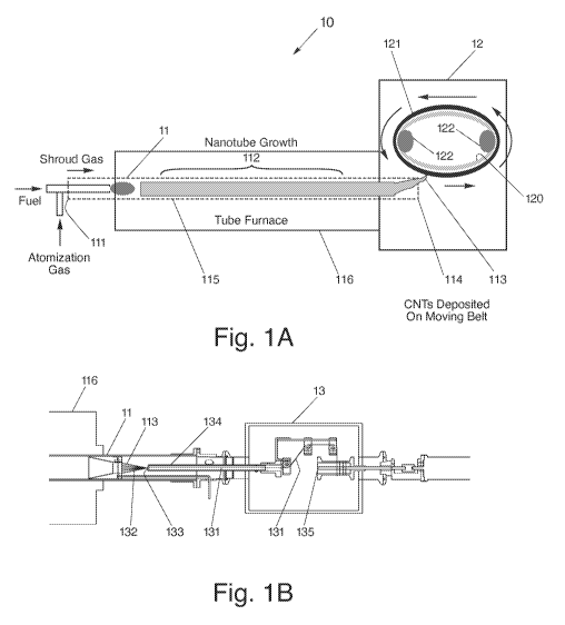
[0038] With reference now to Fig. IA, there is illustrated a system 10,
similar to that
disclosed in U.S. Patent Application Serial No. 11/488,387 filed July 17,
2006,
published February 15, 2007 as U.S. Patent Application No. 20070036709 ('the
"709
Application'), which is incorporated herein by reference, for use in the
fabrication of
nanotubes. System 10, in an embodiment, may be coupled to a synthesis chamber
11.
The synthesis chamber 11, in general, includes an entrance end 111, into which
reaction gases (i.e., gaseous carbon source) may be supplied, a hot zone 112,
where
synthesis of extended length nanotubes 113 may occur, and an exit end 114 from
which the products of the reaction, namely the nanotubes and exhaust gases,
may exit
and be collected. The synthesis chamber 11, in an embodiment, may include a
quartz
tube 115 extending through a furnace 116. The nanotubes generated by system
10, on
the other hand, may be individual single-walled nanotubes, bundles of such
nanotubes, and/or intertwined single-walled nanotubes (e.g., ropes of
nanotubes).
[0039] System 10, in one embodiment of the present invention, may also include
a
housing 12 designed to be substantially airtight, so as to minimize the
release of
potentially hazardous airborne particulates from within the synthesis chamber
11 into
the environment. The housing 12 may also act to prevent oxygen from entering
into
the system 10 and reaching the synthesis chamber 11. In particular, the
presence of
oxygen within the synthesis chamber 11 can affect the integrity and compromise
the
production of the nanotubes 113.
[0040] System 10 may also include a moving belt 120, positioned within housing
12,
designed for collecting synthesized nanotubes 113 made from a CVD process
within
synthesis chamber 11 of system 10. In particular, belt 120 may be used to
permit
nanotubes collected thereon to subsequently form a substantially continuous
extensible structure 121, for instance, a non-woven sheet. Such a non-woven
sheet
may be generated from compacted, substantially non-aligned, and intermingled
nanotubes 113, bundles of nanotubes, or intertwined nanotubes (e.g., ropes of
nanotubes), with sufficient structural integrity to be handled as a sheet.
[0041] To collect the fabricated nanotubes 113, belt 120 may be positioned
adjacent
the exit end 114 of the synthesis chamber 11 to permit the nanotubes to be
deposited
on to belt 120. In one embodiment, belt 120 may be positioned substantially
parallel
CA 02767522 2012-01-06
WO 2011/005964 PCT/US2010/041374
9
to the flow of gas from the exit end 114, as illustrated in Fig. IA.
Alternatively, belt
120 may be positioned substantially perpendicular to the flow of gas from the
exit end
114 and may be porous in nature to allow the flow of gas carrying the
nanomaterials
to pass therethrough. Belt 120 may be designed as a continuous loop, similar
to a
conventional conveyor belt. To that end, belt 120, in an embodiment, may be
looped
about opposing rotating elements 122 (e.g., rollers) and may be driven by a
mechanical device, such as an electric motor. Alternatively, belt 120 may be a
rigid
cylinder. In one embodiment, the motor may be controlled through the use of a
control system, such as a computer or microprocessor, so that tension and
velocity can
be optimized.
[0042] In an alternate embodiment, instead of a non-woven sheet, the
fabricated
single-walled nanotubes 113 may be collected from synthesis chamber 11, and a
yarn
131 may thereafter be formed as illustrated in Fig. 1B. Specifically, as the
nanotubes
113 emerge from the synthesis chamber 11, they may be collected into a bundle
132,
fed into intake end 133 of a spindle 134, and subsequently spun or twisted
into yarn
131 therewithin. It should be noted that a continual twist to the yarn 131 can
build up
sufficient angular stress to cause rotation near a point where new nanotubes
113 arrive
at the spindle 134 to further the yarn formation process. Moreover, a
continual
tension may be applied to the yarn 131 or its advancement into collection
chamber 13
may be permitted at a controlled rate, so as to allow its uptake
circumferentially about
a spool 135.
[0043] Typically, the formation of the yarn 131 results from a bundling of
nanotubes
113 that may subsequently be tightly spun into a twisting yarn. Alternatively,
a main
twist of the yarn 131 may be anchored at some point within system 10 and the
collected nanotubes 113 may be wound on to the twisting yarn 131. Both of
these
growth modes can be implemented in connection with the present invention.
[0044] In one embodiment, carbon nanotubes created in a furnace may be pulled
along a furnace tube 202 and collected on a take-up reel 210 as shown in Figs.
1C-D.
As shown in the perspective view (Fig. 1C), carbon nanotubes created from the
furnace tube 202 may be pulled along the length of the furnace tube 202 and
impinge
on a cone-shaped anchor 204. The anchor 204 functions similar to that of a
reel in
collecting the carbon nanotubes. The carbon nanotubes may subsequently be
pulled
CA 02767522 2012-01-06
WO 2011/005964 PCT/US2010/041374
from the anchor 204 and directed into a wiggle tube 206 within a spinning box
216
(best shown in the top-down view of Fig. 1D). The wiggle tube is capable of
spinning
the carbon nanotubes into a yarn. The yarn of carbon nanotubes coming off the
wiggle tube 206 may be directed to tension gauges 208 for providing the
necessary
tension to the yarn. In some instances, the tension gauges 208 are capable of
measuring the tension as to indicate to motors 212 how fast to spin in order
to collect
the yarn about the take-up reel 210.
[0045] In this example, a motor 212 controls the wiggle tube 206 through an
extending rod within the spinning box 216. Another motor 212 drives the anchor
204,
the motor 212 being disposed underneath the anchor 204 (best seen in Fig. 1C).
And
another motor 212 controls the spinning speed of the take-up reel 210, the
motor 212
being disposed on a top-side of the spinning box 216 (also best seen in Fig.
1C). The
spinning box 216 further includes a blow-out membrane 214 to mitigate
explosions
within the spinning box 216 itself. A plurality of connectors 218 may also be
disposed about a side of the spinning box 216, the connectors 218 being
capable of
providing inert gas to the system (e.g., helium) and for carrying out oxygen
and
hydrogen measurements with appropriate sensors.
[0046] In some chamber systems, the spinning system provides a false spin on
the
yarn. In other chamber systems, the spinning system provides a true spin on
the yarn.
In some embodiments, the spinning is carried out in line with the yarns coming
off the
system. In other embodiments, the spinning is at 90 degrees with respect to
the yarns
coming off the system.
[0047] One method for generating and growing very large numbers of extended
length carbon nanotubes (CNTs) from a fixed substrate is provided in U.S.
Patent
Application Serial No. 11/035,471 filed January 14, 2005, published August 4,
2005
as U. S. Patent Application No. 20050170089, which is hereby incorporated
herein by
reference. The method includes, among other things, spinning a group of
nanoscale
tubes or fibers into a yarn. Thereafter, the yarn can be collected or further
spun using
conventional fiber processing means. Such an approach, in an embodiment, can
employ any known protocols available in the art, and can be incorporated into
a
manufacturing process of the present invention.
CA 02767522 2012-01-06
WO 2011/005964 PCT/US2010/041374
11
[0048] Another method for manufacturing a conducting member made from a
nanostructure-based material is provided in U.S. Application Serial No.
12/437,537,
filed May 7, 2009, which is hereby incorporated herein by reference.
Conductor
[0049] To carry relatively high current pulses between two movable conductors,
such
as a high energy capacitor, a ground strap, a bus bar or bus pipe, or pulse
generating
circuit, to an external circuit without degradation of the waveform or without
heating
of a junction, the present invention provides, in an embodiment, a conductor
20, such
as that shown in Fig. 2. The conductor 20 can include, among other things, a
conductive nanostructure-based material 21, a connector portion 22, and a
coupling
mechanism 23 made from a material capable of providing substantially low
resistance
coupling, while substantially maximizing the number of conductive
nanostructures
that can be actively involved in conductivity.
[0050] In accordance with one embodiment, the conductor 20 includes a
conducting
member 21 made from a conductive nanostructure-based material. The conductive
nanostructure-based material, in an embodiment, may be yarns, ribbons, wires,
cables,
tapes or sheets (e.g., woven or non-woven sheets) made from carbon nanotubes
fabricated in a manner similar to that disclosed above in the `709
Application. In an
embodiment, conducting member 21 may be made from one of carbon, copper,
silver,
boron-nitride, boron, MoS2, or a combination thereof. Moreover, the material
from
which the conducting member 21 may be made can include, in an embodiment,
graphite of any type, for example, such as that from pyrograph fibers.
[0051] The conductor 20 can also include a connector portion 22 to which the
conducting member 21 may be joined. In one embodiment, the connector portion
22
may be made from a metallic material, such as copper, aluminum, gold, silver,
silver
coated copper, cadmium, nickel, tin, bismuth, arsenic, alloys of these metals,
boron,
boron nitride, a combination thereof, or other materials capable of being
electrically
and/or thermally conductive. The connector portion 22 may also be made from
non-
metallic material, such as those having glassy carbons, ceramics, silicon,
silicon
compounds, gallium arsenide or similar materials, or a combination thereof, so
long
as the material can be electrically and/or thermally conductive. The connector
portion
CA 02767522 2012-01-06
WO 2011/005964 PCT/US2010/041374
12
22, in and embodiment, when coupled to conducting member 21, permits
relatively
high current from a source that may be carried by the conducting member 21 to
be
directed to an external circuit without substantial degradation.
[0052] To do so, the conductor 20 may further include a coupling mechanism 23
situated between the conducting member 21 and the connector portion 22, so as
to
join the conducting member 21 to the connector portion 22. In one embodiment,
the
coupling mechanism 23 may be made from a glassy carbon material capable of
providing substantially low resistance coupling. Glassy carbon, in general,
may be a
form of carbon related to carbon nanotubes and can contain a significant
amount of
graphene like ribbons comprising a matrix of amorphous carbon. These ribbons
include sp2 bonded ribbons that can be substantially similar to the sp2 bonded
nanotubes. As a result, they can have relatively good thermal and electrical
conductivity. Examples of precursor materials from which glassy carbon can be
made
include furfuryl alcohol, RESOL resin (i.e., catalyzed alkyl-phenyl
formaldehyde),
PVA, or liquid resin or any material known to form glassy carbon when heat
treated.
Of course, other commercially available glassy carbon materials or precursor
materials can be used.
[0053] In addition, coupling mechanism 23 may also provide the conducting
member
21 with substantially uniform contact to the connector portion 22 across a
contact
surface area on the connector portion 22. To that end, the coupling mechanism
23 can
act to substantially maximize the number of conductive nanostructures within
the
conducting member 21 that can be actively involved in conductivity to enhance
efficiency of electrical and thermal transport. For instance, relatively high
current
from a source and carried by the conducting member 21 can be directed to an
external
circuit without substantial degradation. The conductor 20 of the present
invention,
thus, can be used to enable efficient conduction to a standard connector for
use in a
traditional electrical and/or thermal circuit systems. In particular,
conductor 20 can
enable efficient interaction, for instance, through electrical and/or thermal
conduction,
between a nanoscale environment and the traditional electrical and/or thermal
circuit
system.
[0054] For comparison purposes, the electrical and thermal conduction
properties for
glassy carbon is compared to those properties exhibited by graphite. As
illustrated in
CA 02767522 2012-01-06
WO 2011/005964 PCT/US2010/041374
13
Table 1 below, the presence of the graphene ribbons can enhance the electrical
and
therefore the thermal conductivity of glassy carbon relative to that observed
with
graphite.
Table 1
parameter Graphite Glassy Carbon
Electrical resistivity 14.70 x 10 ohm-cm 0.50 x 10 ohm-cm
Thermal conductivity 95 w/ m 'K 6.3 w/m K
[0055] In another embodiment, there is provided a method for making a
conductor of
the present invention. The method includes initially providing a conducting
member,
similar to conducting member 21, made from a nanostructure-based material, and
a
connector portion, similar to connector portion 22, to which the conducting
member
may be joined. The nanostructure-based material, in one embodiment, can be
those
made from conductive carbon nanotube, for instance, yarns, tapes, cables,
ribbons, or
sheets made from carbon nanotubes. The connector portion, on the other hand,
may
be made from a metallic material, such as copper, nickel, aluminum, silver,
gold,
cadmium, tin, bismuth, arsenic, alloys of these metals, boron, boron-nitride,
other
conductive metals, any conductive metals coated with gold or silver, or a
combination
thereof. The connector portion may also be made from non-metallic material,
such as
those having glassy carbon forms, ceramics, silicon, silicon compounds,
gallium
arsenide, or similar materials, so long as the material can be electrically
and/or
thermally conductive.
[0056] Next, a coupling mechanism, similar to coupling mechanism 23, may be
placed at a junction between the conducting member and the connector portion.
In an
embodiment, the coupling mechanism may be a glassy carbon precursor, such as
furfuryl alcohol, Resol resin, PVA or any material known to form glassy carbon
when
heat treated that can be deposited into the junction. It should be appreciated
that the
tendency of the glassy carbon resin or material to "wet" the nanotubes in the
conducting member can help to coat each individual nanotube, so that each
nanotube
can contribute to electron or thermal transport.
[0057] The conducting member and connector portion may thereafter be held
against
one another, while the junction between the conducting member and the
connector
portion may be heated to a temperature range sufficient to pyrolyze the glassy
carbon
CA 02767522 2012-01-06
WO 2011/005964 PCT/US2010/041374
14
precursor to form a glassy carbon low resistance coupling mechanism. In one
embodiment, the minimum temperature of pyrolysis should be at least in the
neighborhood of about 400 C to about 450 C. If pyrolysis is carried out in
an inert
atmosphere, the temperature may need to be higher to permit the pyrolysis
process to
go to completion.
[0058] It should be appreciated that materials that may be sensitive to this
temperature may not be suitable for this invention. Moreover, pyrolysis need
not go
to completion for this junction to offer substantially superior contact
resistance to the
traditional means for coupling conducting members.
[0059] Looking now at Fig. 3, in accordance with another embodiment of the
present
invention, there is shown a conductor 30, for carrying relatively high current
from a
source to an external circuit without substantial degradation of the waveform
or
without substantially heating of a junction.
[0060] In the embodiment shown in Fig. 3, conductor 30 includes a conducting
member 31 made from a conductive nanostructure-based material. The conductive
nanostructure-based material, in an embodiment, may include yarns, ribbons,
cables,
tapes or sheets (e.g., woven or non-woven sheets) made from carbon nanotubes
fabricated in a manner similar to that disclosed above in the `709
Application. In an
embodiment, conducting member 31 may be made from one of carbon, copper,
silver,
boron-nitride, boron, MoS2, or a combination thereof. The material from which
the
conducting member 31 may be made can also include, in an embodiment, graphite
of
any type, for example, such as that from pyrograph fibers.
[0061] Conductor 30, as illustrated, can also include a connector portion 32
at each of
opposing ends of the conducting member 31. In one embodiment of the invention,
connector portion 32 may be a coating deposited, such as electroplating,
directly on
each end of conducting member 31. Deposition or electroplating of connector
portion
32 on to conducting member 31 can be carried out using methods well known in
the
art. Examples of electroplated connector portion 32 include gold, silver,
nickel,
aluminum, copper, bismuth, tin, zinc, cadmium, tin-nickel alloy, copper alloy,
tin-zinc
alloy, bismuth-copper alloy, cadmium-nickel alloy, other conductive metals and
their
alloys, or a combination thereof.
CA 02767522 2012-01-06
WO 2011/005964 PCT/US2010/041374
[0062] Connector portion 32, in an embodiment, may be deposited or
electroplated on
to conducting member 31 substantially uniformly, so as to permit substantially
uniform contact of the nanotubes in conducting member 31 across a contact
surface
area on the connector portion 32. As such, the connector portion 32 can act to
substantially maximize the number of conductive nanostructures within the
conducting member 31 that can be actively involved in conductivity to enhance
efficiency of electrical and thermal transport and reduce contact resistance.
To that
end, relatively high current from a source and carried by the conducting
member 31
can be directed to an external circuit without substantial degradation. The
conductor
30, thus, can be used to enable efficient interaction, for instance, through
electrical
and/or thermal conduction, between a nanoscale environment and the traditional
electrical and/or thermal circuit system, as well as conduction to a standard
connector
for use in a traditional electrical and/or thermal circuit systems.
[0063] With reference now to Figs. 4A-B, in accordance with a further
embodiment
of the present invention, an conductor 40 can be designed to extend or expand
in at
least one direction, for instance, lengthwise, without compromising or
substantially
changing the resistivity of the conductor 40. In other words, resistivity or
the
resistance property of the conductor 40 can be independent of extension or
expansion
of conductor 40, even if the extension or expansion is to a substantially
extreme
degree.
[0064] Conductor 40, in one embodiment, includes a conducting member 41 made
from a conductive nanostructure-based material. Such a material may be a sheet
(e.g.,
woven or non-woven sheet) a plurality of tapes or ribbons made from carbon
nanotubes, similar in manner to that disclosed in the `709 Application.
Moreover, the
material from which the conducting member is made may include, in an
embodiment,
graphite of any type, for example, such as that from pyrograph fibers.
[0065] However, unlike conductor 30 shown in Fig. 3, conducting member 41 of
conductor 40 may be imparted or etched with various patterns, including that
shown
in Figs. 4A and 4B to permit the conductor 40 to extend or expand, for
instance, in a
lengthwise direction (i.e., along the X axis) when pulled axially from
opposite ends of
the conductor 40 (see Fig. 4B). It should be appreciated that in addition to
the
patterns shown in Figs. 4A and 4B, the conducting member 41 may include other
CA 02767522 2012-01-06
WO 2011/005964 PCT/US2010/041374
16
patterns or designs, so long as such a pattern or design permits extension of
conductor
40.
[0066] Although shown extending in a lengthwise direction, conductor 40 may
also
be designed to extend along its width (i.e., along the Y axis). As shown in
Figs. 4C-
D, conducting member 41 may be provided with any pattern known in the art that
allows the conductor 40 to extend or be extensible along its width. It should
be
appreciated that conducting member 41 may also include a pattern that allows
the
conductor 40 to extend lengthwise as well as along its width (i.e., in two
dimensions).
[0067] To the extent desired, looking now at Fig. 4E, conductor 40 may include
two
or more layers of conducting member 41, one on top of the other, and
substantially
non-bonded to one another, along their length, so that conductor 40 may also
be
extendible along the Z axis. In such an embodiment, conducting members 41 may
be
bonded to one another along their respective edges 43. In an embodiment
bonding of
the edges 43 can be accomplished by the use of a glassy carbon material, such
as that
provided above.
[0068] In addition to being extendible, conducting member 41 may also be
provided
with shape memory capability. Specifically, the nanotubes from which
conducting
member 41 may be made can permit the conducting member 41 to retract
substantially back to its originally length, width or shape (see Fig. 4A)
after the
conducting member 41 has been extended (see Fig. 4B) along one, two or three
dimensions.
[0069] The pattern, design or etching provided on conducting member 41, in an
embodiment, may be implement by processes known in the art, include stamping,
laser etching etc.
[0070] The conductor 40 can also include a connector portion 42 at each of
opposing
ends of the conducting member 41. In one embodiment of the invention,
connector
portion 42 may be a coating deposited, such as by electroplating, directly on
each end
of conducting member 41. Deposition or electroplating of connector portion 42
on to
conducting member 41 can be carried out using methods well known in the art.
In
one embodiment, the connector portion 42 may be made from a metallic material,
such as gold, silver, nickel, aluminum, copper, bismuth, tin, zinc, cadmium,
tin-nickel
alloy, copper alloy, tin-zinc alloy, bismuth-copper alloy, cadmium-nickel
alloy, other
CA 02767522 2012-01-06
WO 2011/005964 PCT/US2010/041374
17
conductive metals and their alloys, or a combination thereof. The connector
portion
42 may also be made from non-metallic material, such as those having glassy
carbon
forms, or similar materials, so long as the material can be electrically
and/or thermally
conductive. To the extent that the conductor 40 may be designed to allow
conducting
member 41 to extend or be extensible along its width, similar to that shown in
Fig.
4D, connector portion 42 may also be designed to extend or be extensible
widthwise
along with the conducting member 41.
[0071] In accordance with one embodiment, connector portion 42 may be
deposited
or electroplated on to conducting member 41 substantially uniformly to permit
substantially uniform contact of the nanotubes in conducting member 41 across
a
contact surface area on the connector portion 42. To that end, the connector
portion
42 can act to substantially maximize the number of conductive nanostructures
within
the conducting member 41 that can be actively involved in conductivity to
enhance
efficiency of electrical and thermal transport. The conductor 40 of the
present
invention can be used to enable efficient interaction, for instance, through
electrical
and/or thermal conduction, between a nanoscale environment and the traditional
electrical and/or thermal circuit system, as well as conduction to a standard
connector
for use in a traditional electrical and/or thermal circuit systems.
[0072] Conductors 20, 30 and 40 may be used as current conducting members,
including high current conducting members, capacitors, battery electrodes,
fuel cell
electrodes, as well as for thermal transport, for high frequency transport,
and many
other applications. With respect to conductor 40, because of its ability to
extend, its
shape memory capability, as well as its thermal and electrical conductive
properties,
conductor 40 may be used for a variety of structural and mechanical
applications,
including those in connection with the aerospace industry, for example, as a
conducting member on modern airplane wings that have curved up designs.
Hybrid Conductors
[0073] Hybrid conductors capable of achieving enhanced conductivity and
current
capacity over a wide range of frequencies are disclosed. One method of
fabricating
such hybrid conductors includes contacting a conductive material (e.g.,
silver, gold,
copper) with a plurality of nanostructures. In some instances, the conductive
material
CA 02767522 2012-01-06
WO 2011/005964 PCT/US2010/041374
18
enhances electrical and/or thermal conductivity along the plurality of
nanostructures.
In one embodiment, the plurality of nanostructures is a yarn of nanotubes. In
another
embodiment, the plurality of nanostructures is a sheet of nanotubes. In some
embodiments, the plurality of nanostructures includes nanotubes made from one
of
carbon, copper, silver, boron, boron-nitride, or a combination thereof. The
nanostructures may also include other types of nanotubes disclosed herein.
Generally,
the contacting involves only a portion of the surface of the plurality of
nanostructures.
For example, by utilizing a plurality of nanostructures, some portions of the
periphery
of adjacent nanostructures may not be in physical contact with the conductive
material
but would instead be in contact with another nanostructure.
[0074] In one embodiment, a hybrid conductor can be produced, the hybrid
conductor
having: a plurality of nanostructures, wherein each nanostructure has a
surface area; a
member having a geometric profile defined by the plurality of nanostructures;
and a
conductive material positioned so that it is in contact with less than the
total surface
area of the plurality of nanostructures, wherein the combination of the
conductive
material and the plurality of nanostructures enhances conductivity while
decreasing
resistivity along the length of the member. As used herein, less than the
total surface
area and the like means not 100%. In some embodiments, the contact between the
conductive material and the total surface area of the plurality of
nanostructures may
be not greater than about 95%, or not greater than about 90%, or not greater
than
about 85%, or not greater than about 80%, or not greater than about 75%, or
not
greater than about 70%, or not greater than about 65%, or not greater than
about 60%,
or not greater than about 55%, or not greater than about 50%. In other
embodiments,
the conductive material includes one of a conductive coating in contact with
less than
the total surface area of the plurality of nano structures, a conductive wire
in contact
with less than the total surface area of the plurality of nanostructures, or a
combination thereof. In one embodiment, the member defined by the plurality of
nanostructures includes one of a yarn or a sheet. In some embodiments, the
member
includes one of a plurality of yarns, a plurality of sheets, or a combination
thereof.
[0075] In one instance, contacting includes intertwining or interweaving two
different
materials (e.g., a plurality of nanostructures and a copper wire, a plurality
of
nanostructures and an aluminum wire). In another embodiment, contacting
includes
coating and/or depositing one material onto another (e.g., electroplating
copper onto a
CA 02767522 2012-01-06
WO 2011/005964 PCT/US2010/041374
19
plurality of nanostructures, physical vapor depositing copper onto a plurality
of
nanostructures). In some instances, contacting includes placing or positioning
two
materials in physical contact. In some embodiments, the contacting may produce
a
composite or hybrid product.
[0076] In one example, carbon nanotubes may be contacted with a copper wire to
produce a hybrid conductor. In some embodiments, a yarn of carbon nanotubes
may
be contacted with a gold wire to produce a composite conductor. In some
instances,
the carbon nanotubes may be fabricated according to the techniques disclosed
in the
present application. In one embodiment, a hybrid conductor includes metallic
and
nanostructure materials. In other embodiments, the hybrid conductor includes
non-
metallic and nanostructure materials. In some embodiments, the conductive
material
includes at least one of copper, aluminum, titanium, platinum, nickel, gold,
silver, or a
combination thereof.
[0077] One embodiment discloses a hybrid conductor having a plurality of
nanostructures coupled and a conductive material circumferentially deposited
about
the plurality of nanostructures so as to enhance conductivity along the
plurality of
nanostructures. In one embodiment, the plurality of nanostructures comprises a
yarn
of nanotubes. In some embodiments, the nanostructures may be made produced
from
one of carbon, copper, silver, boron, boron-nitride, MoS2 or similar
compounds, or a
combination thereof.
[0078] In some embodiments, the plurality of nanostructures may be doped in a
solution having one of FeC13, SbC13, Sb13, SbF3, SbC15, Bi(N03)3, TeCI4,
CuSO4,
CuC12, HC1, NaCl, NaSO4, Fe(N03)3, hydronium ion, hydrochloric acid,
hydrobromic
acid, hydrofluoric acid, hydroiodic acid, carbonic acid, sulfuric acid, nitric
acid,
fluorosulfuric acid, chlorosulfonic acid, methane sulfonic acid,
trifluoromethane
sulfonic acid, oleum, an agent thereof, or a combination thereof. The doping
of
nanotubes will become more apparent in subsequent discussion. In other
embodiments, the plurality of nanostructures may be doped in a solution having
one
of fluoride salt, chloride salt, bromide salt, iodate salt, nitrate salt,
sulfate salt, or a
combination thereof.
[0079] In some embodiments, the conductive material may be made from one of
copper, aluminum, titanium, platinum, nickel, gold, silver, silver coated
copper,
CA 02767522 2012-01-06
WO 2011/005964 PCT/US2010/041374
cadmium, nickel, tin, bismuth, arsenic, alloys of these metals, boron, boron
nitride,
glassy carbon, ceramics, silicon, silicon compounds, gallium arsenic, a
combination
thereof, or other materials capable of being electrically and/or thermally
conductive.
[0080] In one embodiment, the conductive material may be coated on the
plurality of
nanostructures. In one instance, coated means covering a first object with a
second
object. For example, the first object may be a plurality of carbon nanotubes
and the
second object may be a metallic, semi-metallic or a non-metallic layer. The
metallic,
semi-metallic or non-metallic layer may partially cover the plurality of
carbon
nanotubes. In another example, the first object may be a plurality of carbon
nanotubes in the form of a wire and the second object may be a copper film
that
substantially encapsulates the wire. In yet another example, the first object
may be a
plurality of carbon nanotubes and the second object may be a layer of gold
film,
which substantially encapsulates the carbon nanotubes. In another embodiment,
the
plurality of nanostructures may be a sheet of nanotubes coated with a
conductive
material such as a gold or copper film.
[0081] In one embodiment, the conductive material may be deposited on the
conductive members. In one instance, deposited means laying down a layer of
material on the surface of an object, the material being different than the
object. In
some embodiments, techniques include electroplating or electroless plating,
among
others, may be used for depositing the conductive material onto the plurality
of
nanostructures. In one embodiment, a hybrid conductor may be formed by
electroplating a transition metal (e.g., copper) onto a strip of carbon
nanotubes. In
this instance, the strip of carbon nanotubes may be similar to a bundle or
yarn of
nanotubes. In one example, the transition metal may be deposited directly on
the
carbon nanotubes. In another example, a seed layer (e.g., nickel) may be
deposited on
the strip of carbon nanotubes followed by electroplating of the transition
metal
material. In another instance, the conductive material may be deposited onto a
sheet
of nanotubes via electroplating or physical vapor deposition, among other
techniques.
In some embodiments, the transition metal includes elements and/or alloys of
silver,
copper, gold, aluminum, titanium, platinum, nickel, or alloys or combinations
thereof.
[0082] In one embodiment, the hybrid conductor is designed to enable efficient
conduction between a nanoscale environment and a traditional electrical and/or
thermal circuit system. In another embodiment, the conductive material of the
hybrid
CA 02767522 2012-01-06
WO 2011/005964 PCT/US2010/041374
21
conductor is capable of enabling relatively high current from a source and
carried by
the bundle to be directed to an external circuit without substantial
degradation.
[0083] In some embodiments, the hybrid conductor is designed for use in one of
thermal conduction, electrical conduction, EMI applications, high current
transmission, RF applications, pulsed applications, thermo-electric and/or
power
generation, sensor applications, or other similar applications. In other
embodiments,
the hybrid conductor is designed to enable efficient conduction to a standard
connector for use in traditional electrical and/or thermal circuit systems.
[0084] In some instances, hybrid conductors may be incorporated as electrical
or
thermal conductors, among others. In other instances, hybrid conductors
include
without limitation electrical or optical wires or cables including coaxial
cables, cable
wires, universal serial bus (USB) cables. In some embodiments, hybrid
conductors
may include any electrical or thermal conductors requiring high current
capacity and
conductivity while operating over a wide range of frequencies (e.g., from DC
to GHz)
and/or a wide range of temperatures (e.g., from about < 0 C to not less than
about
200 C).
[0085] In one instance, the conductive member and the conductive material may
be
placed or positioned in physical contact with one another (e.g., physically
interwoven). In one embodiment, the plurality of nanostructures and the
conductive
material may be physically coupled to each other as to form a geometric
pattern. In
some embodiments, coupling techniques may include twining, braiding, winding,
and
plying, to name a few. In one example, twining means twisting together a yarn
of
carbon nanotubes and the conductive member to form an interwoven pattern. In
another example, winding means coiling the conductive member around a sheet of
carbon nanotubes, or vice versa, to form a coiled pattern. In yet another
example,
braiding means twisting together the sheet of carbon nanotubes and the
conductive
member into a spiral shape. In some instances, the conductive material (e.g.,
gold or
aluminum) may be electroplated onto the yarn or sheet of carbon nanotubes.
[0086] In some embodiments, the plurality of nanostructures may be carbon
nanotubes in the form of a strip, a wire, a sheet, a yarn, or a combination
thereof. In
one embodiment, the plurality of nanostructures may be in the form of a strip
(e.g.,
any length or width up to about 2 mm in thickness). In one embodiment, the
plurality
of nanostructures may be in the form of a wire (e.g., any length and up to
about 20
CA 02767522 2012-01-06
WO 2011/005964 PCT/US2010/041374
22
mm in diameter). In some embodiments, the plurality of nanostructures may be
in the
form of a strip and a wire, two strips, two wires, or any combinations
thereof. In
another embodiment, the plurality of nanostructures may be a sheet of carbon
nanotubes.
[0087] In one embodiment, a hybrid wire conductor may be electroplated in a
similar
fashion to that of a hybrid strip conductor. In another embodiment, a hybrid
wire
conductor may be produced by plying or braiding several individual strands of
carbon
nanotubes together with a metal wire (e.g., from about 30 to about 50 AWG).
The
geometric pattern formed as a result of the braiding can be modified to allow
the
metal wire to move from the inside to the outside (e.g., similar to a Litz
wire as
described herein), or as a core conductor with carbon nanotubes wrapping
around the
core conductor. This will become more apparent in subsequent figures and
discussion.
[0088] In one embodiment, carbon nanotubes may undergo treatment to enhance
conductivity and productivity of the carbon nanotubes. In these instances, the
carbon
nanotubes may be one of sheet, strip, wire, yarn, or combinations thereof. For
carbon
nanotube sheets, enhanced conductivity and productivity may result from a
treatment
process. Likewise, if nanotube strips are generated, the strips may also
undergo a
treatment processes to enhance conductivity and productivity of the nanotubes
in the
strip. Treatment of a composite sheet after formation may, in an embodiment,
include
subjecting the composite sheet to a protonation agent. One feature of the
protonation
agent may be to bring the carbon nanotubes in closer proximity with one
another. By
bringing the carbon nanotubes closer together, the protonation agent may act
to
reduce surface tension, reduce resistivity, and increase conductivity of the
sheet.
[0089] Examples of a protonation agent may include an acid such as hydronium
ion,
hydrochloric acid, hydrobromic acid, hydrofluoric acid, hydroiodic acid,
carbonic
acid, sulfuric acid, nitric acid, fluorosulfuric acid, chlorosulfonic acid,
methane
sulfonic acid, trifluoromethane sulfonic acid, oleum, an agent thereof, or a
combination thereof, or other materials capable of being electrically and/or
thermally
conductive. In other embodiments, the plurality of nanostructures may be doped
in a
solution having one of fluoride salt, chloride salt, bromide salt, iodate
salt, nitrate salt,
sulfate salt, or a combination thereof. In these embodiments, doping includes
CA 02767522 2012-01-06
WO 2011/005964 PCT/US2010/041374
23
immersing and/or submerging the nanostructures in a solution for a
predetermined
temperature and time. Although the doping is performed on sheet of carbon
nanotubes, the doping process may also be performed on yarns and strips of
carbon
nanotubes, among others.
[0090] In some embodiments, the solution may include a solvent, a polymer, a
metal,
or a combination thereof. The solvent used in connection with the solution of
the
present invention can be used to lubricate the sheet in order to gain better
alignment
and enhancement in the properties of the carbon nanotubes. Examples of a
solvent
that can be used in connection with the solution include toluene, kerosene,
benzene,
hexanes, any alcohol including but not limited to ethanol, methanol, butanol,
isopropanol, as well as tetrahydrofuran, 1-methyl-2-pyrrolidinone, dimethyl
formamide, methylene chloride, acetone or any other solvent as the present
invention
is not intended to be limited in this manner. In an embodiment, the solvent
may be
used as a carrier for a polymer, monomer, inorganic salt, or metal oxide to.
[0091] Examples of a polymer that can be used in connection with the solution
include a small molecule or polymer matrix (thermoset or thermoplastic)
including,
but not limited to, polyurethane, polyethylene, poly(styrene butadiene),
polychloroprene, poly(vinyl alcohol), poly(vinyl pyrrolidone),
poly(acrylonitrile-co-
butadiene-co-styrene), epoxy, polyureasilazane, bismaleimide, polyamide,
polyimide,
polycarbonate, or any monomer including styrene, divinyl benzene, methyl
acrylate,
and tert-butyl acrylate. In an embodiment, the polymer may include polymer
particles, that are difficult to obtain in liquid form.
[0092] Examples of a metal that can be used in connection with the solution
include a
salt (any transition metal, alkali metal, or alkali earth metal salt or
mixture thereof
including, but not limited to, nickel hydroxide, cadmium hydroxide, nickel
chloride,
copper chloride, calcium zincate (CaZn2(OH)6)), or metal oxide (any transition
metal,
alkali metal, or alkali earth metal oxide or mixture thereof, including but
not limited
to: zinc oxide, iron oxide, silver oxide, copper oxide, manganese oxide,
LiCoO2,
LiNiO2, LiNi,,Coi_XO2, LiMn2O4). In an embodiment, the metal may include
polymers or volatile solvents to create a carbon nanotube metal matrix
composite.
Examples of such polymers or volatile solvents include powdered forms of
aluminum
or its alloys, nickel, superalloys, copper, silver, tin, cobalt, iron, iron
alloys, or any
CA 02767522 2012-01-06
WO 2011/005964 PCT/US2010/041374
24
element that can be produced in a powdered form including complex binary and
ternary alloys or even superconductors.
[0093] Another embodiment discloses contacting a conductive wire with a
portion of
the surface of the conductive material and the plurality of nanostructures. In
some
embodiments, the conductive wire maybe copper, aluminum, titanium, nickel,
gold,
silver, or a combination thereof. For example, a copper wire may be
intertwined with
the hybrid conductive material and nanostructures. In this instance, the
copper wire
may help to enhance conductivity (e.g., electrical, thermal) of the plurality
of
nanostructures similar to those described above. In one embodiment, a sheet of
carbon nanotubes may be contacted with a conductive material such as a copper
film.
The hybrid sheet of copper and carbon nanotubes may then be contacted with a
plurality of aluminum wires for enhanced conductivity (e.g., electrical,
thermal) of the
hybrid sheet of carbon nanotubes. A plurality of these hybrid sheets or
various
combinations thereof may be placed adjacent one another to provide an enhanced
hybrid conductor.
[0094] Another embodiment discloses a hybrid conductor having a plurality of
nanostructures, whereby the plurality of nanostructures may be doped for
increased
conductivity. In some embodiments, the nanostructures may be immersed in a
solution including one of FeC13, SbC13, Sb13, SbF3, SbC15, Bi(N03)3, TeC14,
CuSO4,
CuC12, Fe(N03)3, or combinations thereof. In other embodiments, the
nanostructures
may be immersed in a solution including one of chloride salts (e.g., HC1,
NaCl,
CuC12), nitrate salts (e.g., Bi(N03)3), sulfate salts (e.g., CuSO4, NaSO4), or
combinations thereof. The doping may be p-type, n-type, cathodic, anodic, or
combinations thereof. In one instance, the doping may be carried out in
conjunction
with the deposition and/or coating techniques disclosed herein. In other
instances, the
doping may be carried out by itself in fabricating the hybrid conductor. In
other
embodiments, the solution may include those described herein.
[0095] In some instances, the doping or immersion solution may be prepared by
mixing about 10 wt. % solutions of the salts disclosed herein in a solvent or
mixture
of solvents (e.g., water, acetone, ethanol, toluene), and immersing (e.g.,
soaking) the
carbon nanotubes in the solution for about one hour. For example, a plurality
of
carbon nanotubes may be doped in a CuSO4 solution by soaking or immersing them
in
CA 02767522 2012-01-06
WO 2011/005964 PCT/US2010/041374
a CuSO4 solution for a predetermined amount of time and at a predetermined
temperature. The immersed samples may be dried at about 120 C for about one
hour
to produce the doped carbon nanotubes. As discussed, the doping may be carried
out
with or without the contacting step (e.g., deposition and/or coating
techniques). In
some embodiments, different concentration of solutions may be utilized. For
example, the carbon nanotubes may be doped in about 50 wt. % nitric acid
solution
for not less than about 5 seconds. In other instances, the carbon nanotubes
may be
doped in about 40 wt. % salt solution, or about 30 wt. % salt solution, or at
least about
10 wt. % salt solution, or not greater than about 90 wt. % salt solution. In
some
embodiments, the soaking or immersion time may be at least about 5 seconds, or
at
least about 10 seconds, or at least about 30 seconds, or at least about 1
minute, or not
greater than 10 minutes, or not greater than 5 minutes.
[0096] Additional details on doping carbon nanotubes are provided in U.S.
Patent
Application Serial No. 12/437,538 filed May 7, 2009, which is hereby
incorporated
herein by reference in its entirety. The method includes, among others, a
nanostructured sheet having a substantially planar body, a plurality of
nanotubes
defining a matrix within the body, and a protonation agent dispersed
throughout the
matrix of nanotubes for enhancing proximity of adjacent nanotubes to one
another.
Such an approach, in an embodiment, can employ any known protocols available
in
the art, and can be incorporated into a fabrication process of the present
invention.
[0097] Another method for doping carbon nanotubes (CNTs) is provided in U.S.
Patent Application Serial No. 12/191,765 filed August 14, 2008, published
February
19, 2009 as U. S. Patent Application No. 20090044848, which is hereby
incorporated
herein by reference in its entirety. The method includes, among other things,
reducing
resistivity and increasing conductivity of the nanotube sheets or yarns by
introducing
trace amounts of foreign atoms (e.g., doping) during the nanotube growth
process.
The method also includes doping nanotube thermal element with one of a p-type
dopant, n-type dopant, or both. Such an approach, in an embodiment, can employ
any
known protocols available in the art, and can be incorporated into a growth
process of
the present invention.
CA 02767522 2012-01-06
WO 2011/005964 PCT/US2010/041374
26
[0098] Yet another method for doping carbon nanotubes (CNTs) is provided in
U.S.
Patent Application Serial No. 12/437,535 filed May 7, 2009, which is hereby
incorporated herein by reference in its entirety.
[0099] In some embodiments, carbon nanotube conductors (e.g., with or without
doping) having electroplated metal may be placed in parallel operation with
carbon
nanotube conductors without any doping and without any electroplated metal for
maximizing conductivity over an entire range of frequency from DC to GHz
(e.g.,
from about 50 Hz up to about 200 MHz). In other embodiments, carbon nanotube
conductors (e.g., with or without doping) without electroplated metal may be
placed
in parallel operation with carbon nanotube conductors without any doping and
without any electroplated metal for maximizing conductivity over a range of
frequency. In yet other embodiments, combinations thereof (e.g., carbon
nanotube
conductors without doping, carbon nanotube conductors with doping,
electroplated
carbon nanotube conductors without doping, electroplated carbon nanotube
conductors with doping) may be incorporated. In some instances, conductors may
be
operated in series with other conductors. In other instances, the conductor
combinations may include transitional metal wires (e.g., copper wire, aluminum
wire). For example, a carbon nanotube strip may be braided or plied with a
copper
wire, or two gold wires, or combinations thereof. In other examples, two
carbon
nanotube wires may be braided or plied with a gold wire, or two copper wires,
or
combinations thereof.
[00100] In some instances, electrons may travel through the metal portion or
the
conductive member (e.g., metal wire) of a conductor at lower frequencies, and
move
to the carbon nanotube portion when operating at higher frequencies (e.g.,
above
MHz). Therefore, weight savings may be realized at lower frequencies by
incorporating the conductive member or metal wire, while the capacitive
coupling
behavior of carbon nanotubes are realized at higher frequencies.
Examples
[00101] Reference is now made to Figs. 5A-5C illustrating a top-schematic
view, side-
schematic view, and actual top-down view of a carbon nanotube strip 502 coated
with
copper 504. In this sample 500, a thin layer of nickel (not visible) was
CA 02767522 2012-01-06
WO 2011/005964 PCT/US2010/041374
27
electrodeposited on both sides of the carbon nanotube strip 502 followed by a
thicker
layer of copper 504, whereby the thickness of the copper metal 504 on either
side of
the strip 502 is about 20 microns.
[00102] This sample 500, along with other similar samples, were subsequently
tested
for resistance as a function of frequency and current capacity at a maximum
temperature of about 300 C. As illustrated in Table 2 below, measurements of
thickness, current and current capacity were carried out on five different
samples.
The raw samples (raw 1, raw 2 and raw 3) were coated with copper on the ends
of the
strips to reduce contact resistance. As shown by the results, the copper
coated
samples (copper coated 1 and copper coated 2) may achieve higher current
capacities
if the temperature may be increased up to about 300 C with higher current.
Table 2 (t system limited to 25 A)
Sample Current Temperature Current Capacity
Raw 1 5.52 A 300 C 4.7 x 10⁶ A/m2
(47 microns thick)
Raw 2 7.51 A 300 C 4.1 x 10⁶ A/m2
(73 microns thick)
Raw 3 4.51 A 342.5 C 5.3 x 10⁶ A/m2
(34 microns thick)
Copper Coated 1 25 A 57.2 C 13.5 x 10⁶ A/m2t
(74 microns thick)
Copper Coated 2 25 A 31.3 C 11.2 x 10⁶ A/m2t
(89 microns thick)
[00103] The copper coated samples were also tested for resistance as a
function of
frequency from DC to about 200 MHz. Reference is now made to Fig. 6
illustrating
resistance per linear density as a function of frequency for a condensed
carbon
nanotube ribbon conductor (A), a copper coated carbon nanotube ribbon
conductor
(C), and a parallel combination of the two (B) versus a pure copper strip
reference
sample (E).
[00104] The condensed carbon nanotube ribbon conductor (A) has a length of
about 10
cm, width of about 0.9 cm, thickness of about 28 microns, and a mass of about
0.03564 gram. The copper coated nanotube ribbon conductor (C) has a length of
about 9.8 cm, width of about 1 cm, thickness of about 106 microns, and a mass
of
about 0.11465 gram. The copper strip reference sample (E) has a length of
about 18.3
CA 02767522 2012-01-06
WO 2011/005964 PCT/US2010/041374
28
cm, width of about 3.3 mm, thickness of about 50 microns, and a mass of about
0.29703 gram.
[00105] As shown, the measured frequency response of the resistance, taking
mass and
size into account, of a raw (e.g., uncoated or untreated) copper nanotube
strip (A)
shows roll-off behavior at around about 10 KHz, which may be attributed to
capacitive coupling, and continues to exhibit a decrease in resistance until
at about 30
MHz, where it then begins to increase. In contrast, copper coated hybrid
samples (B,
C) were able to mimic that of a copper strip (E) until the roll-off point at
which time it
becomes less restrictive (e.g., more conductive) than the copper strip (E) for
the rest
of the measurement up to about 200 MHz.
[00106] Reference is now made to Fig. 7 showing a carbon nanotube wire plied
with
an approximately 40 AWG bare copper wire. In this example, a conductor is
composed of six carbon nanotube wires coupled to one copper wire. In this
instance,
the performance may be similar to that of a copper coated carbon nanotube
strip
conductor as disclosed above, but with a different geometric pattern.
[00107] Reference is now made to Fig. 8 showing a conductor including a copper
coated carbon nanotube wire. In this example, a 150-ply carbon nanotube wire
has
been coated with copper on the ends of the wire.
[00108] Reference is now made to Fig. 9 illustrating measured frequency
analysis
response from about 50 Hz to about 200 MHz of a copper-carbon nanotube hybrid
conductor (A), a carbon nanotube conductor (B), and aluminum (C) and copper
(D)
wires at various temperatures. All the samples in the figure have the same
cross-
sectional area and the specific conductivity is a measure of conductivity
divided by
material density.
[00109] As shown, aluminum (C) and copper (D) samples experience decreases in
specific conductivities with increasing frequency across all temperatures. The
drop-
off for the metal samples appear to begin at about 1 MHz. In addition, the
metal
samples also seem to exhibit decreases in specific conductivities with
increasing
temperatures at each and every frequencies tested. For example, the specific
conductivity of aluminum at 20 C is slightly higher than that of aluminum at
100 C,
which is slightly higher than that of aluminum at 200 C. This is evident
across all
frequencies tested. Similar trend may also be said for copper.
CA 02767522 2012-01-06
WO 2011/005964 PCT/US2010/041374
29
[00110] In contrast, the un-coated or un-treated carbon nanotube (B), having
lower
specific conductivity than the metal samples at lower frequencies (less than
about 100
KHz), appears to exhibit an increase in specific conductivity over metal
samples
beginning at about 3 MHz and continues at higher frequencies. Likewise, the
copper-
carbon nanotube hybrid conductor (A), having lower specific conductivity than
aluminum at 20 C at lower frequencies (less than about 100 KHz), also appears
to
exhibit increasing specific conductivity with increasing frequency starting at
about
100 KHz and continues at higher frequencies. Furthermore, the copper-carbon
nanotube hybrid conductor (A) appears to exhibit higher specific
conductivities than
copper wires (D) at both 100 C and 200 C across all frequencies. This seems
to
suggest that hybrid conductors as disclosed herein may outperform copper or
other
metal wires at higher temperatures across all frequencies. In some
embodiments, the
hybrid conductors may be frequency independent. In other embodiments, the
hybrid
conductors are capable of achieving better performance than metal wires at
frequencies of at least about 1 KHz, or at least about 10 KHz, or at least
about 100
KHz, or at least about 1 MHz, or at least about 10 MHz, or at least about 100
MHz, or
at least about 1 GHz, or at least about 2 GHz, or at least about 5 GHz, or at
least about
GHz. In some embodiments, the hybrid conductors may achieve better
performance than copper or aluminum wires at a wide range of frequency, or
over an
entire range of frequency, or over all frequencies, or independent of
frequency, or a
combination thereof. Similarly, the hybrid conductors may achieve these
performances at various temperatures and across all temperature ranges.
[00111] Although the carbon nanotube materials (A, B) are tested at ambient
temperature (about 20 C), similar performance would have been observed at
elevated
temperatures (e.g., 100 C or 200 C) because the material properties of
carbon
nanotubes are not as temperature sensitive.
[00112] Reference is now made to Fig. 10 illustrating measured frequency
analysis
response from about 50 Hz to about 200 MHz of an acid-treated carbon-nanotube
sheet hybrid conductor. In this instance, the acid-treated carbon-nanotube
hybrid
conductor was treated in approximately 50 wt. % nitric acid solution at
ambient
temperature (e.g., 20 C) for at least about 5 seconds. The acid-treated
carbon-
nanotube hybrid conductor appears to exhibit decreasing impedance with
increasing
frequency. Specifically, the fall-off in impedance begins at about 10 KHz and
CA 02767522 2012-01-06
WO 2011/005964 PCT/US2010/041374
continues with increasing frequencies and appears to taper out at about 1 MHz.
This
may be an indication that the hybrid conductor may provide enhanced
performance
(lower impedance) at higher frequencies. Although this hybrid conductor is in
sheet
form, it is also possible to produce the hybrid conductor in any format
disclosed
herein.
[00113] Reference is now made to Fig. 11 illustrating frequency analysis
responses of
a modeled acid-treated carbon-nanotube hybrid conductor (A), a measured acid-
treated carbon-nanotube hybrid conductor (B), a modeled copper sheet (C) and a
modeled copper wire (D). The copper sheet (C) and wire (D) have the same cross
sectional area as the hybrid conductor (A, B). As shown, the modeled copper
sheet
(C) and wire (D) exhibited similar impedance trends with increasing impedance
starting around 20 KHz and continuing beyond 1 GHz, with the copper wire (D)
exhibiting slightly an order of magnitude higher impedance than the copper
sheet (C).
In contrast, the carbon nanotube, both modeled (A) and measured (B), exhibited
similar trends with decreasing impedance between about 20 KHz to about 10 MHz.
From about 10 MHz up to about 1 GHz, the impedance started to increase, which
is
most likely due to skin effect. In addition, the measured hybrid conductor (B)
exhibited substantially similar impedance to that of the modeled hybrid
conductor (A)
at all frequencies.
[00114] Reference is now made to Fig. 12 illustrating temperature dependent
resistivity of an untreated carbon nanotube (A), an acid-treated carbon-
nanotube
hybrid conductor (B), Sb13 (C), FeC13 (D), and copper (E). As shown, the acid-
treated
carbon-nanotube hybrid conductor (B) exhibited minimal variations in
resistivity (at
about 0.15 mf2-cm) across a wide range of temperatures (from about - 200 C to
about 100 C), whereas Sb13 (C, from about 0.28 mf2-cm to about 0.45 mf2-cm),
FeC13 (D, from about 0.40 mf2-cm to about 0.60 mf2-cm), and copper (E, from
about
0.2 S2-cm to about 2.5 S2-cm) all exhibited increasing resistivity with
increasing
temperatures (from about - 200 C to about 100 C). It may be inferred from
this
data that carbon nanotubes generally do not change resistivity with increasing
temperature whereas copper and other metallic materials do.
[00115] Reference is now made to Fig. 13 illustrating resistance versus
frequency
response of a copper strip (A), a copper-coated carbon-nanotube hybrid
conductor
CA 02767522 2012-01-06
WO 2011/005964 PCT/US2010/041374
31
(B), an uncoated carbon nanotube (C), and a modeled copper strip (D). In these
examples, the copper strip (A) weighs about 4.9 times that of the copper-
coated
carbon-nanotube hybrid conductor (B). As shown, the copper-coated carbon
nanotube hybrid conductor (B) is capable of reaching a resistance (at about
0.7 ohms)
close to that of the uncoated carbon nanotube (C) near high frequencies (at
about 10
MHz), but will generally not exceed the resistance of the uncoated carbon
nanotube
(C). In contrast, the resistance of the copper strip (A) will continue and
eventually
exceed those of the uncoated carbon nanotube (C). Furthermore, the copper-
coated
carbon nanotube hybrid conductor (B) is capable of exhibiting substantially
similar
resistance as that of the measured copper strip (A) and modeled copper strip
(D), but
has a dramatic density advantage. This will become more apparent in subsequent
discussions.
[00116] Reference is now made to Fig. 14 illustrating specific conductivity of
a
modeled 32 AWG aluminum strip, a modeled 32 AWG copper strip, a 6-ply copper-
coated carbon-nanotube hybrid conductor (hybrid), and an uncoated carbon
nanotube
(raw). As shown, the hybrid conductor (hybrid) is capable of exhibiting
specific
conductivity similar to that of aluminum and copper at lower frequencies
(about 50
Hz to about 2 KHz), but is off by about an order of magnitude. Likewise, the
uncoated carbon nanotube (raw) also has lower specific conductivity at lower
frequencies but is about two orders of magnitude off aluminum and copper. At
higher
frequencies, however, both the hybrid conductor (hybrid) and the uncoated
carbon
nanotube (raw) are able to exhibit higher specific conductivities than that of
aluminum and copper. Specifically, the cross-over is at about 15 KHz for the
hybrid
conductor over copper and at about 55 KHz for the hybrid conductor over
aluminum.
Likewise, the cross-over is at about 800 KHz for uncoated carbon nanotube over
copper and at about 15 MHz for the uncoated carbon nanotube over aluminum.
[00117] In one embodiment, about 9 % of the weight of a M17-RG400 single
conductor coaxial cable may be attributed to a copper conductor (internal
copper
wire), followed by about 21 % to the internal insulation, about 50 % to the
copper
shield or mesh, rounded out by about 20 % to the exterior or outside
insulation. In
contrast, about 1 % of the weight of a carbon-nanotube hybrid conductor may be
attributed to the carbon-nanotube conductor, followed by about 43 % to the
inner
insulation, about 4 % to the carbon-nanotube shielding, rounded out by about
52 % to
CA 02767522 2012-01-06
WO 2011/005964 PCT/US2010/041374
32
the outside or other insulation. In these instances, by substituting the
carbon-nanotube
shielding in place of the copper shield or mesh for a M17-RG400 single
conductor
coaxial cable may result in approximately 46 % weight savings (about 50 %
reduced
to about 4 %).
[00118] In another embodiment, about 38 % of the weight of a M27500 twisted
pair
shielded cable may be attributed to a copper conductor (e.g., silver-plated
copper or
alloy), along with about 17 % to the inner insulation (e.g., ePTFE), about 25
% to the
copper shielding (e.g., braided silver-plated wire), with about 20 % to other
insulation
(e.g., PTFE over ePTFE). In contrast, about 6 % of the weight of a carbon-
nanotube
hybrid conductor may be attributed to the carbon-nanotube conductor, about 32
% to
the inner insulation, about 5 % to the carbon-nanotube shielding, and about 57
% to
the outside or other insulation. In these instances, by substituting the
carbon-nanotube
shielding in place of the copper shielding may result in approximately 20 %
weight
savings (about 25 % reduced to about 5 %).
Applications
[00119] The production of hybrid conductors and other hybrid nanostructure
conductors enable applications that utilize their extraordinary mechanical and
electronic properties. The hybrid conductors and hybrid nanostructure
conductors
produced by the systems and methods of the present invention can be woven or
assembled into a fibrous material and treated for use in connection with
various
applications, including heat sinks, electric power transmission lines which
require
strength and conductivity, electric motor and solenoid windings which require
low
resistivity and minimum eddy current loss, high strength fiber-reinforced
composites
including carbon-carbon and carbon-epoxy, and hybrid nanotube-based cables,
fibers,
tows, textiles, and fabrics. Also included are devices made from these hybrid
nanotubes and nanostructures and conductors, and textiles such as armor of
various
types, protective clothing, energy-generating tethers and the like. The
present
invention also contemplates coating hybrid nanotubes or groups of nanotubes
with
either a thermoset epoxy or a high-carbon polymer, such as furfuryl alcohol or
RESOL to act as a composite precursor.
CA 02767522 2012-01-06
WO 2011/005964 PCT/US2010/041374
33
[00120] Structures formed from carbon have been discussed herein. However, it
should be recognized that nanostructures, including nanotubes, can be formed
from
other materials, including for example, boron nitride, tungsten sulfide,
vanadium
oxide, and boron carbon nitride using catalytic processes similar to that
described
above. Accordingly, the present invention also includes hybrid conductors and
other
hybrid nanostructure conductors and prismatic nanostructures formed from
inorganic
materials such as vanadium oxide and boron nitride, and from carbon in
combination
with other elements, such as boron carbon nitride. In one embodiment, the
present
invention includes the process for making related hybrid nanostructured
materials and
the structural, thermal, and electrical applications described above.
[00121] In one embodiment, a low eddy current, low resistance winding for a
high
frequency solenoid may be produced incorporating an embodiment of a hybrid
conductor as disclosed herein. In another embodiment, a winding for a high
frequency transformer may be produced incorporating an embodiment of a hybrid
conductor as disclosed herein. In some embodiments, a heat conductor, a low
eddy
current, low resistance winding for an electric motor, and a low eddy current,
low
resistance winding for a solenoid, each capable of incorporating an embodiment
of a
hybrid conductor as disclosed herein, may all be produced.
[00122] In some embodiments, the hybrid conductor embodiments disclosed herein
may be incorporated as windings in solenoid form or for generators and motors.
Because nanostructures may be utilized, the hybrid conductors may be more
efficient
electrically because their properties do not substantially change with
temperature.
Furthermore, the nanostructure hybrid conductors may help to minimize eddy
currents
allowing high speed or high frequency solenoid windings to be incorporated in
fuel
injection systems, among other electrical and thermal systems.
[00123] It will be appreciated by one skilled in the art that the weight
and/or density
savings of the carbon-nanotube hybrid conductors may be applied to other
conventional electrical and/or thermal conductors including without limitation
electrical wires, fiberoptics, cable wires, among others.
[00124] While the present invention has been described with reference to
certain
embodiments thereof, it should be understood by those skilled in the art that
various
changes may be made and equivalents may be substituted without departing from
the
CA 02767522 2012-01-06
WO 2011/005964 PCT/US2010/041374
34
true spirit and scope of the invention. In addition, many modifications may be
made to
adapt to a particular situation, indication, material and composition of
matter, process
step or steps, without departing from the spirit and scope of the present
invention. All
such modifications are intended to be within the scope of the claims appended
hereto.