Note: Descriptions are shown in the official language in which they were submitted.
CA 02767550 2012-01-06
y ~-
METHOD FOR MANUFACTURING PHOTOVOLTAIC CELLS WITH MULTIPLE
JUNCTIONS AND MULTIPLE ELECTRODES
TECHNICAL FIELD
The present invention relates to the field of
photovoltaic devices and more particularly to multijunction
devices comprising what are called tandem cells. The
invention relates to the manufacture of photovoltaic
devices comprising cells with multiple electrodes, in which
devices a plurality of photovoltaic cells deposited on
independent substrates are associated to manufacture a
multielectrode photovoltaic module which allows direct
access to all of the electrodes and which removes the risk
of short-circuits between these electrodes.
PRIOR ART
As is known per se, a photovoltaic generator (PVG)
comprises a plurality of photovoltaic cells (PVs) connected
in series and/or in parallel. A photovoltaic cell is a
semiconductor diode (p-n or p-i-n junction) designed to
absorb light energy and convert it into electrical power.
When photons are absorbed by the semiconductor, they
transfer their energy to the atoms of the p-n junction so
that the electrons of these atoms are freed and create free
electrons (n-type charge) and holes (p-type charge). A
potential difference then appears between the two (p-type
and n-type) layers of the junction. This potential
difference can be measured between the positive and
negative terminals of the cell. The maximum voltage of a
cell is typically about 0.6 V for zero current (open
circuit) and the maximum current that can be delivered by
the cell is highly dependent on the level of sunlight
received by the cell.
The expression "tandem-junction photovoltaic cell"
denotes a multijunction cell consisting of two simple
CA 02767550 2012-01-06
2
junctions stacked one on top of the other so as to increase
the bandwidth of the solar spectrum absorbed by the cell.
Depending on the technology, the two junctions may be in
direct contact with each other or in indirect contact via
an intermediate film of transparent conductive oxide. In
the latter case, the transparent conductive oxide
intermediate between the two junctions acts as an
intermediate reflector for increasing the optical path
length of the light via multiple reflections. Figure 1
shows a schematic of a tandem cell composed of a first
junction made of amorphous silicon (a-Si:H) and a second
junction made of microcrystalline silicon (pc-Si:H) in
direct contact in cross section along the path of the
incident light. The relative thicknesses of the various
films have not been shown to scale in figure 1. The various
materials are deposited as thin films on a glass substrate
10 by PVD (physical vapor deposition) or PECVD (plasma
enhanced chemical vapor deposition). The following are thus
deposited in succession: a first transparent conductive
electrode 11, a first simple p-i-n junction 15 forming the
front photovoltaic cell, a second simple p-i-n junction 16
forming the back photovoltaic cell, a second transparent
conductive electrode 12 and a back reflector 20. For
practical reasons relating to manufacture, tandem-cell
architectures are at the present time mainly produced in
what is called thin-film technology, whether the cells are
inorganic, organic or hybrid (inorganic/organic). In thin-
film technologies, the physical superposition of the
photovoltaic cells is achieved by depositing in succession
appropriate sequences of electrodes 11, 12, for collecting
the current produced, and active films 15, 16.
Tandem cells are considered to be a key advanced
technology in the photovoltaic device field, mainly because
of their electrical conversion efficiencies. Specifically,
production of tandem architectures consists in physically
superposing (relative to the expected direction of incident
light) two photovoltaic cells having respective optical
absorption bands that are shifted in energy. Optically
CA 02767550 2012-01-06
3
coupling the cells provides the array (i.e. the tandem)
with an overall absorption bandwidth that is higher than
that of the separate cells. The electrical conversion
efficiency is thereby increased providing that this optical
absorption can be converted into electrical energy and
extracted.
Figure 2 is a graph illustrating the conversion
efficiency expressed in % for a tandem cell made of thin
silicon films. The respective absorption bands of the
superposed cells ("upper cell" for the front cell and
"lower cell" for the back cell) and the overall absorption
band of the cell ("superposition") are shown. Tandem-cell
technology is one way of increasing the energy performance
of photovoltaic generators. Various tandem-cell
architectures have thus been developed in the last few
years. The reader may refer for example to documents EP-A-1
906 457, US-A-2008/0023059 or WO 2004/112161. These
documents each provide various assemblies of photovoltaic
materials aiming to increase the energy absorbed by the
array.
The tandem cells described hereinabove are
characterized by a double coupling: optical coupling due to
the stack of active photovoltaic cells in various bands of
the solar spectrum; and electrical coupling via direct or
indirect contact of the two junctions and the presence of
two electrodes at the ends of the tandem.
The major drawback of the electrical coupling of a
tandem cell is that the currents generated by the
photovoltaic cells forming the tandem need to match,
whatever the solar conditions. This ideal case is in fact
not possible because the current generated by each cell
intentionally depends on the region of the spectrum in
which they are active and varies depending on the solar
conditions. This means that the tandem cell is
intrinsically limited by the weakest of its elements. Such
a limitation on current greatly reduces the theoretical
efficiency of a tandem cell.
CA 02767550 2012-01-06
4
It has therefore been proposed to electrically
decouple the junctions of a tandem cell. The photovoltaic
cells of the tandem are still optically coupled but are
electrically decoupled. Each junction is associated with
two electrical electrodes and thus a tandem photovoltaic
cell is obtained having four electrodes, two electrodes for
each of the two tandem junctions. A film of material that
is transparent to light and electrically insulating is
inserted between the electrodes of adjacent junctions.
The electrodes of the tandem cell are, in general,
electrically connected by way of current output terminals,
via a junction box, to an electronic device for converting
a DC voltage into an AC voltage compatible with the mains
grid. This device also allows the array of photovoltaic
cells to be controlled, or even each of the cells to be
controlled independently. The two current output terminals
of a photovoltaic cell are, in general, located either on
opposite sides of the photovoltaic cell in two junction
boxes, or in the center of the cell in a single junction
box. Figure 1 of document US 4 461 922 shows two superposed
tandem cells forming a module having current output
terminals located on opposite sides of the module. Control
of the module therefore requires that two junction boxes be
placed on opposite faces of the module. Arranging junction
boxes on opposite sides of the module has the drawback of
making the assembly consisting of the module and the
junction boxes bulky.
Furthermore, when two identical photovoltaic cells are
directly superposed, the current output terminals are
separated only by a very small distance, for example equal
to the thickness of the film of insulating material that is
transparent to light and intermediate between two adjacent
photovoltaic cells. This thickness is about a millimeter or
less. Superposition of these photovoltaic cells therefore
implies superposition of electrical contact strips
belonging to each of the two cells and the risk of short-
circuits within the 4-wire photovoltaic cell formed. In
addition, access to the electrodes is made difficult
CA 02767550 2012-01-06
because of the small space separating the electrodes of a
given polarity located in two adjacent photovoltaic cells.
It is therefore difficult to connect them to a junction
box.
5 There is therefore a need for a multijunction and
multiterminal photovoltaic device in which the risk of
short-circuits between the current-collecting strips of
each of the cells is as small as possible and which can be
controlled via a single junction box. In particular, there
is a need for a method for manufacturing a multijunction
photovoltaic device that makes connecting the current
output terminals of each photovoltaic cell to the junction
box easier.
SUMMARY OF THE INVENTION
For this purpose, the invention provides a
photovoltaic device comprising:
- an assembly of at least two photovoltaic cells
(160, 260),
- a lamination interlayer (300) placed between each
photovoltaic cell, each photovoltaic cell
comprising:
o two current output terminals (185, 185'),
o at least one photovoltaic junction (150,
250),
o current-collecting buses (180, 180'), and
o connecting strips (190, 190') that extend
from the current-collecting buses to the
current output terminals,
all the output terminals for current output being
placed on the same face of the photovoltaic device.
According to one embodiment, the device is
parallelepiped shaped and the current output terminals are
placed on one of the side faces of the parallelepiped and
the current output terminals are shifted relative to each
other.
According to another embodiment, the device is
parallelepiped shaped and the current output terminals are
CA 02767550 2012-01-06
6
placed on the lower or upper face of the parallelepiped.
The current output terminals are aligned, preferably near
the side face of the device.
According to another embodiment, the current output
terminals are wires.
According to another embodiment, the current output
terminals are contacts (500, 500') at the ends of the
connecting strips (190, 190').
According to another embodiment, the device comprises
n photovoltaic cells, n being 2 or more, and comprises:
- a front photovoltaic cell,
- at least one intermediate photovoltaic cell
(1<i<n), if n is strictly greater than 2,
- a back photovoltaic cell n,
each intermediate photovoltaic cell i comprising 2(i-
1) apertures (351, 352) for passing extension pieces (195,
195') coming from the photovoltaic cells 1 to (i-1) and
optionally two apertures (350, 353) for passing current
output terminals from the photovoltaic cell i, the back
photovoltaic cell n comprising 2(n-1) apertures (371-376)
for passing extension pieces coming from the photovoltaic
cells 1 to (n-1) and optionally two apertures (370, 377)
for passing current output terminals from the photovoltaic
cell n.
According to another embodiment, the device comprises n
photovoltaic cells, n being 2 or more, and comprises:
- a front photovoltaic cell,
- at least one intermediate photovoltaic cell
(1<i<n), if n is strictly greater than 2,
- a back photovoltaic cell n,
each intermediate photovoltaic cell i comprising 2(i-1)
apertures (351, 352) allowing the contacts of the
photovoltaic cells 1 to (i-1) to be fitted into plugs of a
junction box and optionally two apertures (350, 353)
allowing the contacts of the photovoltaic cell i to be
fitted into plugs of the junction box,
the back photovoltaic cell n comprising 2(n-1)
apertures (371-376) allowing the contacts of the
CA 02767550 2012-01-06
7
photovoltaic cells 1 to (n-1) to be fitted into plugs of
the junction box and optionally two additional apertures
(370, 377) allowing the contacts of the photovoltaic cell n
to be fitted into plugs of the junction box.
According to another embodiment, the back photovoltaic
cell comprises a film (230) of a light-reflecting material.
It is used as a roof component, a roof for a building, or a
non-transparent wall cladding for a building.
According to another embodiment, the back photovoltaic
cell does not comprise a film of a light-reflecting
material. The device is used as a window component for a
building.
According to another embodiment, the photovoltaic
junction material is chosen from the group comprising:
microcrystalline silicon, polymorphous silicon and
amorphous silicon; cadmium telluride CdTe associated with a
cadmium sulfide CdS buffer layer; the chalcopyrites CuInl_
XGa,,(Se, S)2, where x lies between 0 and 1, associated with
a cadmium sulfide CdS or indium sulfide In2S3 buffer layer;
hydrogenated, amorphous alloys of silicon and germanium
Si,,Gel-X; and organic materials based on poly(3-
hexylthiophene) and [6,6]-phenyl-C61-butyric acid methyl;
and mixtures of the above.
According to another embodiment, two electrodes
consisting of a transparent conductive oxide (TCO) are
present on each face of the junction.
According to another embodiment, the current output
terminals are gathered together in a junction box forming a
first group consisting of positive current output terminals
and a second group consisting of negative current output
terminals.
According to another embodiment, the current output
terminals are grouped in pairs consisting of a positive
electrode and a negative electrode, each pair being placed
in a junction box or all the pairs being placed in a single
junction box. According to another embodiment, the
photovoltaic array comprises n junction boxes.
CA 02767550 2012-01-06
8
Another subject of the invention is a photovoltaic
array comprising a device such as described above, and at
least one junction box. According to another embodiment,
the photovoltaic array comprises a single junction box.
Another subject of the invention is a method for
manufacturing a photovoltaic device such as described
above. This method comprises laminating photovoltaic cells
(160, 260) and lamination interlayers (300).
According to one embodiment, the method comprises
steps of stacking:
- a front photovoltaic cell,
- an apertured lamination interlayer, the apertures
facing the current output terminals of the front
photovoltaic cell, on which the lamination
interlayer is deposited,
- at least one intermediate photovoltaic cell i,
each intermediate photovoltaic cell i comprising
2(i-1) (351, 352) apertures for passing extension
pieces (195, 195') coming from the photovoltaic
cells 1 to (i-1) and optionally two apertures
(350, 353) for passing current output terminals
from the photovoltaic cell i;
- an apertured lamination interlayer, the apertures
facing the current output terminals of the
photovoltaic cell i, on which the lamination
interlayer is deposited,
- a back photovoltaic cell n comprising 2(n-1)
(371-376) apertures for passing extension pieces
coming from the photovoltaic cells 1 to (n-1) and
optionally two apertures (370, 377) for passing
current output terminals from the photovoltaic
cell n,
- passing extension pieces and current output
terminals through the apertures,
- laminating the stack, the lamination possibly
being obtained by sequential operations after
each cell or each interlayer has been deposited,
or possibly being obtained in a single step after
CA 02767550 2012-01-06
9
the cells and the interlayers have been
assembled.
According to another embodiment, the method comprises
steps of stacking:
- a front photovoltaic cell,
- an apertured lamination interlayer, the apertures
facing the current output terminals of the front
photovoltaic cell, on which the lamination
interlayer is deposited,
- at least one intermediate photovoltaic cell i
comprising 2(i-1) apertures (351, 352) allowing
the contacts of the photovoltaic cells 1 to (i-1)
to be fitted into plugs of a junction box and
optionally two apertures (350, 353) allowing the
contacts of the photovoltaic cell i to be fitted
into plugs of the junction box,
- an apertured lamination interlayer, the apertures
facing the current output terminals of the
photovoltaic cell i, on which the lamination
interlayer is deposited,
- a back photovoltaic cell n comprising 2(n-1)
apertures (371-376) allowing the contacts of the
photovoltaic cells 1 to (n-1) to be fitted into
plugs of the junction box and optionally two
additional apertures (370, 377) allowing the
contacts of the photovoltaic cell n to be fitted
into plugs of the junction box,
- laminating the stack, the lamination possibly
being obtained by sequential operations after
each cell or interlayer has been deposited, or
possibly being obtained in a single step after
the cells and the interlayers have been
assembled.
According to another embodiment, the connecting strips
(190, 190') are equipped with a contact (500, 500') at
their end.
According to another embodiment, the current output
terminals are wires and are held on one of the side
CA 02767550 2012-01-06
surfaces of the device on the exterior of the photovoltaic
cells.
According to another embodiment, the photovoltaic
cells have contact terminals (500) located on the side face
5 of the photovoltaic cells or located in a housing (600)
opening onto the side face of the photovoltaic cells.
According to another embodiment, the method according
to the invention comprises steps of stacking:
- a front photovoltaic cell comprising two
10 extension pieces,
- an unapertured lamination interlayer,
- at least one intermediate photovoltaic cell i,
each intermediate photovoltaic cell i comprising
2 extension pieces shifted relative to the 2(i-1)
extension pieces of the photovoltaic cells 1 to
(i-1);
- an unapertured lamination interlayer;
- a back photovoltaic cell n comprising 2 extension
pieces shifted relative to the
2(n-1) extension pieces of the photovoltaic cells
1 to (n-1) ;
all the extension pieces protruding beyond the same
face of the photovoltaic device;
- laminating the stack, the lamination possibly
being obtained by sequential operations after
each cell or each interlayer has been deposited,
or possibly being obtained in a single step after
the cells and the interlayers have been
assembled.
Other features and advantages of the invention will
become clear on reading the following description of
embodiments of the invention, given by way of example and
with reference to the annexed drawings, which show:
- figure 1, described above, a tandem-junction
photovoltaic cell of the prior art;
- figure 2, described above, an energy-efficiency
graph for a tandem-junction photovoltaic cell of
the prior art;
CA 02767550 2012-01-06
11
- figure 3, a schematic of a tandem-junction
photovoltaic cell according to the invention;
- figure 4, a schematic view of the assembly of
tandem cells according to the method of the
invention;
- figure 5, a description of faces A and B of the
substrates;
- figure 6, a description of the faces of a
photovoltaic cell: face E is the entrance face of
the light and face S is the exit face of the
light;
- figure 7, a schematic view of the electrical
wiring of the photovoltaic device according to
the invention;
- figure 8, a schematic view of the "back face
electrode" configuration according to the
invention;
- figure 9, a working diagram of the wiring
according to the invention;
- figure 10a: an exemplary stack of four 2-
electrode cells in the "edge face electrode"
configuration (or "side face electrodes") before
assembly according to the invention;
- figure 10b: an exemplary stack of four 2-
electrode cells in the "edge face electrode"
configuration (or "side face electrodes") after
assembly according to the invention;
- figure 10c: a schematic view of an exemplary
stack of four 2-electrode cells in the "edge face
electrode" configuration (or "side face
electrodes") before assembly according to the
invention;
- figure 10d: a schematic view of an exemplary
stack of four 2-electrode cells in the "edge face
electrode" configuration (or "side face
electrodes") before assembly according to the
invention;
CA 02767550 2012-01-06
12
- figure 10e: a schematic view of an exemplary
stack of four 2-electrode cells in the "edge face
electrode" configuration (or "side face
electrodes") after assembly according to the
invention;
- figure lia: an exemplary stack of four 2-
electrode cells in the "back face electrode"
configuration before assembly according to the
invention;
- figure lib: an exemplary stack of four 2-
electrode cells in the "back face electrode"
configuration after assembly according to the
invention;
- figure llc: an exemplary stack of four 2-
electrode cells in the "back face electrode"
configuration before assembly in which the
current output terminals are off-centered
relative to the axis of the photovoltaic cell
according to the invention;
- figure 12a: the way in which extension pieces of
connecting strips pass from an intermediate two-
electrode cell i (1<i<n), arranged in the stack
so that face E corresponds to face A and face S
corresponds to face B, placed in a multijunction
and multielectrode cell, in the "back face
electrode" configuration;
- figure 12b: the way in which extension pieces of
connecting strips pass from an intermediate two-
electrode cell; (1< I <n), arranged in the stack
so that face E corresponds to face B and face S
corresponds to face A, placed in a multijunction
and multielectrode cell, in the "back face
electrode" configuration;
- figures 13a) and 13b): a photovoltaic cell the
current output terminals of which are contacts at
the ends of connecting strips; the contact may be
located either on the edge face (or side face) of
the photovoltaic cell (fig. 13a), or in a housing
CA 02767550 2012-01-06
13
located on the edge face (or side face) of the
photovoltaic cell (fig. 13b); plugs (400, 400')
cooperate with the contacts (500, 500');
figures 14a) and 14b): a photovoltaic cell the
current output terminals of which are contacts at
the ends of connecting strips; the contact may be
located on the back face of the photovoltaic cell
(fig. 14b) ; plugs (400, 400', 400", 400')
cooperate with the contacts (500, 500', 500",
500' ' ') on the back face of the photovoltaic
cell.
DETAILED DESCRIPTION OF EMBODIMENTS
The invention provides a method for manufacturing a
multijunction and multielectrode photovoltaic device which
enables direct access to the two electrodes of each of the
n photovoltaic cells.
Firstly, the structure of a photovoltaic cell with two
electrically decoupled tandem junctions (four electrodes)
is described; it will however be understood that the method
of the invention may be employed to manufacture modules
comprising an assembly of n multijunction photovoltaic
cells (n>2).
Figure 3 illustrates schematically a cross-sectional
view of a tandem-junction photovoltaic cell with four
electrodes for outputting current to a junction box.
Figure 3 shows, in succession (from top to bottom), a
first substrate 100 supporting a first photovoltaic cell
comprising a first electrode 110 and a second electrode 120
flanking a first photovoltaic junction 150. A film 300 of
transparent and electrically insulating material separates
the first photovoltaic cell from a second cell comprising a
first electrode 210 and a second electrode 220 flanking a
second photovoltaic junction 250. A back reflective film
230 may be provided under the second photovoltaic cell.
Lastly, figure 3 shows a second substrate 200. The
electrodes 110, 120, 210 and 220 are connected to a
junction box 50.
CA 02767550 2012-01-06
14
Figure 4 illustrates schematically the step of
assembling two photovoltaic cells manufactured separately.
The cells 160, 260 are then assembled on either side of a
resin film 300 that is transparent to light. The assembly
may be achieved via lamination for example.
Figure 3 shows an assembly limited to two photovoltaic
cells but a module may comprise n photovoltaic cells, n
being greater than 2. In such a case, 3 types of
photovoltaic cell are distinguished within the module:
- the front photovoltaic cell (i=1) i.e. the first cell
passed through by the light rays;
- intermediate photovoltaic cells (1<i<n);
- the back photovoltaic cell (i=n) i.e. the last to
receive the light rays.
Each substrate comprises two faces (see figure 5):
- a face A on which the absorber of light energy
(junction) is deposited;
- a face B which bears no deposition specific to the
photovoltaic conversion of the solar radiation.
Each photovoltaic cell comprises two faces (see figure
6) :
- an entrance face E through which the solar radiation
arrives;
- an exit face S from which the solar radiation leaves
after having passed through the array of the substrate
and the various thin films or from which the solar
radiation is reflected after having passed through the
array of the substrate and the various thin films.
For the stack of independent cells, the invention
describes a stack such that:
- for the front, two-electrode photovoltaic cell (i=1),
the face E corresponds to the face B and the face S
corresponds to the face A;
- for each intermediate, two-electrode photovoltaic cell
(1<i<n), the face E corresponds to the face B and the
face S corresponds to the face A;
CA 02767550 2012-01-06
for the back, two-electrode photovoltaic cell (i=n),
the face E corresponds to the face A and the face S
corresponds to the face B.
However, it is entirely possible, in the case of the
5 intermediate, two-electrode photovoltaic cells (1<i<n), for
some or all of them to be placed in the configuration in
which the face E corresponds to the face A and the face S
corresponds to the face B.
Each photovoltaic cell is prepared on an independent
10 substrate.
The substrates of the front (i=1) and intermediate
(1<i<n) cells are transparent to solar radiation so as to
allow the latter to reach the absorbing material of each of
the photovoltaic cells of the stack.
15 These substrates may for example be made entirely of
glass or of a thermoplastic such as polyurethane or
polycarbonate or polymethyl methacrylate. These substrates
are chosen to have the best possible transparency in the
part of the spectrum useful to the application of the
photovoltaic system.
It is not necessary for the substrate of the back
photovoltaic cell to be transparent. This substrate may,
for example, be made of stainless steel, glass, a polymer,
a ceramic or of a composite of a number of these elements.
Preparation of the substrates:
The substrate used for the production of the
photovoltaic cell i is thermally, chemically and
mechanically stable and compatible with all the methods and
processes for manufacturing the two-electrode photovoltaic
cell i, but also with the methods and processes for
manufacturing the final multi-electrode cell. All the
substrates have the same dimensions.
Preparation of the photovoltaic cells on the
substrates:
The manufacture of the front, intermediate and back,
two-electrode photovoltaic cells is briefly described, it
being understood that this description is applicable to the
manufacture of each cell of the multielectrode photovoltaic
CA 02767550 2012-01-06
16
device according to the invention before assembly of said
cells. The manufacture of each two-electrode photovoltaic
cell forming the final multielectrode photovoltaic cell may
be carried out on production lines that are totally
independent, whether from the point of view of the
equipment used or from the point of view of location. Each
cell may be manufactured by any existing method, especially
by deposition of thin films on a substrate.
A first transparent-conductive-oxide-based electrode
is deposited on the substrate. The transparent conductive
oxide film typically has a thickness of about 0.05 pm to 10
pm and is for example based on fluorine-doped tin oxide
Sn02:F, aluminum-doped zinc oxide ZnO:Al, boron-doped zinc
oxide ZnO:B or indium tin oxide (ITO). It is as transparent
as possible and transmits as much of the solar radiation as
possible in the wavelength range corresponding to the
absorption spectrum of the materials forming the absorbent
material of the photovoltaic cell i and of the following
array of photovoltaic cells (from i+1 to n), so as not to
reduce the overall conversion efficiency of the final
multielectrode photovoltaic module. This film of
transparent conductive oxide may, for example, be deposited
by cathode sputtering, LPCVD (low-pressure chemical vapor
deposition) or MOCVD (metal organic chemical vapor
deposition).
In the case of the back, two-electrode photovoltaic
cell (i=n), it is also possible to employ a back reflector
which may be made of aluminum (Al), silver (Ag), molybdenum
(Mo), copper (Cu) or of titanium nitride (TiN) for example.
This back reflector is deposited between the substrate and
the first transparent conductive electrode. A back
reflector may, for example, be deposited using a cathode
sputtering technology or by reactive cathode sputtering.
This embodiment is particularly suitable for applications
in which the photovoltaic-cell module is placed on the roof
of a dwelling or factory because it allows light to be
reflected toward the outside.
CA 02767550 2012-01-06
17
This transparent-conductive-oxide film may then
optionally be textured, for example using a plasma-etching
technology or chemically via immersion in a solution of
hydrochloric acid HC1, so as to improve the optical
confinement of the solar radiation and thus improve the
overall conversion efficiency of the final multielectrode
photovoltaic module.
Next, the absorbent material enabling the photovoltaic
conversion of the solar radiation is deposited on the
surface of the first transparent conductive electrode. This
may for example be a p-i-n junction or an n-i-p junction
absorber made of hydrogenated amorphous silicon, a p-i-n
junction or an n-i-p junction absorber made of hydrogenated
polymorphous silicon, or (T) a p-i-n junction or an n-i-p
junction absorber made of hydrogenated microcrystalline
silicon; or a thin-film absorber of the multijunction type
such as a tandem junction the first p-i-n junction of which
is based on amorphous silicon and the second p-i-n junction
of which is based on microcrystalline silicon; or an
absorber based on cadmium telluride CdTe associated with a
buffer layer made of cadmium sulfide CdS; or an absorber
based on a chalcopyrite such as for example the Cu(InxGal_
x)(Se,S)2 alloy, where x lies between 0 and 1, associated
with a buffer layer made of cadmium sulfide CdS or of
indium sulfide In2S3; or an absorber based on a hydrogenated
amorphous alloy of silicon and germanium SixGel_x; or an
organic absorber of the poly(3-hexylthiophene) and [6,6]-
phenyl-C61-butyric acid methyl (P3HT/PCBM) type - for
example.
Preferably, the materials used to manufacture the
junctions have different solar-radiation absorption
capacities. The absorbing material used for the
photovoltaic cell i is highly transmissive in the
wavelength range corresponding to the absorption spectrum
of the materials forming the absorbing material of the
following photovoltaic cells (from i+1 to n), in order not
to reduce the overall conversion efficiency of the final
multielectrode photovoltaic module. For example, in the
CA 02767550 2012-01-06
18
case of a four-electrode cell (n=2), i.e. manufactured from
two cells each with two independent electrodes, it will be
possible to choose, for the front cell (i=1), an absorber
consisting of a p-i-n or n-i-p junction made of
hydrogenated amorphous silicon, and for the back cell (i=2)
an absorber consisting of a p-i-n or n-i-p junction made of
hydrogenated microcrystalline silicon.
Finally, a second transparent and conductive electrode
is deposited on the surface of the absorber. The
transparent conductive oxide film, based on Sn02:F, ZnO:Al,
ZnO:B or ITO, for example, is as transparent as possible
and is highly transmissive of solar radiation in the
wavelength range corresponding to the absorption spectrum
of the materials forming the absorbing material of the
photovoltaic cell i and of all of the following
photovoltaic cells (from i+l to n), in order not to reduce
the overall conversion efficiency of the final
multielectrode photovoltaic module.
As is known per se, steps of segmenting the various
thin films into cells by laser etching, mechanical etching
or by the lift-off process, for example, and steps of
cleaning the various surfaces may be 'carried out between
the deposition steps in order to form a network of
photovoltaic cells connected in series on one and the same
substrate. These successive steps of segmenting the various
thin films thus allow the various cells formed on the
surface of the substrate to be associated in series during
the segmentation steps via a monolithic integration. Steps
of cleaning of the various surfaces may be carried out
between the deposition and segmentation steps.
An additional step of electrically isolating the
periphery of the films may also be carried out on surface A
of the substrate. This isolation may, for example, be
carried out by way of a method employing a laser.
Finally, a strip of all the films deposited on
substrate surface A is removed at the periphery of the
substrate so as to define a zone exempt from any deposit.
This removal of all the films at the periphery of the
CA 02767550 2012-01-06
19
substrate makes it possible, on the one hand, to isolate
the absorbing materials from the external environment and,
on the other hand, to bring the lamination interlayer into
direct contact with the substrate at its periphery,
allowing better isolation with regard to moisture and
oxygen. Typically, the strip removed from the periphery has
a width of between 10 mm and 15 mm.
This abrasion of the films on the periphery may be
carried out, for example, by laser ablation or by
mechanical abrasion using a sand-blasting method employing
a corundum powder for example or using an abrasive wheel.
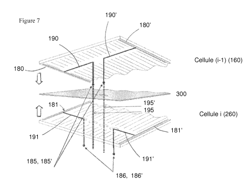
Wiring of the photovoltaic cells:
The architecture of the electrical wiring of the
photovoltaic cells characterizes the invention. Reference
is made to figures 7-12. In figure 7, current-collecting
buses (180, 180', 181, 181') are placed laterally at either
end of a cell i by monolithic integration in series so as
to allow electrons generated by this photovoltaic cell to
be collected. The collecting buses extend over the side
edges of the substrate. To place these side collecting
buses, it is possible to use automatic soldering machines
or even to make the connections manually.
Two connecting strips (190, 190', 191, 191') are then
connected to each collecting bus. Each connecting strip
serves as a link between the two electrical collecting
buses and contact zones external to the module. The
connecting strips lie perpendicular to the direction of the
current-collecting buses and are each brought toward the
center of the substrate. The length of the portion of the
connecting strip lying perpendicular to the direction of
the current-collecting buses varies in the photovoltaic
cells shown in the diagram of figure 7. Specifically, it
will be noted in figure 7 that the portion of the
connecting strips (191, 191') fixed to the photovoltaic
cell (i) is shorter than the portion of the connecting
strips (190, 190') fixed to the photovoltaic cell (i-1).
This length variation allows the position of the current
CA 02767550 2012-01-06
output terminals (185, 185', 186 and 186') to be shifted.
This shift makes it possible to ensure that the current
output terminals of the photovoltaic cells are not aligned
on top of one another, which would make subsequent
5 connection of the current output terminals to a junction
box difficult and which could cause short-circuits between
these terminals. It is possible to extend the connecting
strips (190, 190') of the cell i-1 so that said strips pass
through all the cells ranging from cell i to cell n and the
10 encapsulants and protrude from the back face of the
photovoltaic cell. The connecting-strip extension pieces
are given the references 195 and 195' in figure 7. Figure 8
shows the multielectrode photovoltaic device once
assembled.
15 Figure 9 shows, for a stack of four photovoltaic
cells, that the length of the connecting strip
perpendicular to the direction of the current-collecting
buses gets smaller from the front photovoltaic cell to the
back photovoltaic cell. The lengths of the connecting
20 strips lying perpendicular to the direction of the current-
collecting buses are identical for the two electrodes of a
given photovoltaic cell.
It is necessary to electrically isolate the two
connecting strips of the electrode located on face A of the
substrate. To do this, a strip of insulating material is
placed between face A and the two connecting strips.
According to a preferred embodiment, the current
output terminals protrude from the substrate and lie in a
plane parallel to the substrate. This is known as an "edge
face electrode" configuration (figures 10a and 10b). The
current output terminals of the cell i are extended so that
they protrude from the edge face (or side face) of the
substrates and encapsulant. The device consisting of the
stack of photovoltaic cells has a parallelepiped shape
comprising an upper face, a lower face and four side faces.
The upper face is the face that receives the light. The
"edge face electrode" configuration corresponds to the
current output terminals exiting from one of the side faces
CA 02767550 2012-01-06
21
of the photovoltaic device. After assembly of the various
elements of the photovoltaic device, it will be noted that
the current output terminals (185, 186, 187, 188, 185',
186', 187' and 188') are shifted relative to one another.
The expression "shifted current output terminals" is
understood to mean that no two current output terminals are
located in a given plane perpendicular to the plane formed
by the upper face of the photovoltaic device.
In a different embodiment in which the connection is
still made to the edge face (or side face) of the
photovoltaic device, it is possible to provide plugs (400,
400') that cooperate with contacts (500, 500') located on
the ends of the connecting strips (figures 13a and 13b).
The contacts may be located either on the edge face (or
side face) of the photovoltaic cell, or in a housing (600,
600') located on the edge face (or side face) of the
photovoltaic cell.
It is also possible to envision an embodiment such as
shown in figures 10c, 10d and 10e, in which the connecting-
strip lengths lying perpendicular to the direction of the
current-collecting buses are different for the two
electrodes of a given photovoltaic cell.
According to another preferred embodiment, the current
output terminals protrude from the substrate and lie in a
plane perpendicular to the substrate. This is known as a
"back face electrode" configuration (figures lla, lib and
llc). The "back face electrode" configuration therefore
corresponds to the current output terminals exiting from
the lower face of the photovoltaic device.
In the case of production of a multijunction and
multielectrode photovoltaic cell in which the electrodes
are located on the edge face (or side face) of the cell, it
is not necessary for the substrates to have been drilled
beforehand.
In the case of production of a multijunction and
multielectrode photovoltaic cell in which the electrodes
are located on the back face of the cell, it is necessary
for the substrate to have been prepared beforehand. This is
CA 02767550 2012-01-06
22
because, in order to allow the electrodes of each
photovoltaic cell with two independent electrodes to reach
the back face of the module, the substrates i=2 to n must
be drilled with apertures to allow the current output
terminals to pass (figure lla). The cell 2 comprises 4
apertures (350, 351, 352, 353). The cell 3 comprises 6
apertures (360, 361, 362, 363). The back cell comprises 8
apertures (370, 371, 372, 373, 374, 375, 376, 377). For a
given cell, the presence of 2 apertures each located at the
ends of the set of apertures is optional. This is because,
these two apertures may be absent provided that the
connecting strips are placed on the lower face of the
photovoltaic cell. However, their presence is necessary if
the connecting strips are placed on the upper face of the
photovoltaic cell. The substrate of the front cell (i=l)
has no drilled aperture. This is because the front cell
serves as a cover for the final multielectrode photovoltaic
cell. In addition, the internal ends of the connecting
strips of the cell i coincide with apertures present in the
encapsulant i (figure lla). It is possible to extend the
connecting strips of the cell i so that the connecting
strip passes through all of the substrates and encapsulants
and protrudes from the back face of the multielectrode
photovoltaic cell, as was described with regard to figure
7.
It is important, when using extension pieces to extend
the connecting strips (195, 195'), to ensure that these
extension pieces exit from face S of the substrate. In this
case, when the intermediate two-electrode photovoltaic cell
i (1<i<n) is placed in the stack so that face E corresponds
to face A and face S corresponds to face B, it is necessary
to ensure that the extension pieces of the connecting
strips of the photovoltaic cell i pass through apertures
drilled in the substrate i and provided for this purpose
(figure 12a).
When the intermediate two-electrode photovoltaic cell
i (1<i<n) is placed in the stack so that face E corresponds
to face B and face S to face A, the extension pieces of the
CA 02767550 2012-01-06
23
connecting strips of the photovoltaic cell i do not pass
through the apertures in the substrate i (figure 12b).
When the intermediate two-electrode photovoltaic cell
i (1<i<n) is placed in the stack so that face E corresponds
to face B and face S corresponds to face A, the substrate i
supporting the photovoltaic cell i will comprise 2i
apertures drilled beforehand in a line parallel to one of
the edges of the substrate. For this substrate, the 2(i-1)
central apertures coincide with the apertures drilled in
the interlayer (i-1). The substrate may comprise two
additional apertures on either side of these apertures.
When the intermediate two-electrode photovoltaic cell
i (1<i<n) is placed in the stack so that face E corresponds
to face A and face S corresponds to face B, the substrate i
supporting the photovoltaic cell i will comprise 2(i-1)
apertures drilled in a line parallel to one of the edges of
the substrate. For this substrate, the 2(i-1) central
apertures coincide with the apertures drilled in the
interlayer i.
The substrate of the back cell (i=n) will comprise 2n
apertures drilled in a line parallel to one of the edges of
the substrate. For this substrate, the 2(n-1) central
apertures correspond to the apertures drilled in the
interlayer (n-1). The substrate may also comprise two
additional apertures on either side of these apertures.
So as not to reduce the overall conversion efficiency
of the final multielectrode photovoltaic module, it is
preferable to locate the collecting buses and current
output terminals of each of the cells in the same place.
It is possible not to use connecting-strip extension
pieces. The electrical connection between each photovoltaic
cell and the junction box is then made possible by virtue
of plugs (400, 400') of different lengths which cooperate
with contacts (500, 500') placed on the back face of the
photovoltaic cell (figures 14a and 14b).
The placement and soldering of the various collecting
buses and connecting strips may be carried out manually.
However, typically this operation is carried out using an
CA 02767550 2012-01-06
24
automatic system. The electrical collecting buses and the
current output terminals may be metal strips such as silver
ribbons covered with nickel, nickel ribbons covered with
silver, tin beads, copper ribbons covered with tin, tin
ribbons covered with copper or any other material which
allows the current generated by the photovoltaic cell to be
transported and which can be soldered to the electrodes of
the photovoltaic cell.
Choice of the lamination interlayers:
Once each of the front, intermediate and back
photovoltaic cells has been independently manufactured they
are joined to one another via an (encapsulant) lamination
interlayer.
The lamination interlayer chosen to join the two-
electrode cells into a multijunction and multielectrode
cell should:
- provide mechanical protection,
- act as a barrier to water vapor and oxygen,
- provide electrical isolation,
- act as a shock absorber,
- not be a source of corrosion of the materials of the
cell,
- have adhesive properties.
The choice may for example be made from elastomers
such as for example ethylene/vinyl acetate (EVA),
polyurethane resins (PUR), polyacrylate resins or silicones
and thermoplastics such as polyvinyl butyral (PVB),
polyurethane thermoplastics (PUTs) and certain modified
polyolefins (EPDM, DMP), for example. Other lamination
interlayers may be used with the EVA or instead of the
latter, for example a plastic of the Tedlar , Nuvasil or
Tefzel type, or UV-setting coatings and combinations of
the above.
The lamination interlayer is as transparent as
possible and is highly transmissive to solar radiation in
the wavelength range corresponding to the absorption
spectrum of the materials forming the absorbing material of
the photovoltaic cell i and of all of the following
CA 02767550 2012-01-06
photovoltaic cells (from i+l to n), so as not to reduce the
efficiency of the photovoltaic module.
Preparation of the encapsulants:
All the encapsulants are the same size as the
5 substrates.
When a multijunction and multielectrode photovoltaic
cell is produced the electrodes of which are located on the
edge face (or side face) of the cell, it is not necessary
for the encapsulants to be prepared in advance (figures l0a
10 and b).
When a multijunction and multielectrode photovoltaic
cell is produced the electrodes of which are located on the
back face of the cell, it is necessary for the encapsulants
to be prepared beforehand. This is because, in order for
15 the electrodes of each photovoltaic cell with two
independent electrodes to reach the back face of the
module, the encapsulants i=1 to (n-1) are drilled with
apertures (figure lla, llb, llc).
Generally, the encapsulant i located between the
20 substrate of the cell i and the substrate of the cell (i+l)
will comprise 2i apertures drilled beforehand in a line
parallel to one of the edges of the substrate. For this
substrate, the 2(i-1) central apertures are coincident with
the apertures drilled in the substrate i.
25 A seal or sealing resin will also possibly be placed
between each substrate, either on the periphery of face S
of the substrate i, or on the periphery of face E of the
substrate (i+l), so as to provide an additional seal
between substrates i and (i+l), especially with regard to
moisture. This seal or sealing resin may for example be a
hot-melt polymer such as ethylene/vinyl acetate or
polyisobutylene or a mastic for example based on
polyurethane, polysulfide or silicone.
Solder joints in apertures of the back substrate may
then also be covered with epoxide, for example, with a view
to providing additional protection with regard to the
environment.
CA 02767550 2012-01-06
26
Assembly of the multijunction and multielectrode
photovoltaic cell from independent two-electrode
photovoltaic cells and lamination interlayers:
The various two-electrode photovoltaic cells are
joined to one another. To do this, the lamination
interlayer 1 is placed on the surface of face S of the
photovoltaic cell 1. Face E of the cell 2 is then placed on
the lamination interlayer 1. Generally, to join
photovoltaic cells, the lamination interlayer i is
deposited on the surface of face S of the photovoltaic cell
i. Lastly, face E of the photovoltaic cell n is placed on
the surface of the lamination interlayer (n-1).
During this step of joining the various two-electrode
photovoltaic cells, when a multijunction and multielectrode
photovoltaic cell is to be produced the electrodes of which
are located on the back face of the cell, it is necessary
when placing the lamination interlayer i, to ensure that
the apertures provided in the lamination interlayer i
coincide with the internal ends of the connecting strips of
the i preceding cells. Likewise, when placing the cell i,
it is important to ensure that the apertures of the
interlayer (i-1) coincide with the apertures of the
substrate i.
When a multielectrode cell the electrodes of which are
located on the back face of the cell makes use of
connecting-strip extension pieces it is necessary to ensure
that the extension pieces of the connecting strips of the
i-1 preceding cells pass through coincident apertures in
the lamination interlayer i and to pass the two extension
pieces of the connecting strips of the photovoltaic cell i
through two free apertures in the lamination interlayer i.
Likewise, when placing the cell i, it is important to
ensure that the apertures of the interlayer (i-1) coincide
with the apertures of the substrate i (figure lla).
In the case where contact is made to a multielectrode
cell via the edge face (or side face) of the cell, it is
important to ensure that the connecting strips of the two
electrodes of the photovoltaic cell i, which are located on
CA 02767550 2012-01-06
27
the edge face (or side face) of the substrate i, are not
placed exactly above the connecting strips of the
electrodes of the preceding (i-1) photovoltaic cells
(figure 10b).
During this step of joining the various parts of the
multijunction and multielectrode photovoltaic cell, it is
necessary to ensure, in each step, that the substrates and
lamination interlayers are well aligned with one another.
This alignment may be carried out manually by operators or
automatically using an image control, for example, and the
use of robots enabling alignment.
The array comprising the stack of n two-electrode
photovoltaic cells and the (n-1) interlayers is then placed
in a laminating system which allows joining of the
multijunction and multielectrode photovoltaic cell to be
completed. This final lamination may for example be carried
out in a vacuum laminator or in a roller laminator followed
by processing in an autoclave.
The photovoltaic-cell module obtained in this way may
be connected to one or more junction boxes via current
output terminals that are all located on the same side of
the module or on its edge face. The junction box ensures
electrical connection of the module to a user interface,
generally consisting of an electronic device allowing a DC
voltage to be converted into an AC voltage compatible with
the mains grid. Preferably, the module is connected to a
single junction box. Preferably the single junction box is
installed in the frame of the panel serving to support the
photovoltaic-cell module for modules with side face
electrodes and on the face S of the back cell for modules
with back face electrodes.