Note: Descriptions are shown in the official language in which they were submitted.
CA 02767776 2014-04-29
ELECTRONIC DEVICES WITH CAPACITIVE PROXIMITY SENSORS FOR
PROXIMITY-BASED RADIO-FREQUENCY POWER CONTROL
This application claims priority to United States
provisional patent application No. 61/226,683, filed July
17, 2009, and United States patent application No.
12/632,695, filed December 7, 2009.
Background
This relates generally to antennas, and, more
particularly, to antennas for electronic devices.
Electronic devices such as portable computers and
handheld electronic devices are becoming increasingly
popular. Devices such as these are often provided with
wireless communications capabilities. For example,
electronic devices may use long-range wireless
communications circuitry such as cellular telephone
1
CA 02767776 2012-01-10
WO 2011/008434
PCT/US2010/039492
circuitry to communicate using cellular telephone bands at
850 MHz, 900 MHz, 1800 MHz, and 1900 MHz (e.g., the main
Global System for Mobile Communications or GSM cellular
telephone bands). Long-range wireless communications
circuitry may also be used handle the 2100 MHz band and
other bands. Electronic devices may use short-range
wireless communications links to handle communications
with nearby equipment. For example, electronic devices
may communicate using the WiFi0 (IEEE 802.11) bands at 2.4
GHz and 5 GHz (sometimes referred to as local area network
bands) and the Bluetooth0 band at 2.4 GHz.
It can be difficult to incorporate antennas
successfully into an electronic device. Some electronic
devices are manufactured with small form factors, so space
for antennas is limited. In many electronic devices, the
presence of electronic components in the vicinity of an
antenna serves as a possible source of electromagnetic
interference. Antenna operation can also be blocked by
conductive structures. This can make it difficult to
implement an antenna in an electronic device that contains
conductive housing walls or other conductive structures
that can potentially block radio-frequency signals.
Radio-frequency transmit power limits may be imposed by
regulatory bodies. These limits pose challenges when
operating an electronic device antenna at elevated power
levels.
It would therefore be desirable to be able to
provide improved antennas for wireless electronic devices.
Summary
An electronic device such as a tablet computer
or other portable device may have a conductive housing. A
portion of the conductive housing in each device may serve
as antenna ground for an antenna. The antenna may be fed
2
CA 02767776 2014-04-29
using a positive antenna feed terminal coupled to an
antenna resonating element and a ground antenna feed
terminal coupled to the conductive housing.
The antenna resonating element may be mounted
adjacent to an antenna window in the conductive housing. To
ensure that desired maximum output power limits for radio-
frequency signals are satisfied when an external object
such as a human body is in the vicinity of the antenna
window, the electronic device may be provided with a
capacitive proximity sensor. The proximity sensor may have
a capacitive proximity sensor electrode that is interposed
between the antenna resonating element and the antenna
window. During operation, the proximity sensor may detect
when an external object such as part of a user's body comes
within a given distance of the proximity sensor and the
antenna. When these conditions are detected, circuitry in
the electronic device may reduce the maximum transmitted
output power through the antenna.
The capacitive proximity sensor electrode may
have first and second conductive layers that are separated
by a dielectric layer. First and second inductors may be
used to couple the first and second conductive layers to
respective first and second inputs of a signal detector
such as a capacitance-to-digital converter.
The capacitive proximity sensor electrode may
serve as a parasitic antenna resonating element for the
antenna that helps to reduce radio-frequency signal
hotspots. A capacitor may be used to connect the capacitive
proximity sensor electrode to the conductive housing.
Accordingly, in a further aspect, the present
invention provides an electronic device, comprising: a
housing; an antenna window in the housing; an antenna
3
CA 02767776 2014-04-29
resonating element mounted in the housing so that radio-
frequency signals are transmitted through the antenna
window; a capacitive proximity sensor electrode located
between the antenna resonating element and the antenna
window; a capacitance-to-digital converter having first and
second inputs; and first and second radio-frequency choke
inductors coupled between the capacitive proximity sensor
electrode and the capacitance-to-digital converter.
In a further aspect, the present invention provides a
tablet computer comprising: a conductive housing; a
dielectric antenna window in the conductive housing; radio-
frequency transceiver circuitry; an antenna with which the
radio-frequency transceiver circuitry transmits radio-
frequency signals in at least one cellular telephone band,
wherein the antenna comprises an antenna ground formed from
at least portion of the conductive housing and an antenna
resonating element mounted adjacent to the dielectric
antenna window; a capacitive proximity sensor electrode
mounted between the antenna resonating element and the
dielectric antenna window; and a capacitance-to-digital
converter coupled to the capacitive proximity sensor
electrode.
In a still further aspect, the present invention
provides an electronic device comprising: at least one
conductive housing structure to which a ground antenna feed
terminal is connected; an antenna window in the housing
structure; an antenna resonating element formed from
conductive traces on a flex circuit to which a positive
antenna feed terminal is connected; radio-frequency
transceiver circuitry that is coupled to the positive
antenna feed terminal and the ground antenna feed terminal
and that transmits radio-frequency signals through the
3a
CA 02767776 2014-04-29
antenna window using the antenna resonating element; a
capacitive proximity sensor electrode interposed between
the antenna resonating element and the antenna window,
wherein the radio-frequency transceiver circuitry transmits
the radio-frequency signals at an output power; and
circuitry coupled to the capacitive proximity sensor
electrode that limits the output power when an external
object is detected within a given distance of the
capacitive proximity sensor electrode.
Further features of the invention, its nature and
various advantages will be more apparent from the
accompanying drawings and the following detailed
description of the preferred embodiments.
3b
CA 02767776 2012-01-10
WO 2011/008434
PCT/US2010/039492
Brief Description of the Drawings
FIG. 1 is a front perspective view of an
illustrative electronic device with an antenna and
proximity sensor in accordance with an embodiment of the
present invention.
FIG. 2 is a rear perspective view of an
illustrative electronic device with an antenna and
proximity sensor in accordance with an embodiment of the
present invention.
FIG. 3 is a schematic diagram of an illustrative
electronic device with antenna and proximity sensor
structures in accordance with an embodiment of the present
invention.
FIG. 4 is a cross-sectional side view of an
illustrative electronic device with an antenna and
proximity sensor in accordance with an embodiment of the
present invention.
FIG. 5 is a diagram of an illustrative
electronic device having an antenna and wireless circuitry
that may reduce the amount of power transmitted through
the antenna when a proximity sensor detects that an
external object is within a given range of the antenna and
the electronic device in accordance with an embodiment of
the present invention.
FIG. 6 is a perspective view of an illustrative
antenna having an antenna resonating element and a
proximity sensor electrode serving as a parasitic antenna
resonating element that overlap a dielectric antenna
window in accordance with an embodiment of the present
invention.
FIG. 7 is a graph showing how the presence of a
parasitic antenna resonating element may help to reduce
radio-frequency signal hotspots and thereby reduce near
4
CA 02767776 2012-01-10
WO 2011/008434
PCT/US2010/039492
field radiation hotspots produced by an antenna in an
electronic device in accordance with an embodiment of the
present invention.
FIG. 8 is a top view of a parasitic antenna
resonating element such as a capacitive proximity sensor
electrode that has been coupled by a capacitor to a
portion of a conductive device housing that is serving as
antenna ground in accordance with an embodiment of the
present invention.
FIG. 9 is a diagram showing how a proximity
sensor may have a capacitor electrode for detecting the
presence of external objects such as a part of a user's
body in accordance with an embodiment of the present
invention.
FIG. 10 is a diagram showing how a capacitive
proximity sensor may have a two-layer capacitive sensor
having a shield electrode and a sensor electrode that are
monitored by a capacitance-to-digital converter in
accordance with an embodiment of the present invention.
FIG. 11 is a perspective view of an illustrative
two-layer capacitive proximity sensor electrode structure
in accordance with an embodiment of the present invention.
FIG. 12 is a perspective view of an elongated
two-layer capacitive proximity sensor electrode in
accordance with an embodiment of the present invention.
Detailed Description
Electronic devices may be provided with wireless
communications circuitry. The wireless communications
circuitry may be used to support wireless communications
in one or more wireless communications bands. For
example, the wireless communications circuitry may
transmit and receive signals in cellular telephone bands.
To satisfy consumer demand for small form factor
5
CA 02767776 2012-01-10
WO 2011/008434
PCT/US2010/039492
wireless devices, manufacturers are continually striving
to reduce the size of components that are used in these
devices while providing enhanced functionality.
Particularly in configurations in which an electronic
device is used in transmitting and receiving radio-
frequency signals in cellular telephone bands and other
communications bands that have relatively wide bandwidths,
it can be challenging to meet desired antenna performance
criteria in a compact device. High transmit powers and
wide antenna bandwidths can be desirable to ensure
adequate signal strength during communications, but these
attributes may give rise to challenges with controlling
emitted radiation levels.
It is generally impractical to completely shield
a user of an electronic device from transmitted radio-
frequency signals. For example, conventional cellular
telephone handsets generally emit signals in the vicinity
of a user's head during telephone calls. Government
regulations limit radio-frequency signal powers. At the
same time, wireless carriers require that the user
equipment that is used in their networks be capable of
producing certain minimum radio-frequency powers so as to
ensure satisfactory operation of the equipment.
In many jurisdictions, specific absorption rate
(SAR) standards are in place that impose maximum energy
absorption limits on handset manufacturers. These
standards place restrictions on the amount of radiation
that may be emitted at any particular point within a given
distance of the antenna. Particular attention is given to
radiation limits at distances of about 1-20 mm from the
device, where users are likely to place a body part near
an antenna.
Satisfactory antenna performance and regulatory
compliance can be ensured by using an antenna does not
6
CA 02767776 2012-01-10
WO 2011/008434
PCT/US2010/039492
exhibit local "hotspots" in which emitted radiation
exceeds desired power levels. A proximity sensor may also
be used to detect when an external object such as a user's
body is in the vicinity of the antenna. When the presence
of the external object is detected, transmitted power
levels can be reduced.
Hotspots can be minimized by proper antenna
design. If desired, a parasitic antenna resonating
element may be placed in the vicinity of a device antenna
to help smooth out near-field emitted radiation patterns.
Electromagnetic shielding arrangements may also be
implemented using ferrite tape or other high permeability
materials.
Any suitable electronic devices may be provided
with antennas and proximity sensors that use these
configurations. As an example, antennas and proximity
sensors may be formed in electronic devices such as
desktop computers, portable computers such as laptop
computers and tablet computers, handheld electronic
devices such as cellular telephones, etc. With one
suitable configuration, which is sometimes described
herein as an example, the antennas and proximity sensors
are formed in relatively compact electronic devices in
which interior space can be valuable. These compact
devices may be portable electronic devices.
Portable electronic devices that may be provided
with antennas and proximity sensors include laptop
computers and small portable computers such as
ultraportable computers, netbook computers, and tablet
computers. Portable electronic devices may also be
somewhat smaller devices. Examples of smaller portable
electronic devices that may be provided with antennas
include cellular telephones, wrist-watch devices, pendant
devices, headphone and earpiece devices, and other
7
CA 02767776 2012-01-10
WO 2011/008434
PCT/US2010/039492
wearable and miniature devices.
Space is at a premium in portable electronic
devices and housings for these devices are sometimes
constructed from conductive materials that block antenna
signals. Arrangements in which antenna structures and
proximity sensors are formed behind an antenna window can
help address these challenges. Antenna windows may be
formed in conductive housing walls by forming a dielectric
antenna window structure from an opening in the conductive
housing wall. If desired, slot-based antenna windows may
be formed in conductive housing walls. In a slot-based
antenna window, the window region is defined by a pattern
of window slots. Arrangements in which dielectric antenna
windows are used are sometimes described herein as an
example.
An antenna resonating element may be formed
under the antenna window. Portions of the conductive
housing or other conductive structures may serve as
antenna ground. The antenna can be fed using a positive
antenna feed terminal that is coupled to the antenna
resonating element and using a ground antenna feed
terminal that is coupled to the conductive housing.
During operation, radio-frequency signals for the antenna
can pass through the antenna window. The parasitic
antenna resonating element and ferrite tape may help to
reduce near-field hotspots.
A proximity-based antenna power control circuit
may be used to reduce near-field electromagnetic radiation
intensities when the presence of an external object is
detected in the vicinity of the antenna. The proximity-
based antenna power control circuit may be based on a
capacitive proximity sensor. Sensor electrodes for the
capacitive proximity sensor may be placed in the vicinity
of the antenna. If desired, a conductive structure such
8
CA 02767776 2012-01-10
WO 2011/008434
PCT/US2010/039492
as a sensor electrode may serve both as part of a
capacitive sensor and as part of a parasitic antenna
resonating element. With this type of arrangement, the
sensor electrode may be used in reducing near-field
radiation hotspots while simultaneously serving as part of
a capacitor electrode that detects the presence of nearby
external objects for a proximity detector.
Antenna and proximity sensor structures with
configurations such as these can be mounted on any
suitable exposed portion of a portable electronic device.
For example, antennas and proximity sensors can be
provided on the front or top surface of the device. In a
tablet computer, cellular telephone, or other device in
which the front of the device is all or mostly occupied
with conductive structures such as a touch screen display,
it may be desirable to form at least part of an antenna
window on a rear device surface. Other configurations are
also possible (e.g., with antennas and proximity sensors
mounted in more confined locations, on device sidewalls,
etc.). The use of antenna mounting locations in which at
least part of a dielectric antenna window is formed in a
conductive rear housing surface is sometimes described
herein as an example, but, in general, any suitable
antenna mounting location may be used in an electronic
device if desired.
An illustrative portable device that may include
an antenna and proximity sensor is shown in FIG. 1. As
shown in FIG. 1, device 10 may be a relatively thin device
such as a tablet computer. Device 10 may have display
such as display 50 mounted on its front (top) surface.
Housing 12 may have curved portions that form the edges of
device 10 and a relatively planar portion that forms the
rear surface of device 10 (as an example). An antenna
window such as antenna window 58 may be formed in housing
9
CA 02767776 2012-01-10
WO 2011/008434
PCT/US2010/039492
12. Antenna structures for device 10 may be formed in the
vicinity of antenna window 58.
Device 10 may have user input-output devices
such as button 59. Display 50 may be a touch screen
display that is used in gathering user touch input. The
surface of display 50 may be covered using a dielectric
member such as a planar cover glass member. The central
portion of display 50 (shown as region 56 in FIG. 1) may
be an active region that is sensitive to touch input. The
peripheral regions of display 50 such as regions 54 may be
inactive regions that are free from touch sensor
electrodes. A layer of material such as an opaque ink may
be placed on the underside of display 50 in peripheral
regions 54 (e.g., on the underside of the cover glass).
This layer may be transparent to radio-frequency signals.
The conductive touch sensor electrodes in region 56 may
tend to block radio-frequency signals. However, radio-
frequency signals may pass through the cover glass and
opaque ink in inactive display regions 54 (as an example).
In the opposite direction, radio-frequency signals may
pass through antenna window 58. Lower-frequency
electromagnetic fields also pass through window 58, so
capacitance measurements for a proximity sensor may be
made through antenna window 58.
Housing 12 may be formed from one or more
structures. For example, housing 12 may include an
internal frame and planar housing walls that are mounted
to the frame. Housing 12 may also be formed from a
unitary block of material such as a cast or machined block
of aluminum. Arrangements that use both of these
approaches may also be used if desired.
Housing 12 may be formed of any suitable
materials including plastic, wood, glass, ceramics, metal,
or other suitable materials, or a combination of these
CA 02767776 2012-01-10
WO 2011/008434
PCT/US2010/039492
materials. In some situations, portions of housing 12 may
be formed from a dielectric or other low-conductivity
material, so as not to disturb the operation of conductive
antenna elements that are located in proximity to housing
12. In other situations, housing 12 may be formed from
metal elements. An advantage of forming housing 12 from
metal or other structurally sound conductive materials is
that this may improve device aesthetics and may help
improve durability and portability.
With one suitable arrangement, housing 12 may be
formed from a metal such as aluminum. Portions of housing
12 in the vicinity of antenna window 58 may be used as
antenna ground. Antenna window 58 may be formed from a
dielectric material such as polycarbonate (PC),
acrylonitrile butadiene styrene (ABS), a PC/ABS blend, or
other plastics (as examples). Window 58 may be attached
to housing 12 using adhesive, fasteners, or other suitable
attachment mechanisms. To ensure that device 10 has an
attractive appearance, it may be desirable to form window
58 so that the exterior surfaces of window 58 conform to
the edge profile exhibited by housing 12 in other portions
of device 10. For example, if housing 12 has straight
edges 12A and a flat bottom surface, window 58 may be
formed with a right-angle bend and vertical sidewalls. If
housing 12 has curved edges 12A, window 58 may have a
similarly curved surface.
FIG. 2 is a rear perspective view of device 10
of FIG. 1 showing how device 10 may have a relatively
planar rear surface 12B and showing how antenna window 58
may be rectangular in shape with curved portions that
match the shape of curved housing edges 12A.
A schematic diagram of device 10 showing how
device 10 may include one or more antennas 26 and
transceiver circuits that communicate with antennas 26 is
11
CA 02767776 2012-01-10
WO 2011/008434
PCT/US2010/039492
shown in FIG. 3. Electronic device 10 of FIG. 3 may be a
portable computer such as a laptop computer, a portable
tablet computer, a mobile telephone, a mobile telephone
with media player capabilities, a handheld computer, a
remote control, a game player, a global positioning system
(GPS) device, a desktop computer, a combination of such
devices, or any other suitable electronic device.
As shown in FIG. 3, electronic device 10 may
include storage and processing circuitry 16. Storage and
processing circuitry 16 may include one or more different
types of storage such as hard disk drive storage,
nonvolatile memory (e.g., flash memory or other
electrically-programmable-read-only memory), volatile
memory (e.g., static or dynamic random-access-memory),
etc. Processing circuitry in storage and processing
circuitry 16 may be used to control the operation of
device 10. Processing circuitry 16 may be based on a
processor such as a microprocessor and other suitable
integrated circuits. With one suitable arrangement,
storage and processing circuitry 16 may be used to run
software on device 10, such as internet browsing
applications, voice-over-internet-protocol (VOIP)
telephone call applications, email applications, media
playback applications, operating system functions, control
functions for controlling radio-frequency power amplifiers
and other radio-frequency transceiver circuitry, etc.
Storage and processing circuitry 16 may be used in
implementing suitable communications protocols.
Communications protocols that may be implemented using
storage and processing circuitry 16 include internet
protocols, cellular telephone protocols, wireless local
area network protocols (e.g., IEEE 802.11 protocols --
sometimes referred to as WiFi0), protocols for other
short-range wireless communications links such as the
12
CA 02767776 2012-01-10
WO 2011/008434
PCT/US2010/039492
Bluetooth0 protocol, etc.
Input-output circuitry 14 may be used to allow
data to be supplied to device 10 and to allow data to be
provided from device 10 to external devices. Input-output
devices 18 such as touch screens and other user input
interface are examples of input-output circuitry 14.
Input-output devices 18 may also include user input-output
devices such as buttons, joysticks, click wheels,
scrolling wheels, touch pads, key pads, keyboards,
microphones, cameras, etc. A user can control the
operation of device 10 by supplying commands through such
user input devices. Display and audio devices may be
included in devices 18 such as liquid-crystal display
(LCD) screens, light-emitting diodes (LEDs), organic
light-emitting diodes (OLEDs), and other components that
present visual information and status data. Display and
audio components in input-output devices 18 may also
include audio equipment such as speakers and other devices
for creating sound. If desired, input-output devices 18
may contain audio-video interface equipment such as jacks
and other connectors for external headphones and monitors.
Wireless communications circuitry 20 may include
radio-frequency (RF) transceiver circuitry 23 formed from
one or more integrated circuits, power amplifier
circuitry, low-noise input amplifiers, passive RF
components, one or more antennas, and other circuitry for
handling RF wireless signals. Wireless signals can also
be sent using light (e.g., using infrared communications).
Wireless communications circuitry 20 may include
radio-frequency transceiver circuits for handling multiple
radio-frequency communications bands. For example,
circuitry 20 may include transceiver circuitry 22 that
handles 2.4 GHz and 5 GHz bands for WiFi (IEEE 802.11)
communications and the 2.4 GHz Bluetooth communications
13
CA 02767776 2012-01-10
WO 2011/008434
PCT/US2010/039492
band. Circuitry 20 may also include cellular telephone
transceiver circuitry 24 for handling wireless
communications in cellular telephone bands such as the GSM
bands at 850 MHz, 900 MHz, 1800 MHz, and 1900 MHz, and the
2100 MHz data band (as examples). Wireless communications
circuitry 20 can include circuitry for other short-range
and long-range wireless links if desired. For example,
wireless communications circuitry 20 may include global
positioning system (GPS) receiver equipment, wireless
circuitry for receiving radio and television signals,
paging circuits, etc. In WiFi and Bluetooth links and
other short-range wireless links, wireless signals are
typically used to convey data over tens or hundreds of
feet. In cellular telephone links and other long-range
links, wireless signals are typically used to convey data
over thousands of feet or miles.
Wireless communications circuitry 20 may include
antennas 26 such as the antenna located adjacent to
antenna window 58 of FIGS. 1 and 2. Antennas 26 may be
single band antennas that each cover a particular desired
communications band or may be multiband antennas. A
multiband antenna may be used, for example, to cover
multiple cellular telephone communications bands. If
desired, a dual band antenna may be used to cover two WiFi
bands (e.g., 2.4 GHz and 5 GHz). Different types of
antennas may be used for different bands and combinations
of bands. For example, it may be desirable to form a dual
band antenna for forming a local wireless link antenna, a
multiband antenna for handling cellular telephone
communications bands, and a single band antenna for
forming a global positioning system antenna (as examples).
Transmission line paths 44 may be used to convey
radio-frequency signals between transceivers 22 and 24 and
antennas 26. Radio-frequency transceivers such as radio-
14
CA 02767776 2012-01-10
WO 2011/008434
PCT/US2010/039492
frequency transceivers 22 and 24 may be implemented using
one or more integrated circuits and associated components
(e.g., switching circuits, matching network components
such as discrete inductors, capacitors, and resistors, and
integrated circuit filter networks, etc.). These devices
may be mounted on any suitable mounting structures. With
one suitable arrangement, transceiver integrated circuits
may be mounted on a printed circuit board. Paths 44 may
be used to interconnect the transceiver integrated
circuits and other components on the printed circuit board
with antenna structures in device 10. Paths 44 may
include any suitable conductive pathways over which radio-
frequency signals may be conveyed including transmission
line path structures such as coaxial cables, microstrip
transmission lines, etc.
Antennas 26 may, in general, be formed using any
suitable antenna types. Examples of suitable antenna
types for antennas 26 include antennas with resonating
elements that are formed from patch antenna structures,
inverted-F antenna structures, closed and open slot
antenna structures, loop antenna structures, monopoles,
dipoles, planar inverted-F antenna structures, hybrids of
these designs, etc. With one suitable arrangement, which
is sometimes described herein as an example, part of
housing 12 (e.g., the portion of housing 12 in the
vicinity of antenna window 58) may form a ground structure
for the antenna associated with window 58.
A cross-sectional view of device 10 in the
vicinity of antenna window 58 is shown in FIG. 4. As
shown in FIG. 4, antenna 26 may have antenna resonating
element 68 (e.g., a patch antenna resonating element, a
single arm inverted-F antenna structure, a dual-arm
inverted-F antenna structure, or other suitable multi-arm
or single arm inverted-F antenna structures, closed and
CA 02767776 2012-01-10
WO 2011/008434
PCT/US2010/039492
open slot antenna structures, loop antenna structures,
monopoles, dipoles, planar inverted-F antenna structures,
hybrids of these designs, etc. Housing 12 may serve as
antenna ground for antenna 26.
Antenna 26 may also have a parasitic antenna
resonating element formed from one or more conductive
structures such as structure 66. Structure 66 may
include, for example, a capacitive proximity sensor
electrode. If desired, a layer of ferrite material such
as ferrite tape 74 may be placed between antenna
resonating element 68 and window 58 to help reduce near-
field signal strengths without over-attenuating far-field
signals. In the example of FIG. 4, ferrite tape 74 has
been placed under structure 66.
As shown in FIG. 4, antenna 26 may be fed using
a positive antenna feed terminal that is coupled to
antenna resonating element 68 such as positive antenna
feed terminal 76 and a ground antenna feed terminal that
is coupled to housing 12 such as ground antenna feed
terminal 78.
Antenna resonating element 68 may be placed in
the vicinity of dielectric antenna window 58 as shown in
FIG. 4, so that radio-frequency signals can be conveyed
through window 58 (e.g., in directions 72 and 71). Radio-
frequency signals can also be conveyed through a
transparent display cover member such as cover glass 60.
Display 50 may have an active region such as region 56 in
which cover glass 60 has underlying conductive structure
such as display panel module 64. The structures in
display panel 64 such as touch sensor electrodes and
active display pixel circuitry may be conductive and may
therefore attenuate radio-frequency signals. In region
54, however, display 50 may be inactive (i.e., panel 64
may be absent). An opaque ink such as ink 62 may be
16
CA 02767776 2012-01-10
WO 2011/008434
PCT/US2010/039492
formed on the underside of transparent cover glass 60 in
region 54 to block antenna resonating element 68 from
view. Ink 62 and the dielectric material of cover member
60 in region 54 may be sufficiently transparent to radio-
frequency signals that radio-frequency signals can be
conveyed through these structures in directions 70.
Any suitable conductive materials may be used in
forming antenna structures for antenna 26. With one
suitable arrangement, the conductive structures for
antenna resonating element 68 and parasitic antenna
resonating element 66 may each be formed from conductive
traces on a dielectric support. The conductive traces may
be formed from copper or other metals (as an example) to
help ensure low losses and good performance at radio
frequencies. The dielectric supports for these structures
may be printed circuit boards or plastic members. Plastic
support structures may also be used to support printed
circuit boards. In general, printed circuit boards may be
rigid or flexible. Rigid printed circuit boards may be
formed from epoxy (e.g., FR4) or other dielectric
substrates. Flexible printed circuit boards ("flex
circuits") may be formed from flexible polymer sheets such
as polyimide sheets or other flexible dielectrics. When
an antenna structure is formed from a sheet of flex
circuit substrate, the flex circuit may, if desired, be
flexed to form a curved surface (e.g., to adapt to a
curved plastic support structure). With rigid substrate
arrangements, the printed circuit board is typically flat.
Structures such as conductive structure 66 may
serve multiple functions. For example, because structure
66 is adjacent to antenna resonating element 68, structure
66 influences the electromagnetic behavior of antenna 26
and can therefore serve as a parasitic antenna resonating
element. At the same time, conductive structure 66 may,
17
CA 02767776 2012-01-10
WO 2011/008434
PCT/US2010/039492
if desired, be used as a sensor electrode for a proximity
sensor.
Transceiver circuitry 23 may be mounted to
printed circuit board 79 and may be connected to the
conductive lines in transmission line 44 via connector 81
and traces in board 79. Transmission line 44 may have
positive and ground conductors and may be used in
conveying radio-frequency antenna signals between
transceiver 23 and feed terminals 76 and 78 of antenna 26.
Device 10 and antenna window 58 may have any
suitable dimensions. For example, device 10 may have
lateral dimensions of about 10-50 cm. Device 10 may be
more than 2 cm thick, less than 2 cm thick, less than 1.5
cm thick, or less than 0.5 cm thick.
In thin device configurations, the removal of
conductive housing portions in the immediate vicinity of
antenna resonating element 68 helps ensure that antenna 26
will exhibit satisfactory efficiency and bandwidth (e.g.,
for supporting communications in wide bandwidth long-range
communications bands such as cellular telephone
communications bands).
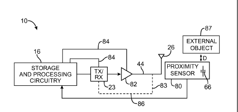
A circuit diagram showing how a proximity sensor
signal may be used in controlling the amount of power that
is transmitted by antenna 26 is shown in FIG. 5. As shown
in FIG. 5, device 10 may include storage and processing
circuitry 16 (see, e.g., FIG. 3). Device 10 may also
include a proximity sensor such as proximity sensor 80.
Proximity sensor 80 may be implemented using any suitable
type of proximity sensor technology (e.g., capacitive,
optical, etc.). An advantage of capacitive proximity
sensing techniques is that they can be relatively
insensitive to changes in the reflectivity of external
object 87.
As shown in the example of FIG. 5, proximity
18
CA 02767776 2012-01-10
WO 2011/008434
PCT/US2010/039492
sensor 80 may contain a capacitor electrode formed from a
conductive member such as conductive member 66 (FIG. 4).
Conductive member 66 may, if desired, serve as a parasitic
antenna resonating element for antenna 26.
Proximity sensor 80 may be mounted in housing 12
in the vicinity of antenna 26 (as shown in FIG. 4) to
ensure that the signal from proximity sensor 80 is
representative of the presence of external object 87 in
the vicinity of antenna 26 (e.g., within a distance D of
antenna 26 and/or device 10).
Output signals from proximity sensor 80 may be
conveyed to storage and processing circuitry 16 using path
86. The signals from proximity sensor 80 may be analog or
digital signals that provide proximity data to storage and
processing circuitry 16. The proximity data may be
Boolean data indicating that object 87 is or is not within
a given predetermined distance of antenna 26 or may be
continuous data representing a current estimated distance
value for D.
Storage and processing circuitry 16 may be
coupled to transceiver circuitry 23 and power amplifier
circuitry 82. Dashed line 83 shows how received radio-
frequency signals can be conveyed from antenna 26 to
transceiver circuitry 23. During data transmission
operations, control lines 84 may be used to convey control
signals from storage and processing circuitry 16 to
transceiver circuitry 23 and power amplifier circuitry 82
to adjust output powers in real time. For example, when
data is being transmitted, transceiver 23 and is
associated output amplifier 82 can be directed to increase
or decrease the power level of the radio-frequency signal
that is being provided to antenna 26 over transmission
line 44 to ensure that regulatory limits for
electromagnetic radiation emission are satisfied. If, for
19
CA 02767776 2012-01-10
WO 2011/008434
PCT/US2010/039492
example, proximity sensor 80 does not detect the presence
of external object 87, power can be provided at a
relatively high (unrestricted) level. If, however,
proximity sensor 80 determines that the user's leg or
other body part or other external object 87 is in the
immediate vicinity of antenna 26 (e.g., within 20 mm or
less, within 15 mm or less, within 10 mm or less, etc.),
storage and processing circuitry can respond accordingly
by directing transceiver circuitry 23 and/or power
amplifier 82 to transmit radio-frequency signals through
antenna 26 at reduced powers.
A perspective view of an illustrative antenna 26
is shown in FIG. 6. As shown in FIG. 6, antenna
resonating element 68 may contain one or more conductive
traces such as conductive trace 96. In the example of
FIG. 6, antenna resonating element 68 has an inverted-F
configuration. With this configuration, antenna
resonating element 68 may have a dielectric substrate such
as rigid or flexible printed circuit substrate 90 on which
a conductive pattern has been formed such as conductive
trace 94. Conductive trace 94 may have a main resonating
element arm 92, a short circuit branch such as branch 96
that shorts arm 92 to ground (e.g., a path coupled to
antenna feed terminal 78 of FIG. 4), and a branch 98 to
which positive antenna feed terminal 76 is coupled. Arm
92 may, if desired, be provided with different shapes
(e.g., multiple branches) to support operation in desired
communications bands with desired bandwidths. The trace
pattern for antenna resonating element 68 that is shown in
FIG. 6 is merely illustrative. In general, any suitable
type of antenna resonating element pattern may be used for
antenna resonating element 68 if desired.
Antenna resonating element 68 may be mounted so
as to overlap antenna window 58 and so as to lie under
CA 02767776 2012-01-10
WO 2011/008434
PCT/US2010/039492
inactive region 54 of display 50 (FIG. 4). Conductive
structure 66 may be interposed between antenna resonating
element 68 and window 58.
During operation of antenna 26, the
electromagnetic fields that are produced by antenna
resonating element 68 may induce currents in conductive
housing 12, such as currents 95 in the vicinity of window
58. If care is not taken, the relative shapes and sizes
of the components of antenna 26 may give rise to
undesirable concentrations of currents. This can, in
turn, lead to undesirable hotspots in the near-field
radiation pattern for antenna 26, as the induced currents
re-radiate electromagnetic energy through antenna window
58.
A graph that illustrates how antenna signals may
exhibit undesirable hotspots is shown in FIG. 7. In the
graph of FIG. 7, the power associated with near-field
transmitted radio-frequency signals (e.g., signals for an
antenna 26 that have been emitted in direction 72 or 71
through antenna window 58) is shown as a function of
position (e.g., position along the inner edge of antenna
window 58). Solid line 120 corresponds to a possible
near-field radiation pattern in the absence of suitable
antenna structures to reduce hotspots in currents 95 and
associated hotspots in emitted radio-frequency signal
powers. Dashed line 122 shows how hotspots can minimized
or eliminated by inclusion of proper hotspot-reducing
structures. Because dashed line 122 is smoother than line
120 and exhibits lower peak powers, dashed line 122
reflects a reduced spatial concentration of radio-
frequency signal power. Smoothed radiation
characteristics help antenna 26 to transmit desired
amounts of signal power when communicating with a remote
base station without exceeding regulatory limits for
21
CA 02767776 2012-01-10
WO 2011/008434
PCT/US2010/039492
emitted radiation levels.
The near-field radiation pattern smoothing
structures may include structures such as parasitic
antenna resonating element 66. Ferrite tape 74 may also
help to reduce hotspots and/or near-field signal
intensities while allowing desired far-field antenna
efficiency criteria to be satisfied. Proximity-sensor-
based adjustments may be used in conjunction with these
techniques if desired.
Parasitic antenna resonating element 66 may be
formed from one or more conductive structures. For
example, parasitic antenna resonating element 66 may be
formed from a rectangular (patch) structure, a straight or
bend elongated structure, a structure with a notch, a
structure with a curve, other suitable shapes, and
combinations of these shapes. Some or all of these
structures may serve as capacitive proximity sensor
electrodes.
FIG. 8 is a top view of parasitic antenna
resonating element 66 in which the parasitic antenna
resonating element is formed from a substantially
rectangular conductive member (e.g., a rectangular patch).
The patch may have lateral dimensions of LP and WP. Any
suitable sizes may be used for dimensions LP and WP if
desired. As an example, LP may be about 40 mm (e.g., 10-
70 mm) and WP may be about 15 mm (e.g., about 5-25 mm).
The outline of antenna window 58 may also be rectangular
and may have any suitable dimensions. For example, the
outline of antenna window 58 may have lateral dimensions
of L and W. With one suitable arrangement, L may be about
80 mm (e.g., 50-110 mm) and W may be about 15 mm (e.g.,
about 5-25 mm).
Capacitor 124 may be coupled between housing 12
(e.g., the antenna ground) and parasitic antenna
22
CA 02767776 2012-01-10
WO 2011/008434
PCT/US2010/039492
resonating element 66 using capacitor terminals 126 and
128. The capacitance of capacitor 124 may be selected to
provide sufficient coupling between terminal 126 and
terminal 128 and therefore housing 12 and element 66 at
the operating frequencies of antenna 26 (e.g., at 850-2100
MHz, as an example). For example, the capacitance of
capacitors such as capacitor 124 may be about 1-5 pF
(i.e., less than 100 pF).
Parasitic antenna resonating element 66 may
serve as part of a capacitive proximity sensor. With this
type of arrangement, element 66 may serve to transmit and
receive radio-frequency signals (e.g., at signals
frequencies of 850 MHz and above), while simultaneously
serving as a capacitor electrode at lower frequencies
(e.g., at frequencies of about 200-250 kHz, at frequencies
below 1 MHz, or other suitable frequencies). At these
lower frequencies, the circuitry of proximity sensor 80
(FIG. 5) may detect changes in capacitance as an external
object nears the capacitor electrode.
An illustrative capacitive proximity sensor
arrangement that may be used for proximity sensor 80 of
FIG. 5 is shown in FIG. 9. As shown in FIG. 9, proximity
sensor 80 may include control circuitry such as signal
generator 130 and signal detector 132. Conductive element
66 may serve as an electrode for proximity sensor 80.
Signal generator 130 may be, for example, a voltage source
that produces an alternating current (AC) signal at a
frequency of about 200-250 kHz (as an example). Signal
detector 132 may be a current meter or other suitable
measurement circuit for monitoring signals associated with
capacitor electrode 66.
During operation, signal detector 132 can
monitor the capacitance associated with electrode 66.
When a user's leg or other external object 87 comes within
23
CA 02767776 2012-01-10
WO 2011/008434
PCT/US2010/039492
range of electrode 66, the presence of the external object
will create a change in capacitance that can be detected
by signal detector 132. Signal detector 132 can provide
an output signal on line 134 that is indicative of the
presence or absence of external object 87 in the vicinity
of electrode 66. This signal, which may be provided in
analog or digital form, may be a Boolean value that has a
first logic value (e.g., a logic zero) when external
object 87 is not detected and that has a second logic
value (e.g., a logic one) when external object 87 is
detected.
The output signal on line 134 may also have a
level that varies continuously in response to different
detected capacitance changes. With this type of
arrangement, proximity detector 80 may estimate the value
of the distance D that separates electrode 66 from
external object 87. When object 87 is close, the
proximity detector will produce a relatively high value on
output 134. When object 87 is far, the proximity detector
will produce a relatively low value on output 134. The
signal on output 134 may be an analog signal (e.g., an
analog voltage) or a digital value.
The output signal on path 134 may be fully
processed (e.g., to indicate the value of D) or may be a
raw signal (e.g., a signal that represents the detected
capacitance value from electrode 66). Raw signals may be
processed further using storage and processing circuitry
16. Other arrangements may be used if desired. For
example, other signal sources may be used, other signal
detecting schemes may be used, signal outputs may be
provided using a combination of analog and digital
signals, etc.
Sensor electrode 66 may be formed from any
suitable conductive structures that can detect capacitance
24
CA 02767776 2012-01-10
WO 2011/008434
PCT/US2010/039492
changes due to the presence of an external object such as
a human body part. The shape of electrode 66 when viewed
from the top may have straight sides, curved sides,
mixtures of straight and curve sides, or other suitable
shapes. For example, electrode 66 may have a rectangular
outline. The dimensions of electrode 66 may be such that
the outline of electrode 66 fits within the outline of
dielectric antenna window 58, as shown in FIG. 8. In
cross-section, the thickness of electrode 88 may be less
than 1 mm, less than 0.5 mm, less than 0.2 mm, less than
0.1 mm, or any other suitable thickness. Substrates such
as rigid and flexible printed circuit board substrates may
be used in forming electrode 66. Electrode 66 may also be
formed from metal foil or other conductive materials.
Electrode 66 may be formed from a single layer
of conductive material or two or more layers of conductive
material. For example, electrode 66 may be formed from a
flex circuit substrate or other printed circuit board
substrate having an upper conductive layer and a lower
conductive layer. The upper and lower layers may be, for
example, rectangular conductive traces formed on a flex
circuit or rigid printed circuit board substrate. The
conductive traces may be formed from a metal such as
copper.
With this type of two layer arrangement, one of
the electrode layers may serve as a sensor electrode layer
and the other of the electrode layers may serve as an
active shield layer. An illustrative arrangement of this
type is shown in FIG. 10.
As shown in FIG. 10, sensor electrode 66 may
have upper layer 66A and lower layer 66B. Lower layer 66B
may be a sensor electrode layer (sometimes referred to as
a sensor electrode). Upper layer 66A may be an active
shield layer (sometimes referred to as an alternating
CA 02767776 2012-01-10
WO 2011/008434
PCT/US2010/039492
current shield or AC shield).
Capacitances that are associated with a
capacitive sensor configuration that uses a two-layer
sensor electrode are showing in FIG. 10. The conductive
layers in sensor electrode 66 may be coupled to signal
detector 132. In the example of FIG. 10, signal detector
132 includes a capacitance-to-digital converter (CDC) 136
that is connected to electrode layers 66A and 66B through
respective inductors L2 and L1. Inductors L1 and L2 may
have inductance values of about 220-390 nH (e.g., 390 nH)
or other suitable values that allow inductors L1 and L2 to
serve as radio-frequency chokes (i.e., radio-frequency
choke inductors). Radio-frequency signals that are
transmitted by antenna resonating element 68 can be
electromagnetically coupled into the conductive structures
of sensor electrode 66. When the inductance values of L1
and L2 are selected properly, these radio-frequency
signals are subject to a relatively high impedance and are
not passed to capacitance-to-digital converter 135. At
the same time that radio-frequency signals from antenna
resonating element 68 are being blocked by inductors L1
and L2 (which serve as radio-frequency chokes), lower
frequency signals such as alternating current (AC)
excitation signals in the kHz range that are supplied to
sensor electrode 66 by source 130 (FIG. 9) can pass from
sensor electrode 66 to capacitance-to-digital converter
through inductors L1 and L2. This is because the
impedances of inductors L1 and L2 scale with frequency.
Capacitance-to-digital converter 136 may be
implemented using any suitable capacitive touch sensor
control circuit. With one suitable arrangement,
capacitance-to-digital converter 136 may be implemented
using the AD7147 programmable capacitance-to-digital
converter integrated circuit available from Analog Devices
26
CA 02767776 2012-01-10
WO 2011/008434
PCT/US2010/039492
of Norwood, Massachusetts. Capacitance-to-digital
converter 136 converts a capacitive input signal on its
input to a digital capacitance value on its output.
During operation, the measured capacitance C2
between conductive electrode layers 66A and 66B can be
minimized by driving signals onto conductors 66A and 66B
in parallel. This helps to improve sensor performance.
There is typically a fixed capacitance Cl of about 150 pF
or less between sensor electrode 66A and housing 12.
Capacitance Cl arises from electromagnetic fields within
housing 12 and is not responsive to changes in the
position of external object 87 with respect to electrode
66. Fringing electric fields outside of housing 12 give
rise to a capacitance CA between conductive layer 66B and
housing 12. Variable capacitance CAX arises between
external object 87 and conductive layer 66B. The
magnitude of capacitance CAX depends on the distance
between external object 87 and electrode layer 66B. When
external object 87 is not present, the value of CAX is at
a minimum. As object 87 approaches layer 66B, the value
of CAX rises. Relatively large values of CAX arise when
object 87 is in the vicinity of layer 66B (i.e., when
object 87 is less than 2 cm or other suitable distance
from layer 66B. Capacitance-to-digital converter 136 can
measure capacitance CAX (which is in parallel with
capacitance CA) and can produce a corresponding digital
capacitance value. Storage and processing circuitry 16
(FIG. 3) may receive the digital capacitance value that
has been measured by capacitance-to-digital converter 136
and can compute a corresponding distance value that is
indicative of the distance of external object from sensor
electrode 66.
When external object 87 is in proximity to
sensor electrode 66 (e.g., when a user places device 10 on
27
CA 02767776 2012-01-10
WO 2011/008434
PCT/US2010/039492
the user's lap so that antenna resonating element 68 and
other structures in antenna 26 are close to the user's
leg), capacitance-to-digital converter (CDC) 136 can
output a correspondingly high capacitance value. Storage
and processing circuitry 16 can analyze the capacitance
signal from capacitance-to-digital converter 136 and can
take appropriate action.
For example, if storage and processing circuitry
16 concludes that external object 87 is more than 2 cm (or
other suitable distance) from antenna resonating element
68 and other such antenna structures in device 10,
transceiver circuitry 23 can be allowed to transmit radio-
frequency antenna signals at any desired power including
the maximum available transmit power for device 10. If,
however, storage and processing circuitry 16 concludes
that external object 87 is in the vicinity of antenna 26,
storage and processing circuitry 16 can limit the amount
of permissible transmit power from transceivers 23. In
this way, storage and processing circuitry 16 can use
external object proximity information in determining what
radio-frequency output power level to use in operating
transceiver circuitry 23. When an external object such as
a user's body is close to device 10 and antenna 26, the
maximum transmit power can be reduced to ensure compliance
with regulatory limits. When no external object is in the
vicinity of device 10 and antenna 26, proximity-based
transmit power limits may be removed and larger radio-
frequency output powers can be used.
Illustrative configurations that may be used for
a two-layer sensor electrode are shown in FIGS. 11 and 12.
As shown in FIG. 11, capacitive sensor electrode 66 may
have conductive layers 66A and 66B that are formed from
conductive traces on opposing sides of dielectric
substrate 138. The outline of layers 66A and 66B may be
28
CA 02767776 2012-01-10
WO 2011/008434
PCT/US2010/039492
rectangular (as shown in FIG. 11) or may have other
suitable shapes. Capacitor 124 (FIG. 8) may be connected
to layer 66A at terminal 128 (as an example). Dielectric
substrate 138 may be plastic, epoxy (e.g., fiberglass-
filled epoxy such as FR4 or other rigid printed circuit
board dielectrics), or a flexible polymer sheet (e.g., a
polyimide layer for a flex circuit). Conductive layers
66A and 66B may be formed by physical vapor deposition,
electroplating, screen printing, or any other suitable
layer formation technique. Layers 66A and 66B may be less
than 0.1 mm thick, less than 0.05 mm thick, less than 0.01
mm thick, etc. Dielectric substrate layer 138 may be less
than 1 mm thick, less than 0.5 mm thick, less than 0.1 mm
thick, less than 0.05 mm thick, etc.
In the illustrative layout of FIG. 11, sensor
electrode 66 has a substantially rectangular outline. If
desired, sensor electrode 66 may have non-rectangular
shapes. As shown in FIG. 12, for example, sensor
electrode 66 may have an elongated shape with one or more
bends. In FIG. 12, sensor electrode 66 has three layers:
conductive layer 66A, dielectric layer 138, and conductive
layer 66B. If desired, electrode 66 may have more layers
or fewer layers. Layers 66A and 66B may be metal layers
or layers of other suitable conductive materials, as
described in connection with FIG. 11. Layer 138 may be a
printed circuit board substrate such as a rigid printed
circuit board or a flex circuit substrate. As with
dielectric substrate layer 138 of FIG. 11, typical
thicknesses that may be used for substrate 138 are less
than 1 mm. For example, dielectric layer 138 may be less
than 0.5 mm thick, less than 0.1 mm thick, less than 0.05
mm thick, etc.
The layouts of FIGS. 11 and 12 are merely
illustrative. Any suitable sensor electrode layout may be
29
CA 02767776 2012-01-10
WO 2011/008434
PCT/US2010/039492
used if desired. Sensor electrode 66 may, for example,
have elongated shapes, shapes with straight sides, shapes
with curved sides, etc. Single-layer arrangements and
multi-layer arrangements may be used. As described in
connection with FIGS. 6-8, sensor electrode 66 may serve
as a parasitic antenna resonating element that reduces
radio-frequency hotspots in the electromagnetic radiation
emitted by device 10. This may help ensure that device 10
satisfies regulatory limits for radio-frequency signal
transmission powers, particularly through the lower
portion of device 10 where device 10 may come into contact
with an external object such as the human body.
In accordance with an embodiment, an electronic
device is provided that includes a housing, an antenna
window in the housing, an antenna resonating element
mounted in the housing so that radio-frequency signals are
transmitted through the antenna window, and a capacitive
proximity sensor electrode located between the antenna
resonating element and the antenna window.
In accordance with another embodiment, the
capacitive proximity sensor includes a dielectric layer
and first and second conductive layers on opposing sides
of the dielectric layer.
In accordance with another embodiment, the
dielectric layer includes a flexible sheet of polymer.
In accordance with another embodiment, the first
and second conductive layers include rectangles of metal.
In accordance with another embodiment, the
dielectric layer includes a rigid printed circuit board
substrate.
In accordance with another embodiment, the
housing includes a conductive housing and the electronic
device also includes a capacitor connected between first
conductive layer and the conductive housing.
ak 02767776 2012-01-10
WO 2011/008434
PCT/US2010/039492
In accordance with another embodiment, the
conductive housing includes a metal housing, the
electronic device also includes a positive antenna feed
terminal connected to the antenna resonating element, a
ground antenna feed terminal connected to the metal
housing, and a capacitor connected between the metal
housing and the capacitive proximity sensor electrode, and
the capacitive proximity sensor electrode serves as a
parasitic antenna resonating element.
In accordance with another embodiment, the
electronic device has front and rear surfaces, the
electronic device also includes a display on the front
surface of the electronic device, and the display has an
inactive region through which radio-frequency signals are
transmitted from the antenna resonating element.
In accordance with another embodiment, the
electronic device also includes ferrite tape between the
capacitive proximity sensor electrode and the antenna
window.
In accordance with another embodiment, the
electronic device also includes a capacitance-to-digital
converter having first and second inputs and first and
second radio-frequency choke inductors coupled between the
capacitive proximity sensor electrode and the capacitance-
to-digital converter.
In accordance with another embodiment, the
capacitive proximity sensor electrode includes a
dielectric layer and first and second conductive layers on
opposing sides of the dielectric layer, the first
conductive layer is connected to the first input by the
first radio-frequency choke inductor, and the second
conductive layer is connected to the second input by the
second radio-frequency choke inductor.
In accordance with another embodiment, the
31
ak 02767776 2012-01-10
WO 2011/008434
PCT/US2010/039492
electronic device also includes a display having display
panel circuitry that is covered by a transparent
dielectric cover member and the antenna resonating element
emits radio-frequency signals that pass through the
transparent dielectric cover member without passing
through the display panel circuitry.
In accordance with an embodiment, a tablet
computer is provided that includes a conductive housing, a
dielectric antenna window in the conductive housing,
radio-frequency transceiver circuitry, an antenna with
which the radio-frequency transceiver circuitry transmits
radio-frequency signals in at least one cellular telephone
band, where the antenna includes an antenna ground formed
from at least portion of the conductive housing and an
antenna resonating element mounted adjacent to the
dielectric antenna window, and a capacitive proximity
sensor electrode mounted between the antenna resonating
element and the dielectric antenna window.
In accordance with another embodiment, the
tablet computer also includes a capacitance-to-digital
converter coupled to the capacitive proximity sensor
electrode.
In accordance with another embodiment, the
capacitive proximity sensor includes first and second
conductive layers separated by a dielectric layer.
In accordance with another embodiment, the
tablet computer also includes a pair of inductors coupled
between the capacitive proximity sensor electrode and the
capacitance-to-digital converter.
In accordance with another embodiment, the
tablet computer also includes a capacitor having a first
terminal connected to the conductive housing and a second
terminal connected to the capacitive proximity sensor
electrode and the capacitive proximity sensor electrode
32
CA 02767776 2012-01-10
WO 2011/008434
PCT/US2010/039492
serves as a parasitic antenna resonating element for the
antenna.
In accordance with an embodiment, an electronic
device is provided that includes at least one conductive
housing structure to which a ground antenna feed terminal
is connected, an antenna window in the housing structure,
an antenna resonating element formed from conductive
traces on a flex circuit to which a positive antenna feed
terminal is connected, radio-frequency transceiver
circuitry that is coupled to the positive antenna feed
terminal and the ground antenna feed terminal and that
transmits radio-frequency signals through the antenna
window using the antenna resonating element, and a
capacitive proximity sensor electrode interposed between
the antenna resonating element and the antenna window.
In accordance with another embodiment, the
radio-frequency transceiver circuitry transmits the radio-
frequency signals at an output power and the electronic
device also includes circuitry coupled to the capacitive
proximity sensor electrode that limits the output power
when an external object is detected within a given
distance of the capacitive proximity sensor electrode.
In accordance with another embodiment, the
capacitive proximity sensor electrode includes first and
second conductive layers coupled to the circuitry by
respective first and second inductors and the circuitry
includes a capacitance-to-digital converter that makes
capacitance measurements on the capacitive proximity
sensor electrode.
In accordance with another embodiment, the
capacitive proximity sensor electrode serves as a
parasitic antenna resonating element and the electronic
device also includes a capacitor connected between the
conductive housing structure and the capacitive proximity
33
_
CA 02767776 2014-04-29
sensor electrode.
In accordance with another embodiment, the
capacitive proximity sensor includes first and second
conductive layers separated by a dielectric substrate.
The foregoing is merely illustrative of the
principles of this invention and various modifications can
be made by those skilled in the art without departing from
the scope of the invention. The foregoing embodiments may
be implemented individually or in any combination.
34