Note: Descriptions are shown in the official language in which they were submitted.
CA 02767879 2012-01-11
WO 2011/007238
PCT/1B2010/001717
TITLE OF THE INVENTION
Navigation Receiver for Processing Signals from a Set of Antenna Units
BACKGROUND OF THE INVENTION
[0001] The present invention relates generally to global navigation
satellite systems, and more particularly to navigation receivers for
processing
signals from a set of antenna units.
[0002] Global navigation satellite systems (GNSSs) may determine
locations with high accuracy. Currently deployed global navigation satellite
systems are the United States Global Positioning System (GPS) and the Russian
GLONASS. Other global navigation satellite systems, such as the European
GALILEO system, are under development. In a GNSS, a navigation receiver
receives and processes radio signals transmitted by satellites located within
a
line-of-sight distance of the receiver. The satellite signals comprise carrier
signals modulated by pseudo-random binary codes. The receiver measures the
time delays of the received signals relative to a local reference clock or
oscillator.
Code measurements enable the receiver to determine the pseudo-ranges
between the receiver and the satellites. The pseudo-ranges differ from the
actual
ranges (distances) between the receiver and the satellites due to various
error
sources and due to variations in the time scales of the satellites and the
receiver.
If signals are received from a sufficiently large number of satellites, then
the
measured pseudo-ranges can be processed to determine the code coordinates
and coordinate time scales at the receiver. This operational mode is referred
to
as a stand-alone mode, since the measurements are determined by a single
satellite receiver. A stand-alone system typically provides meter-level
accuracy.
1
CA 02767879 2012-01-11
WO 2011/007238
PCT/1B2010/001717
[0003] To improve the accuracy, precision, stability, and reliability
of
measurements, differential navigation (DN) systems have been developed. In a
DN system, the position of a user is determined relative to a base station
(also
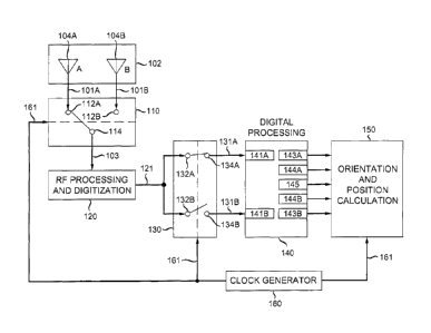
referred to as a base). In the measurement process, the coordinates of the
base
are known. The base contains a navigation receiver that receives satellite
signals. The coordinates of the base are precisely known (by GNSS, other
measurement schemes, or a combination of GNSS and other measurement
schemes).
[0004] The user, whose position is to be determined, may be stationary
or mobile and is often referred to as a rover. The rover also contains a
navigation receiver that receives satellite signals. Signal measurements
processed at the base are transmitted to the rover via a communications link.
The communications link, for example, may be provided over a cable or optical
fiber. To accommodate a mobile rover, the communications link is often a
wireless link. The rover processes the measurements received from the base,
along with measurements taken with its own receiver, to improve the accuracy
of
determining its position. Accuracy is improved in the differential navigation
mode
because errors incurred by the receiver at the rover and by the receiver at
the
base are highly correlated. Since the coordinates of the base are accurately
known, measurements from the base may be used to compensate for the errors
at the rover. A differential global positioning system (DGPS) computes
locations
based on pseudo-ranges only.
[0005] The location determination accuracy of a differential navigation
system may be further improved by supplementing the code pseudo-range
measurements with measurements of the phases of the satellite carrier signals.
If the carrier phases of the signals transmitted by the same satellite are
measured by both the navigation receiver in the base and the navigation
receiver
in the rover, processing the two sets of carrier phase measurements can yield
a
location determination accuracy to within several percent of the carrier's
wavelength. A differential navigation system that computes locations based on
2
CA 02767879 2012-01-11
WO 2011/007238
PCT/1B2010/001717
real-time carrier signals (in addition to the code pseudo-ranges) is often
referred
to as a real-time kinematic (RTK) system. Processing carrier phase
measurements to determine coordinates includes the step of ambiguity
resolution; that is, determining the integer number of cycles in the carrier
signal
received by the navigation receiver from an individual satellite.
[0006] To measure the rover heading, an antenna platform may be
mounted onto the rover. Several antennas separated from one another by user-
specified distances are installed on this platform. Since the antenna platform
is
tightly mounted to the rover housing, the orientation of the set of antennas,
which
can be determined by receiver measurements, unambiguously fixes the rover
heading as well.
[0007] When an individual antenna belongs to a set of antennas, the
individual antenna is referred to as an antenna unit. Each antenna unit,
independently of each other, receives a signal from all navigation satellites
in
view. The signals from all the antenna units are inputted to the navigation
receiver, where they are processed by tracking systems. A set of
measurements from all the antennas units and a number of satellites allows the
determination of the coordinates of the set of antenna units and also the
directions of lines between the separate antenna units (and, therefore, the
directions of axes for the antenna platform). To determine three angles
assigning the orientation of the platform plane, at least three antenna units
are
needed. To find the direction of one axis, two spaced-apart antenna units are
sufficient.
[0008] Previous technical publications have described different
systems for measuring angle coordinates based on signals from navigation
satellites. For example, U.S. Patent No. 4,881,080 describes a compass system
and method for determining heading. The compass system includes two
antennas located at a predetermined distance. Coordinates of each antenna are
separately determined by different navigation (GPS) receivers. A
microprocessor
computes and displays a compass heading on a display unit based on the
3
CA 02767879 2012-01-11
WO 2011/007238
PCT/1B2010/001717
knowledge of the coordinates of the two antennas and the distance between
them.
[0009] As the complexity of global navigation satellite systems has
grown, the number of satellites in view at any instant has increased. Separate
receiving and processing of signals transmitted from each satellite to each
antenna unit would require complicated navigation receivers. To simplify
receiver design, schemes have been developed that utilize successive switching
of a part of the receiver to different antenna units; a set of measurements
obtained at different time instants is used to determine heading. Such a
method
is described in U.S. Patent No. 5,917,448, which describes a common switch
that
successively connects each antenna unit to a common receiver. The duration of
time over which one antenna unit is connected to the receiver is such that all
transient processes in tracking systems are over, and the energy to make code
and phase measurements at a certain accuracy is stored to a sufficient degree.
In this case, the speed of switching should not be high and is selected within
a
range of a few Hz; consequently, the orientation of an antenna platform cannot
be accurately determined if the orientation is changing too quickly.
[0010] A number of patents, for instance, U.S. Patent No. 5,268,695
and U.S. Patent No. 6,154,170, specify one main (master) antenna and one
auxiliary (slave) antenna. Only the master antenna has tracking systems, and
it
is used for determination of the rover coordinates. The slave antenna does not
have tracking systems. Its phase measurements relative to reference signals
being formed in tracking loops for the master antenna are equivalent to the
phase difference of incoming signals in the master and slave antennas. Using
measurements for a number of satellites, the phase differences allow heading
determination of the set of antenna units.
[0011] U.S. Patent No. 4,719,469 describes a heading system in
which there is a common RF processing module for the separate antenna units
and a separate independent phase-lock loop (PLL) for each antenna unit. The
common RE processing module receives signals from the different antenna units
4
CA 02767879 2012-01-11
WO 2011/007238
PCT/1B2010/001717
at carrier frequency and converts them to an intermediate frequency. Each PLL
at the intermediate frequency tracks the signal from a corresponding antenna
unit
and measures carrier phase. A switch synchronously switches the common RF
processing module to the first antenna unit and first PLL and then to the
second
antenna unit and second PLL. Switching is sufficiently fast that each PLL
practically simultaneously estimates carrier phase from each antenna unit. The
phase difference between the first antenna unit and second antenna unit is
calculated; based on this difference, the heading angle of the set of antenna
units
is computed. Note that only one of the antenna units provides a signal for the
DLL, and rover coordinates are determined according to this antenna unit.
[0012] To determine the orientation of the set of antenna units, phase
measurements from different antenna units, the mutual positions of which are
known, are used in computations. Phase measurements according to signals
from navigation satellites, however, are unambiguous only over - 7-/- / 2. To
unambiguously determine orientation, it is necessary to resolve the
ambiguities.
[0013] To perform this task, the following approaches may be used:
= A distance between antenna units is selected that is smaller than
the wavelength of the received signal. This configuration provides
an unambiguous phase difference measured by different antenna
units.
= Antenna units are separated at a predetermined distance such that
the phase difference ambiguities of one antenna pair can be
resolved with measurements from another antenna pair. Such
methods are well established in designing interferometers.
If the distance between antenna units is arbitrary, resolution of phase
ambiguities
can be obtained by methods of integer minimization that is often used in
navigation receivers operating in the RTK mode. In this case, both phase and
code measurements are utilized for each antenna unit. To resolve ambiguities,
additional external, less-accurate, inclination sensors (such as a compass or
an
original checkpoint) may also be used.
CA 02767879 2015-07-02
[0014] What are needed are methods and apparatus for efficiently
processing signals transmitted by a constellation of global navigation
satellites and
received by a set of antenna units. Navigation receivers that reduce the
number of
hardware components and efficiently utilize the received signal energy are
advantageous.
BRIEF SUMMARY OF THE INVENTION
[0015] A navigation receiver processes signals transmitted by global
navigation satellites and received by a set of antenna units. Each individual
antenna
unit is connected to an individual input port of an antenna multiplexer
switch.
Satellite signals received from each individual antenna unit are consecutively
switched to a common output port of the antenna multiplexer switch. Satellite
signals received from the output port are processed by a common radiofrequency
processing module. A common signal correlator for different antenna units
generates a common in-phase correlation signal from the radiofrequency-
processed
signal. The common in-phase correlation signal is processed by a data
processing
module to demodulate information symbols from the received satellite signals.
The
common in-phase correlation signal is also processed by phase-lock loops and
delay-lock loops to generate carrier phases and code delays from the received
satellite signals. The common in-phase correlation signal utilizes the total
signal
power received from all antenna units for further signal processing.
[0015a] Certain exemplary embodiments can provide a navigation
receiver comprising: an antenna multiplexer switch configured to: sequentially
receive global navigation satellite system (GNSS) signals from each specific
antenna unit in a set of antenna units; and sequentially send the sequentially
received GNSS signals; a radiofrequency (RF) and digitization module
configured
to: sequentially receive all the GNSS signals sequentially sent by the antenna
multiplexer switch; and generate an output RF digital signal comprising a
sequence
of output RF digital signal segments, each specific output RF digital signal
segment
in the sequence of output RF digital signal segments corresponding to the GNSS
signals received from a specific antenna unit; and a common in-phase
correlator
6
CA 02767879 2015-07-02
configured to receive all the output RF digital signal segments and generate a
common in-phase correlation signal based at least in part on all the output RF
digital signal segments.
[0015b] Certain exemplary embodiments can provide a method for
processing global navigation satellite system (GNSS) signals received by a set
of
antenna units, the method comprising the steps of: sequentially receiving the
GNSS
signals from each specific antenna unit in the set of antenna units;
generating an
output radiofrequency (RF) digital signal comprising a sequence of output RF
digital
signal segments, each specific output RF digital signal segment in the
sequence of
output RF digital signal segments corresponding to the GNSS signals received
from
a specific antenna unit; and generating a common in-phase correlation signal
based
at least in part on all the output RF digital signal segments.
[0015c] Certain exemplary embodiments can provide an apparatus for
processing global navigation satellite system (GNSS) signals received by a set
of
antenna units, the apparatus comprising: means for sequentially receiving the
GNSS signals from each specific antenna unit in the set of antenna units;
means for
generating an output radiofrequency (RF) digital signal comprising a sequence
of
output RF digital signal segments, each specific output RF digital signal
segment in
the sequence of output RF digital signal segments corresponding to the GNSS
signals received from a specific antenna unit; and means for generating a
common
in-phase correlation signal based at least in part on all the output RF
digital signal
segments.
[0016] These and other advantages of the invention will be apparent
to
those of ordinary skill in the art by reference to the following detailed
description and
the accompanying drawings.
BRIEF DESCRIPTION OF THE DRAWINGS
[0017] Fig. 1A and Fig. 1B show a schematic of a navigation
receiver
in which signals from individual antenna units are separated at the inputs of
multiple
6a
CA 02767879 2012-01-11
WO 2011/007238
PCT/1B2010/001717
combined multipliers, and a common in-phase correlation signal is processed
for
phase-lock loop and delay-lock loop discriminators;
[0018] Fig. 2A ¨ Fig. 2C show a schematic of a navigation receiver
similar to that shown in Fig. 1A and Fig. 1B, except the signals from
different
antenna units are separated at the outputs of multiple combined multipliers
within
closed phase-lock loops and delay-lock loops;
[0019] Fig. 3A and Fig. 3B show a schematic of a navigation receiver
similar to that shown in Fig. 2A ¨ Fig. 2C, except signals from individual
antenna
units are separated at the outputs of accumulators within closed phase-lock
loops and delay-lock loops;
[0020] Fig. 4A ¨ Fig. 4C show a schematic of a navigation receiver in
which signals from individual antenna units are processed by a common
combined multiplier and common reference signal generators, and signals from
individual antenna units are separated at the outputs of the combined
multiplier
within closed phase-lock loops and delay-lock loops;
[0021] Fig. 5A ¨ Fig. 50 show a schematic of a navigation receiver
similar to that shown in Fig. 4A ¨ Fig. 40, except signals from individual
antenna
units are separated at the outputs of accumulators within closed phase-lock
loops and delay-lock loops;
[0022] Fig. 6A ¨ Fig. 60 show a schematic of a navigation receiver in
which signals from individual antenna units are processed with a common delay-
lock loop, and signals from individual antenna units are separated at the
outputs
of a common combined multiplier within closed phase-lock loops;
[0023] Fig. 7A ¨ Fig. 70 show a schematic of a navigation receiver
similar to that shown in Fig. 6A ¨ Fig. 60, except only the quadrature
correlation
signals from individual antenna units are separated at the outputs of an
accumulator within closed phase-lock loops;
[0024] Fig. 8 shows plots of the phase of the carrier numerically
controlled oscillator as a function of switching time; and
7
CA 02767879 2012-01-11
WO 2011/007238
PCT/1B2010/001717
[0025] Fig. 9 shows a flowchart of a method for processing satellite
signals received by a set of antenna units.
DETAILED DESCRIPTION
[0026] Each satellite in a global navigation satellite system may
transmit signals on more than one frequency band (for example, one signal on
the Li frequency band and one signal on the L2 frequency band). A signal
transmitted by a specific satellite on a specific frequency band constitutes a
specific satellite channel. Satellite channels are processed in a navigation
receiver as described below.
[0027] Radio signals received by an antenna are inputted into a
radiofrequency (RF) processing and digitization block, which includes input
amplifiers, filtering blocks, frequency converters, and analog-to-digital
converters
(ADCs). The digital signals are then processed in digital processing blocks
for
the satellite channels. The results of the digital processing are navigation
data.
Navigation data includes phase measurements, code measurements, and
information symbols used for solving navigation tasks.
[0028] Herein a block refers to a functional block. A set of
functional
steps may be grouped into user-specified blocks and sub-blocks. Herein, a
module refers to a user-specified set of hardware, firmware, and software
which
implements (executes) a user-specified set of functional steps. The same set
of
functional steps may be implemented by different user-specified modules (that
is,
different combinations of hardware, firmware, and software).
[0029] Processing steps that require high-speed execution are
typically
performed by hard-wired circuits [for example, application-specific integrated
circuits (ASICs) and field-programmable gate arrays (FPGAs)] and firmware.
Processing steps that do not require high-speed execution are typically
performed by a computational system including a microprocessor that executes
firmware-defined or software-defined program instructions. The computational
system is typically integrated into the navigation receiver.
8
CA 02767879 2012-01-11
WO 2011/007238
PCT/1B2010/001717
[0030] In processing each channel, two tracking systems track
changes in parameters of the received signal. The first tracking system,
referred
to as the delay-lock loop (DLL), tracks changes in the pseudo-random number
(PRN) modulation code delay of the received signal. The second tracking
system, referred to as the phase-lock loop (PLL), tracks changes in the
carrier
phase of the received signal.
[0031] In a tracking system, the input signal is multiplied by
different
reference signals generated in the receiver, and the multiplication products
are
accumulated. Devices that perform multiplication are referred to as
multipliers.
Devices that perform several combinations of multiplications are referred to
as
combined multipliers. Devices that perform accumulation are referred to as
accumulators or counters. Devices that perform multiplication followed by
accumulation are referred to as correlators. The output of a correlator is the
cross-correlation function of the input signal and the reference signal; for
simplicity, the output is referred to as the correlation signal.
[0032] A satellite channel is typically processed via three parallel
processing paths. The first path calculates the in-phase correlation signal I.
This signal is obtained when the reference signal in the correlator is in-
phase
relative to the incoming signal carrier. The reference code in the reference
signal
is a replica of the PRN code modulating the incoming signal. The output of
this
correlator (correlator-I) is the in-phase correlation signal I.
[0033] The phase of the reference signal can differ from that of the
carrier phase of the incoming signal; similarly, the reference code delay can
differ
from the modulation code delay of the incoming signal. If the phase shift
between the phase of the reference carrier and the phase of the incoming
carrier
is denoted as 0, and the time shift between the code delay time of the
reference
code and the code delay time of the incoming signal is denoted as r, then the
in-
phase correlation signal / can be approximated by:
9
CA 02767879 2012-01-11
WO 2011/007238 PCT/1B2010/001717
I = k -U = ,u = Ro(r)- cos(0) + ,
(El)
where:
R0(r) is the normalized cross-correlation function of the incoming
PRN code after filtering in the receiver RF module and a reference
code which is a locally generated copy of the PRN code modulating
the incoming signal;
U is the amplitude of the incoming signal;
= 1 is the binary information symbol modulating the incoming
signal;
k is a proportionality coefficient; and
is the interference at the output of correlator-/ caused by
additive interference at the receiver input.
[0034] The second correlator (correlator-Q) calculates the quadrature
correlation signal Q. This signal is obtained when the second reference
carrier
is shifted by 71" I 2 from the first reference carrier. The reference code is
the
same as the one in the first correlator (correlator-/). The quadrature
correlation
signal Q formed at the output of correlator-Q can be approximated by:
Q=k=Us- ,u = R 0(r) = sin(0) + Qin , (E2)
where an is the interference at the output of correlator-Q caused by additive
interference at the receiver input.
[0035] The third correlator (correlator-d/) calculates the code
correlation signal dl that is used to generate an error signal to control the
CA 02767879 2012-01-11
WO 2011/007238
PCT/1B2010/001717
system tracking modulation code delays (DLL). To obtain this signal, the first
reference carrier, in-phase with the input carrier, and a reference code that
consists of a sequence of short strobe pulses (strobe sequence) are used.
Strobe pulses correspond to the changes of sign of input PRN-code elements
(chips). Note that the sign of a strobe pulse matches the sign of a chip which
follows the strobe pulse. The code correlation signal dl can be approximated
by:
dI = k -U s p AR0(r) cos(0) + di in , (E3)
where Ak(r) is the cross-correlation function of the incoming PRN code after
passing through the receiver filter and the reference code generated in the
form
of a sequence of short strobe pulses, and di in is the interference at the
output
of correlator-d/ caused by the additive interference at the receiver input.
[0036] In the process of receiver operation, values in expressions
(El)
¨ (E3) are changed, and the corresponding correlation signals are changed
respectively. Correlation signals I, Q, and dl are used for coordinating (co-
working) the PLL and DLL tracking systems.
[0037] Expressions (El) ¨ (E3) hold under the condition that PLL
errors
0 and DLL errors V remain practically the same over the time (duration) of
accumulating in correlators. In tracking mode, this condition is true to an
adequate accuracy. In addition, in tracking mode, values 0 and V are small,
and R0 (r) = cos(0) 1. From (El), it follows that the in-phase correlation
signal I produces a binary information symbol sequence = 1. These
symbols convey messages from the navigation satellites to the navigation
receiver. The messages include satellite data on satellite coordinates,
expected
11
CA 02767879 2012-01-11
WO 2011/007238
PCT/1B2010/001717
parameters of signal propagation, and other information that is used for
coordinate determination.
[0038] The PLL and DLL digital tracking systems are implemented by
closed circuits comprising four main components: correlator, discriminator,
loop
filter, and numerically-controlled oscillator (NCO). Depending on the purpose
and type of the tracking system (PLL or DLL), these tracking systems use the
I,
Q , or dl correlation signals in different combinations. The correlators
include
combined multipliers that multiply the incoming signal by corresponding
reference signals and accumulators that accumulate corresponding
multiplication
products over a specified time interval. Combined multipliers multiply the
incoming signal by an in-phase reference carrier and reference code, by a
quadrature reference carrier and reference code, and by an in-phase reference
carrier and reference strobe.
[0039] A typical PLL discriminator forms an error signal UD according
to the algorithm:
=
UD = arctg(Q / I) . (E4)
From (El), (E2), and (E4), error signal UD is proportional to error 0 within
7C / 2, and then it periodically repeats. The mean value of UD(0) forms the
PLL discriminator characteristic. The error signal is inputted to the loop
filter,
which in turn outputs a control signal and closes the PLL circuit, thereby
controlling the frequency and phase of the PLL reference signal carrier NCO
(also referred to as the carrier NCO). The carrier NCO produces reference
signals for correlator-/ and correlator-Q.
[0040] The DLL circuit operates in a similar way and includes similar
components. The DLL discriminator forms tracking error VD using the
algorithm:
12
CA 02767879 2012-01-11
WO 2011/007238
PCT/1B2010/001717
VD dI I I . (E5)
The DLL reference signal code and strobe NCO (also referred to as the code and
strobe NCO) generates two reference signals (reference oscillations) for the
correlator-d/: one oscillation (code reference signal or code reference
oscillation)
in the form of a modulation code replica (or code sequence) to generate the in-
phase correlation signal I, and the other (strobe reference signal or strobe
reference oscillation) in the form of a strobe sequence which is sent to
correlator-
dI.
[0041] Discriminators operating according to expressions (E4) and (E5)
can be modified if the in-phase correlation signal / is subjected to a
preliminary
smoothing process to reduce the interference component I,,. Smoothing the in-
phase correlation signal / increases the operational stability of the tracking
loops at low signal-to-noise ratios.
[0042] The PLL tracking system tries to make the tracking error 0
equal to zero. As a result, one of the reference signals generated by the
carrier
NCO will be in-phase with the incoming signal, and its phase can be used to
estimate the carrier phase of the incoming signal. Such an estimate is called
a
phase measurement of the receiver.
[0043] The DLL tracking system tries to reduce the tracking error r to
zero. As a result, reference signals generated by the code and strobe NCO will
correspond to the modulation code of the incoming signal. Delays of these
reference signals can be used to estimate modulation code time delay of the
incoming signal. Such an estimate is called a code measurement of the
receiver.
[0044] Phase and code measurements obtained from signals of a
number of satellites are used to determine coordinates and receiver speed. Due
to external effects on tracking systems, the tracking errors fluctuate close
to
13
CA 02767879 2012-01-11
WO 2011/007238
PCT/1B2010/001717
steady balance points in which error signals are equal to zero. At normal
conditions in tracking modes, these errors are negligible. One source of
tracking
errors is the inertia of the tracking system. Another source of tracking
errors is
external radio interference that causes interference (in particular, noise)
errors.
Both types of errors depend on the inertia of the tracking system. In the
tracking
mode, the inertia can be estimated by the bandwidth of the equivalent filter,
operation of which is equivalent to the corresponding tracking circuit (loop).
The
bandwidth of this filter characterizes the inertia of the tracking system and
its
filtering parameters. The bandwidth should be chosen based on a trade off
between dynamic and noise errors.
[0045] When a navigation receiver receives satellite signals from a set
of antenna units, the navigation receiver also calculates the orientation of
the set
of antenna units. If the set of antenna units includes only two antenna units,
the
orientation is determined by two angles specifying the orientation of a base
line
between the two antenna units. If the set of antenna units includes three
antenna units, the orientation is determined by three angles specifying the
orientation of a base plane passing through the three antenna units. The
accuracy of determining the angles increases as the distances between antenna
units increase.
[0046] One of several embodiments of a navigation system is shown in
Fig. 1A and Fig. 1B. Fig. 1A shows the overall architecture of a navigation
system comprising a set of antenna units and a navigation receiver. The set of
antenna units 102 includes antenna unit A 104A and antenna unit B 104B. The
antenna units are spaced apart (spatially separated by a distance). To
simplify
the discussion and figures, the set of antenna units 102 is shown with only
two
antenna units. In general, however, the set of antenna units 102 may have N
antenna units, where N is an integer greater than or equal to 2. The RF signal
101A (corresponding to satellite signals received from multiple global
navigation
satellites) received from antenna unit 104A is fed into input port 112A of
antenna
multiplexer switch 110. Similarly, the RF signal 101B (corresponding to
satellite
14
CA 02767879 2012-01-11
WO 2011/007238
PCT/1B2010/001717
signals received from multiple global navigation satellites) received from
antenna
unit 104B is fed into input port 112B. In general, antenna multiplexer switch
110
has N input ports, one for each of the N antenna units.
[0047] The output RF signal 103 from output port 114 of antenna
multiplexer switch 110 is fed into RF processing and digitization block 120,
where
RF processing and digitization block 120 refers to a functional block. As
discussed above, the RF processing and digitization block is implemented by a
RF processing and digitization module. The output RF signal 103 is
sequentially
switched between input RF signal 101A and input RF signal 101B in response to
clock signal 161 from clock generator 160.
[0048] The output RF-processed and digitized signal 121 from RF
processing and digitization block 120 is fed simultaneously into input port
132A
and input port 132B of separator switch 130. To simplify the terminology,
output
RF-processed and digitized signal 121 is also referred to as output RF digital
signal 121. Herein, the output RF digital signal comprises output RF digital
segments, each specific output RF digital segment corresponding to a specific
antenna unit. The circuit path between input port 132A and output port 134A of
separator switch 130 is opened/closed in response to clock signal 161.
Similarly,
the circuit path between input port 132B and output port 134B of separator
switch
130 is closed/opened in response to clock signal 161.
[0049] Operation of antenna multiplexer switch 110 and separator
switch 130 is synchronized. When antenna multiplexer switch 110 is switched to
input port 112A, separator switch 130 is switched such that the circuit path
between input port 132A and output port 134A is closed, and the circuit path
between input port 132B and output port 134B is open. Similarly, when antenna
multiplexer switch 110 is switched to input port 112B, separator switch 130 is
switched such that the circuit path between input port 132A and output port
134A
is open, and the circuit path between input port 132B and output port 134B is
closed. The output signal 131A from output port 134A is fed into input port
141A
of digital processing block 140, where digital processing block 140 refers to
a
CA 02767879 2012-01-11
WO 2011/007238
PCT/1B2010/001717
functional block. Similarly, the output signal 131B from output port 1346 is
fed
into input port 141B of digital processing block 140.
[0050] Output 143A, output 144A, output 145, output 144B, and output
143B of digital processing block 140 are fed into orientation and position
calculation block 150, where orientation and position calculation block 150
refers
to a functional block. Clock signal 161 is also inputted into orientation and
position calculation block 150.
[0051] Details of orientation and position calculation block 150 are
not
provided, since well-known techniques can be used to calculate orientation and
position from the input values. Methods for calculating positions are
discussed,
for example, in B. W. Parkinson and J.J. Spilker, "Global Positioning System:
Theory and Application," American Institute of Aeronautics and Astronautics,
Washington DC, 1996, and B. Hofmann-Wellenhof, H. Lichtenegger, and
J.Collins, "Global Positioning System: Theory and Practice," Springer,
Wien/NewYork, 1992. Methods for calculating orientations are based on the fact
that the phase difference A0 is related to angle 0 according to
2.A 2.P.L.cos(8)2.ir.Lcos(s)cos(fl)where2is
the wavelength, Ac/5 is the phase difference between two antennas, L is the
distance between two antennas (the modulus of the vector L which connects
two antennas), 0 is the spatial angle between the signal reception vector and
the vector between two antennas, and (s,16) are the orientation angles
(elevation and azimuth angles) of vector L. A solution of a set of the
equations
with measurements for different satellites can help in finding angles E and
,8.
Methods for ambiguity resolution are described, for example, in U.S. Patent
No.
7,102,563.
[0052] Fig. 1B shows a functional schematic of digital processing
block
140. Digital processing block 140 includes delay-lock loop (DLL) tracking
16
CA 02767879 2012-01-11
WO 2011/007238
PCT/1B2010/001717
systems for measuring code delays and phase-lock loop (PLL) tracking systems
for measuring carrier phase. Separate DLL and PLL tracking systems are
provided for input signals from antenna unit A 104A and antenna unit B 104B.
Herein, systems and system elements (including functional blocks, sub-blocks,
and components) correspond to satellite signals received by antenna unit A
104A
if they process input signals from antenna unit A 104A. Similarly, systems and
system elements (including functional blocks, sub-blocks, and components)
correspond to satellite signals received by antenna unit B 104B if they
process
input signals from antenna unit B 104B.
[0053] Digital processing block 140 is partitioned into three digital
processing sub-blocks. Digital processing sub-block 142A is dedicated to
processing signals from antenna unit A 104A. Digital processing sub-block 142B
is dedicated to processing signals from antenna unit B 104B. Note that
corresponding elements in digital processing sub-block 142A and digital
processing sub-block 142B are labelled XXXA and XXXB, respectively, where
XXX is a three-digit reference number. Digital processing sub-block 142C is a
common digital processing sub-block that processes signals from both antenna
unit A 104A and antenna unit B 104B.
[0054] The tracking systems for the signals from antenna unit A 104A
are implemented by digital processing sub-block 142A and digital processing
sub-block 142C. The tracking systems for the signals from antenna unit B 104B
are implemented by digital processing sub-block 142B and digital processing
sub-block 142C. The tracking systems for signals from antenna unit A 104A are
described below. A similar description applies for the tracking systems for
signals from antenna unit B 104B.
[0055] Refer to Fig. 1A. In response to clock signal 161, antenna
multiplexer switch 110 is set to select input RF signal 101A from antenna unit
104A for processing in RF processing and digitization block 120. The output RF
digital signal 121 from RF processing and digitization block 120 is then
selected
by separator switch 130 for processing in digital processing block 140.
17
CA 02767879 2012-01-11
WO 2011/007238
PCT/1B2010/001717
[0056] Refer to Fig. 1B. Output signal 131A from separator switch 130
is inputted into input 141A of combined multiplier 174A, which also receives
reference signals from carrier numerically controlled oscillator (NCO) 176A
and
reference signals from code and strobe NCO 172A. Combined multiplier 174A
multiplies input signal 131A by an in-phase reference code. The corresponding
output of combined multiplier 174A is labelled iA and referred to as the in-
phase
multiplier output. The in-phase multiplier output iA is accumulated in
accumulator 190. In Fig. 1B, and other figures, the E symbol refers to an
accumulator. The output of accumulator 190 is the in-phase correlation signal
I, which is inputted into data processing module 192, DLL discriminator 182A,
DLL discriminator 182B, PLL discriminator 184A, and PLL discriminator 184B.
Further processing of I is described below. The output of data processing
module 192 is sent to orientation and position calculation block 150.
[0057] Combined multiplier 174A multiplies the input signal 131A by a
quadrature-phase reference carrier. The corresponding output of combined
multiplier 174A is labelled qA and referred to as the quadrature multiplier
output.
The quadrature multiplier output qA is accumulated in accumulator 180A. The
output of accumulator 180A is the quadrature correlation signal QA, which is
inputted into PLL discriminator 184A. in Fig. 1B, and other figures, the U D
symbol refers to a PLL discriminator. The output of PLL discriminator 184A is
inputted into PLL loop filter (LF) 188A. The output of PLL loop filter 188A is
sent
to orientation and position calculation block 150. The output of PLL loop
filter
188A is also sent as an input control signal to carrier NCO 176A.
[0058] Combined multiplier 174A multiplies input signal 131A by strobe
pulses. The corresponding output of combined multiplier 174A is labelled diA
and referred to as the code multiplier output. The code multiplier output diA
is
18
CA 02767879 2012-01-11
WO 2011/007238
PCT/1B2010/001717
accumulated in accumulator 178A. The output of accumulator 178A is the code
correlation signal diA , which is inputted into DLL discriminator 182A. In
Fig. 1B,
and other figures, the VD symbol refers to a DLL discriminator. The output of
DLL discriminator 182A is inputted into DLL loop filter 186A. The output of
DLL
loop filter 186A is sent to orientation and position calculation block 150.
The
output of DLL loop filter 186A is also sent as an input control signal to code
and
strobe NCO 172A.
[0059] Combined multiplier 174A, carrier NCO 176A, code and strobe
NCO 172A, accumulator 178A, accumulator 180A, and accumulator 190 are
typically implemented in hardware [for example, in application-specific
integrated
circuits (ASICs)] for high-speed operation. PLL discriminator 184A, DLL
discriminator 182A, PLL loop filter 188A, and DLL loop filter 186A typically
operate at a sufficiently low speed that they may be implemented by a
microprocessor.
[0060] In the embodiment shown in Fig. 1B, there are five
accumulators. Two are dedicated for processing signals from antenna unit A
104A: accumulator 178A for dIA and accumulator 180A for QA Similarly,
two are dedicated for processing signals from antenna unit B 104B: accumulator
178B for dIB and accumulator 180B for QB' Accumulator 190, however,
stores the in-phase correlation signal / from both antenna unit 104A and
antenna unit B 104B.
[0061] When the PLL and DLL are operating in steady-balance tracking
modes, the in-phase correlation signal / does not substantially depend on the
antenna unit selected; therefore, irrespective of the switching state of
antenna
multiplexer switch 110 and separator switch 130, I can be averaged over time
intervals considerably exceeding the operational period of the clock generator
160. Using a common accumulator 190 for the in-phase correlation signal I,
and averaging its value over a symbol duration, enables the total signal
energy
19
CA 02767879 2012-01-11
WO 2011/007238
PCT/1B2010/001717
received by the set of antenna units 102 to be utilized for isolating
information
symbols in data processing block 192. The output of the common accumulator
190 is referred to herein as the common in-phase correlation signal I.
[0062] The common in-phase correlation signal / from accumulator
190 is also inputted into PLL discriminator 184A, DLL discriminator 182A, PLL
discriminator 184B, and DLL discriminator 182B for generating PLL and DLL
discrimination characteristics. As discussed earlier, to enhance operational
stability of the tracking loops at low signal-to-noise ratios, the common in-
phase
correlation signal / may be processed by an additional smoothing step (not
shown). The use of a common accumulator 190 for the common in-phase
correlation signal I also allows utilization of the total signal energy
received by
the set of antennas 102; therefore, the operational stability of the PLL and
the
DLL at low signal-to-noise ratios is further increased.
[0063] The following outputs are generated by digital processing block
140:
= Output 143A from DLL loop filter 186A is the set of code delay
measurements for antenna unit A 104A;
= Output 144A from PLL loop filter 188A is the set of carrier phase
measurements for antenna unit A 104A;
= Output 143B from DLL loop filter 186B is the set of code delay
measurements for antenna unit B 104B;
= Output 144B from PLL loop filter 188B is the set of carrier phase
measurements for antenna unit B 104B; and
= Output 145 from data processing block 192 is the set of satellite
data.
CA 02767879 2012-01-11
WO 2011/007238
PCT/1B2010/001717
These outputs are sent to orientation and position calculation block 150 (Fig.
1A),
which calculates the orientation and position of the rover on which the set of
antenna units 102 are mounted.
[0064] As discussed above, the generation of a common in-phase
correlation signal I for multiple antenna units is implemented when the
tracking
systems operate in a steady-balance mode. The lock-on mode precedes the
steady-balance mode. In the lock-on mode, the common in-phase correlation
signal I does not need to be used: for each individual antenna unit, the
corresponding individual in-phase correlation signal is used for signal
acquisition
by the corresponding individual tracking system.
[0065] Another embodiment is shown in Fig. 2A and Fig. 2B. The
overall system architecture, shown in Fig. 2A, is similar to the overall
system
architecture shown previously in Fig. 1A. In this embodiment, the output RF
digital signal 121 from RF processing and digitization block 120 is fed
simultaneously into input 141A and input 141B of digital processing block 240.
Output 143A, output 144A, output 145, output 144B, and output 143B from
digital
processing block 240 are sent to orientation and position calculation block
150.
As described in detail below, the inputs and outputs of digital processing
block
240 are the same as those of digital processing block 140; therefore, they are
labelled by the same reference numbers. Clock signal 161 is inputted into
input
230 of digital processing block 240.
[0066] Refer to Fig. 2B. The architecture of digital processing block
240 is similar to that of digital processing block 140 (Fig. 1B). Digital
processing
block 240 is partitioned into three digital processing sub-blocks. Digital
processing sub-block 242A is dedicated to processing signals from antenna unit
A 104A. Digital processing sub-block 242B is dedicated to processing signals
from antenna unit B 104B. Digital processing sub-block 242C is a common sub-
block that processes signals from both antenna unit A 104A and antenna unit B
104B.
21
CA 02767879 2012-01-11
WO 2011/007238
PCT/1B2010/001717
[0067] The digital processing in digital processing block 240 is
similar
to that in digital processing block 140. Only the differences are described.
In
Fig. 2B, the output RF digital signal 121 from RF processing and digitization
block 120 is inputted simultaneously into input 141A of combined multiplier
174A
and input 141B of combined multiplier 174B. Refer now to the digital
processing
within digital processing sub-block 242A. The outputs of combined multiplier
174A, labelled in-phase multiplier output iA , quadrature multiplier output qA
,
A
J=
and code multiplier output di A, are fed into input ports of separator switch
250A.
As shown in Fig. 2A, the output RF digital signal 121 from RF processing and
digitization block 120 is fed into input 141A of combined multiplier 174A
irrespective of the switching state of antenna multiplexer switch 110.
Separation
of multiplier outputs derived from antenna unit A 104A and from antenna unit
104B is performed by separator switch 250A. Herein, each multiplier output
comprises multiplier output segments, each specific multiplier output segment
corresponding to a specific antenna unit.
[0068] When signals from antenna unit A 104A are tracked, separator
switch 250A is closed, and separator switch 250B is open. Fig. 20 shows a
detailed view of separator switch 250A. The outputs from combined multiplier
A
J= =A
174A, explicitly labelled al 261A, qA 263A, and / 265A, are fed into input
port 260A, input port 262A, and input port 264A, respectively, of separator
switch
250A. The corresponding output ports are output port 270A, output port 272A,
and output port 274A, respectively. Separator switch 250A is operated in
response to clock signal 161. When separator switch 250A is closed, the
corresponding output signals, code multiplier output diA 271A, quadrature
multiplier output qA 273A, and in-phase multiplier output iA 275A,
respectively,
are fed into accumulator 178A, accumulator 180A, and accumulator 190,
respectively. The output signals from accumulator 178A, accumulator 180A, and
22
CA 02767879 2012-01-11
WO 2011/007238
PCT/1B2010/001717
accumulator 190 are code correlation signal d/A 281A, quadrature correlation
signal QA 283A, and in-phase correlation signal I 285AB, respectively. The
output of accumulator 190 is labelled / 285AB because it accumulates signals
from both antenna unit 104A and antenna unit B 104B.
[0069] Separator switch 250B is configured similar to that of
separator
switch 250A, and signals from antenna unit B 104B are tracked similar to the
signals from antenna unit 104A. Digital processing in digital processing block
240 then proceeds as in digital processing block 140. In some instances, the
switching configuration shown in Fig. 2A ¨ Fig. 2C may be advantageous for
hardware and ASIC development, relative to the switching configuration shown
in
Fig. 1A and Fig. 1B.
[0070] Another embodiment is shown in Fig. 3A and Fig. 3B. The
overall system architecture, shown in Fig. 3A, is similar to that shown in
Fig. 2A,
except that the internal structure of digital processing block 340 is
different from
that of digital processing block 240. Details of digital processing block 340
are
shown in Fig. 3B. Digital processing block 340 is partitioned into three
digital
processing sub-blocks. Digital processing sub-block 342A is dedicated to
processing signals from antenna unit A 104A. Digital processing sub-block 342B
is dedicated to processing signals from antenna unit B 104B. Digital
processing
sub-block 342C is a common sub-block that processes signals from both
antenna unit A 104A and antenna unit B 104B.
[0071] Refer now to the digital processing within digital processing
sub-
block 342A. The outputs of combined multiplier 174A (code multiplier output
diA , quadrature multiplier output qA , and in-phase multiplier output lA )
are
inputted into accumulator 360A, accumulator 362A, and accumulator 364A,
respectively. The outputs of the accumulators are fed into input ports of
separator switch 350A.
[0072] The output ports of the accumulators are coupled to screening
blocks (SCRs), details of which are discussed below. When separator switch
23
CA 02767879 2012-01-11
WO 2011/007238
PCT/1B2010/001717
350A is closed, the output of accumulator 360A is fed into the input of
screening
block 370A, the output of accumulator 362A is fed into the input of screening
block 372A, and the output of accumulator 364A is fed into the input of
screening
block 374A.
[0073] The mode of operation of separator switch 350A is similar to
that of separator switch 250A in Fig. 2B and Fig. 2C. In response to clock
signal
161, separator switch 350A connects/disconnects the PLL and DLL tracking
systems in synchronization with antenna multiplexer switch 110 (Fig. 3A).
After
each switching cycle of antenna multiplexer 110, the first values of the
correlation
signals I, Q, and dl at the outputs of accumulator 364A, accumulator 362A,
and accumulator 360A, respectively, will not be true, since the accumulators
will
include stored values from both antenna unit A 104A and antenna unit B 104B.
These invalid values of the correlation signals I, Q, and dl are eliminated by
screening block 374A, screening block 372A, and screening block 370A,
respectively. Herein, the correlation signal at the output of an accumulator
comprises correlation signal segments, each specific correlation signal
segment
corresponding to a specific antenna unit. For eliminating invalid correlation
signals, screening block 374A, screening block 372A, and screening block 370A
should have information concerning the times at which separator switch 350A is
closed. Connections providing this information between clock generator 160 and
screening block 374A, screening block 372A, and screening block 370A are not
shown.
[0074] A screening block may be implemented by a switch that
operates synchronously with antenna multiplexer switch 110. The switch
disconnects the processing circuit when the first value of the correlation
signal
after the antenna multiplexer switch 110 has been switched reaches the
screening block. The switch then closes for the remainder of the sequence. For
example, if the screening block receives the input quadrature correlation
signal
sequence (k-values are received after each switching operation)
24
CA 02767879 2012-01-11
WO 2011/007238
PCT/1B2010/001717
¨÷Q11Q2/Q3,¨*Q1c,Q11Q2 1Q3)-91c,Q11Q2)Q3,¨Q10¨;
then the output of the screening block is the sequence
===, Q21Q3 5 = = = Qk ___--)Q2,Q31*==Qk) __,Q27Q3,= "Qk,= = = '
The first value Q1 of each sequence has been eliminated.
[0075] The processing of correlation signals to eliminate invalid
measurements degrades the tracking characteristics in the embodiment shown in
Fig. 3A and Fig. 3B relative to the embodiment shown in Fig. 2A ¨ Fig. 2C.
This
degradation, however, can be minimized by optimizing the switching parameters
for antenna multiplexer switch 110 and by optimizing the storage times of
correlation signals in accumulator 364A, accumulator 362A, and accumulator
360A. The embodiment shown in Fig. 3A and Fig. 3B can be useful for receiver
designs which use existing hardware (such as commercially available ASICs) to
implement various elements of digital processing block 342A: for example,
combined multiplier 174A, carrier NCO 176A, code and strobe NCO 172A,
accumulator 364A, accumulator 362A, and accumulator 360A.
[0076] In the embodiment shown in Fig. 3B, note that the common in-
phase correlation signal I is generated by two accumulators (accumulator 364A
and accumulator 364B). The common in-phase
correlation signal I is generated at summing junction 390 by summing 'A' the
in-phase correlation signal corresponding to antenna unit 104A, and 4, the in-
phase correlation signal corresponding to antenna unit 104B. In this
embodiment, the common in-phase correlator includes combined multiplier 174A,
accumulator 364A, combined multiplier 174B, accumulator 364B, and summing
junction 390.
[0077] As new GNSSs are developed and deployed, the number of
satellites and received signals increases. In the embodiments described above,
a receiver has a separate digital processing block to perform correlation
processing for each corresponding satellite system. Consequently, an increase
CA 02767879 2012-01-11
WO 2011/007238
PCT/1B2010/001717
in the number of functional digital processing blocks results in an increase
in the
number of hardware modules. As the number N of antenna units increases, the
number of hardware modules and the overall complexity of the hardware
increase further. Embodiments described below utilize hardware more
efficiently.
[0078] The overall architecture of the embodiment shown in Fig. 4A
comprises a set of antenna units 102, an antenna multiplexer switch 110, a
clock
generator 160, a digital processing block 440, and an orientation and position
calculation block 150. Digital processing block 440 is partitioned into
digital
processing sub-block 442 and digital processing sub-block 444. The output RF
digital signal 121 from the RF processing and digitization block 120 is fed
into
input 441 of digital processing sub-block 442. The clock signal 161 from clock
generator 160 is sent to antenna multiplexer switch 110 and orientation and
position calculation block 150. The clock signal 161 is also fed into input
430 of
digital processing sub-block 442. Output 401A, output 401B, output 403, output
404A, and output 404B of digital processing sub-block 442 are sent to input
411A, input 411B, input 413, input 414A, and input 414B of digital processing
sub-block 444, respectively. Output 416A, output 416B, output 418A, and output
418B of digital processing sub-block 444 are sent to input 406A, input 406B,
input 408A, and input 408B of digital processing sub-block 442, respectively.
Output 421A, output 422, output 423A, output 421B, and output 423B of digital
processing sub-block 444 are sent to orientation and position calculation
block
150.
[0079] In the previous embodiments discussed above, signals from
each individual antenna unit were processed by corresponding individual
hardware modules. In contrast, in the embodiment shown in Fig. 4A ¨ Fig. 4C,
the number of hardware modules does not depend on the number of antenna
units in the set of antenna units 102. Refer to Fig. 4B and Fig. 4C for
details of
digital processing block 440. The output RF digital signal 121 from RF
processing and digitization block 120 is fed into input port 441 of a single
(common) combined multiplier 450. Reference signals for all incoming antenna
26
CA 02767879 2012-01-11
WO 2011/007238
PCT/1B2010/001717
signals are generated by a single (common) carrier NCO 454 and a single
(common) code and strobe NCO 452.
[0080] The outputs of the combined multiplier 450 are the in-phase
multiplier output i, the quadrature multiplier output q, and the code
multiplier
output di. The quadrature multiplier output q is fed into input port 462 of
separator switch 460. In response to clock signal 161, the output of separator
switch 460 switches between output port 464A and output port 464B. Similarly,
the code multiplier output di is fed into input port 472 of separator switch
470.
In response to clock signal 161, the output of separator switch 470 switches
between output port 474A and output port 474B. Antenna multiplexer switch
110, separator switch 460, and separator switch 470 operate synchronously.
[0081] When the signals from antenna unit A 104A are being
processed, the output of separator switch 460 is switched to output port 464A.
The corresponding quadrature multiplier output qA is inputted into accumulator
4102A. The output of accumulator 4102A (quadrature correlation signal QA) is
processed successively by discriminator 4104A and PLL loop filter 4106A. The
output of PLL loop filter 4106A is sent to orientation and position
calculation block
150. Similarly, the output of separator switch 470 is switched to output port
474A. The corresponding code multiplier output diA is inputted into
accumulator 4110A. The output of accumulator 4110A (code correlation signal
d/A ) is processed successively by discriminator 4112A and DLL loop filter
4114A. The output of DLL loop filter 4114A is sent to orientation and position
calculation block 150.
[0082] When the signals from antenna unit B 104B are being
processed, the output of separator switch 460 is switched to output port 464B,
and the corresponding quadrature multiplier output qB is inputted into
accumulator 4102B. The output of accumulator 4102B (quadrature correlation
27
CA 02767879 2012-01-11
WO 2011/007238
PCT/1B2010/001717
signal QB) is processed successively by discriminator 4104B and PLL loop
filter
4106B. The output of PLL loop filter 4106B is sent to orientation and position
calculation block 150. Similarly, the output of separator switch 470 is
switched to
output port 474B, and the corresponding code multiplier output diB is inputted
into accumulator 4110B. The output of accumulator 4110B (code correlation
signal d/B ) is processed successively by discriminator 4112B and DLL loop
filter 4114B. The output of DLL loop filter 4114B is sent to orientation and
position calculation block 150.
[0083] The in-phase multiplier output i is not switched. It is
inputted
into accumulator 456. The output of accumulator 456 (common in-phase
correlation signal ) is inputted into data processing block 192. The output of
data processing block 192 is sent to orientation and position calculation
block
150.
[0084] Input control signals are fed into code and strobe NCO 452 and
carrier NCO 454 via commutator switch 480 and commutator switch 490,
respectively. Antenna multiplexer switch 110, commutator switch 480, and
commutator switch 490 operate synchronously.
[0085] An input control signal is fed into code and strobe NCO 452
from output port 482 of commutator switch 480. In response to clock signal
161,
output port 482 can be switched between input port 484A and input port 484B.
When signals from antenna unit A 104A are being processed, the input of
commutator switch 480 is switched to input port 484A, and the input control
signal is the output of DLL loop filter 4114A processed by extrapolator 4116A.
When signals from antenna unit B 104B are being processed, the input of
commutator switch 480 is switched to input port 484B, and the input control
signal is the output of DLL loop filter 4114B processed by extrapolator 4116B.
Details of extrapolators are discussed below.
[0086] Similarly, an input control signal is fed into carrier NCO 454
from
output port 492 of commutator switch 490. In response to clock signal 161,
28
CA 02767879 2012-01-11
WO 2011/007238
PCT/1B2010/001717
output port 492 can be switched between input port 494A and input port 494B.
When signals from antenna unit A 104A are being processed, the input of
commutator switch 490 is switched to input port 494A, and the input control
signal is the output of PLL loop filter 4106A processed by extrapolator 4118A.
When signals from antenna unit B 104B are being processed, the input of
commutator switch 490 is switched to input port 494B, and the input control
signal is the output of PLL loop filter 4106B processed by extrapolator 4118B.
[0087] The function of an extrapolator is discussed with reference to
the plots in Fig. 8. The example shows extrapolation of the input control
signal
to the carrier NCO 454. The horizontal (t) axis 802 represents the time t; the
vertical (0) axis 804 represents the phase 0 . Along the t -axis are shown a
sequence of equally spaced reference times (t1 810, t . 812, t1+1 . 814, t1+2
j-
816). The interval between neighboring reference times is At 860. Plot 830
(dashed line segments) represents the phase 0A of the signals from antenna A
104A. Plot 832 (dotted line segments) represents the phase OB of the signals
from antenna B 104B. Plot 840 (solid line segments) represents the phase
ONC01. To simplify the notation, ONC01 refers to the phase of the carrier NCO
454. The slope of 0A as a function of t is the frequency WA 850, and the slope
of OB as a function of t is the frequency COB 852. Shown are representative
values of phases at specific reference times: q5 (t+1) 828, OA (t1)826,
OB(t j+2) 824, 0B(t j+i) 822, and 10B(ti) 820.
[0088] The antenna multiplexer switch 110 is switched at the reference
times (t1-1' t1, t1+1' tj ). In the following discussion, these reference
times
+2
are also referred to as switching times. During the interval from t to
29
CA 02767879 2012-01-11
WO 2011/007238
PCT/1B2010/001717
signals from antenna A 104A are processed, andshould match OA.
ONC01
During the interval from ti to t1+1, signals from antenna B 104B are
processed,
andhld match B During the interval f t
sou B . urng erom . o t _
ONC01j+1 t signals j+2'
from antenna A 104A are processed, and ONC01 should match OA.
[0089] At each switching time, carrier NCO 454 needs to generate a
reference oscillation with the correct phase and frequency for the new
received
signals. Extrapolation is used to calculate the correct values for the next
interval
after switching. If the acceleration of an antenna unit in motion is
negligible, the
frequency CO may be assumed to be constant over an interval At, and linear
extrapolation may be used. As an example, consider the case in which antenna
multiplexer switch 110 is switched from antenna B 104B to antenna A 104A at
switching time till . At the moment of switching, NCQ(t 1+1) is set to
B (t1+1) Just after switching, ONC0(1-1+1) needs to be set to 0 A(1 1+1)
(assuming that the switching time is negligible). Just after switching at
switching
time t , the value of ONcoi was previously set to OA: ONC01(t 1) =A j (t ")
'
Therefore, the value ofONC01 (11+1)
(just after switching) may be calculated by
the following extrapolation algorithm:
ONCO(t j+1) = ONCO(t j) At a/NCO;
CO CO =
NCO =A,
0Ara)(t j) = 0A(t j)=
The extrapolated value is recorded in carrier NCO 454. A similar extrapolation
is
performed when the antenna multiplexer switch 110 is switched from antenna
CA 02767879 2012-01-11
WO 2011/007238
PCT/1B2010/001717
unit A 104A to antenna unit B 104B (for example, at switching time t12).
Extrapolated values of carrier frequency and phase for the current time are
sent
to carrier NCO 454 as input control signals. If the frequency CO is not
constant
over the interval At, square extrapolation (using a quadratic function) may be
used.
[0090] The extrapolator for the code and strobe NCO 452 operates in a
similar manner:
NCO2 (t j+1 = NCO2 (tj );
NCO2 0.
N C 0 2 (t j) = r A (tj)
Here, T is the code delay, and T' is the derivative of T with respect to t. To
simplify the notation, T Nco2 refers to the code delay of the code and strobe
NCO 454, and TA refers to the code delay of signals from antenna unit A 104A.
Note that in most practical cases, the rate of code delay change over the
interval
At is negligible and may be set to zero. If the distance between antenna units
is much shorter than pseudo-range measurement errors, then the code and
strobe NCO extrapolator does not need to be used, since delay changes can be
neglected when the antenna units are switched. In general, extrapolated values
of code delay for the current time are sent to code and strobe NCO 452 as
input
control signals.
[0091] Extrapolated carrier phase and frequency are calculated for the
instant of disconnecting the PLL and recorded in the carrier NCO 454 at the
instant of connecting the PLL. Carrier NCO 454 should provide independent
control both in phase and frequency. In an embodiment, PLL loop filter 4106A
and PLL loop filter 4106B are implemented by second order filters. Clock
generator 160 determines the instants of disconnecting and connecting the PLL
31
CA 02767879 2012-01-11
WO 2011/007238
PCT/1B2010/001717
and determines the pause duration necessary for operating extrapolator 4116A,
extrapolator 4116B, extrapolator 4118A, and extrapolator 4118B. Connections
between clock generator 160 and the extrapolators are not shown in the
figures.
[0092] In the embodiment shown in Fig. 4A - Fig. 4C, the combined
multiplier 450, carrier NCO 454, and code and strobe NCO 452 are normally
implemented in hardware. Since they process all signals received from the set
of
antenna units 102, the number of hardware modules is independent of the
number N of antenna units. Hardware utilization is therefore increased.
[0093] Fig. 5A - Fig. 5C show another embodiment. The overall
architecture, shown in Fig. 5A, is similar to that shown in Fig. 4A, except
the
internal structure of digital processing block 540 is different from that of
digital
processing block 440. Digital processing block 540 is partitioned into digital
processing sub-block 542 and digital processing sub-block 544. The output RF
digital signal 121 from the RF processing and digitization block 120 is fed
into
input 541 of digital processing sub-block 542. The clock signal 161 from clock
generator 160 is fed into input 530 of digital processing sub-block 442 and
into
input 532 of digital processing sub-block 544. Output 501A, output 501B,
output
503, output 504A, and output 504B of digital processing sub-block 542 are sent
to input 511A, input 511B, input 513, input 514A, and input 514B of digital
processing sub-block 544, respectively. Output 516A, output 516B, output 518A,
and output 518B of digital processing sub-block 544 are sent to input 506A,
input
506B, input 508A, and input 508B of digital processing sub-block 542,
respectively. Output 521A, output 522, output 523A, output 521B, and output
523B of digital processing sub-block 544 are sent to orientation and position
calculation block 150.
[0094] Refer to Fig. 5B and Fig. 50 for details of digital processing
block 540. The outputs of the combined multiplier 550 are the in-phase
multiplier
output i, the quadrature multiplier output q, and the code multiplier output
di.
These multiplier outputs are fed into accumulator 562, accumulator 560, and
accumulator 564, respectively. The output of accumulator 560 (quadrature
32
CA 02767879 2012-01-11
WO 2011/007238
PCT/1B2010/001717
correlation signal Q) is fed into input port 572 of separator switch 570. In
response to clock signal 161, the output of separator switch 570 switches
between output port 574A and output port 574B. Similarly, the output of
accumulator 564 (code correlation signal dl) is fed into input port 582 of
separator switch 580. In response to clock signal 161, the output of separator
switch 580 switches between output port 584A and output port 584B. Antenna
multiplexer switch 110, separator switch 570, and separator switch 580 operate
synchronously.
[0095] When the signals from antenna unit A 104A are being
processed, the output of separator switch 570 is switched to output port 574A,
and the quadrature correlation signal QA is processed successively by
screening block 5106A, discriminator 5108A, and PLL loop filter 5110A. The
output of PLL loop filter 5110A is sent to orientation and position
calculation block
150. Similarly, the output of separator switch 580 is switched to output port
584A, and the code correlation signal diA is processed successively by
screening block 5114A, discriminator 5116A, and DLL loop filter 5118A. The
output of DLL loop filter 5118A is sent to orientation and position
calculation
block 150. The screening blocks eliminate invalid measurements, as described
above with respect to Fig. 3B.
[0096] When the signals from antenna unit B 104B are being
processed, the output of separator switch 570 is switched to output port 574B,
and the quadrature correlation signal QB is processed successively by
screening block 5106B, discriminator 5108B, and PLL loop filter 5110B. The
output of PLL loop filter 5110B is sent to orientation and position
calculation block
150. Similarly, the output of separator switch 580 is switched to output port
584B, and the code correlation signal d/B is processed by screening block
5114B, discriminator 5116B, and DLL loop filter 5118B. The output of DLL loop
filter 5118B is sent to orientation and position calculation block 150.
33
CA 02767879 2012-01-11
WO 2011/007238
PCT/1B2010/001717
[0097] The common in-phase correlation signal I is not switched. The
output of accumulator 562 is processed by data processing block 192. The
output of data processing block 192 is sent to orientation and position
calculation
block 150.
[0098] Extrapolator 5120A, extrapolator 5122A, extrapolator 5120B,
extrapolator 5122B, commutator switch 590, and commutator switch 5100
provide input control signals to carrier NCO 554 and code and strobe NCO 552,
as described above in Fig. 4B and Fig. 4C in reference to extrapolator 4116A,
extrapolator 4118A, extrapolator 4116B, extrapolator 4118B, commutator switch
480, commutator switch 490, carrier NCO 452, and code and strobe NCO 454,
respectively.
[0099] In the embodiment shown in Fig. 5A ¨ Fig. 50, the combined
multiplier 550, carrier NCO 554, code and strobe NCO 552, accumulator 560,
accumulator 562, and accumulator 564 are typically implemented in hardware.
Since they process all signals received from the set of antenna units 102, the
number of hardware modules is independent of the number N of antenna units.
Hardware utilization is therefore further increased, relative to the
embodiment
shown in Fig. 4A ¨ Fig. 40.
[00100] In the five embodiments discussed above, some common
elements are used in the tracking systems for all antenna units in the set of
antenna units 102; however, the receiver generates phase and delay
measurements separately for each antenna unit. The orientation and position
calculation block 150 uses these measurements to calculate the spatial
position
of each antenna unit in the set of antenna units 102 and the orientation of
the set
of antenna units 102. In these embodiments, the individual DLL of each antenna
unit does not utilize the signal energy received by the entire set of antenna
units
102.
[00101] In some applications, there is no need to determine the
individual position of each antenna unit; it is necessary to determine only
the
position of the center of the set of antenna units. Herein, the center of the
set of
34
CA 02767879 2012-01-11
WO 2011/007238
PCT/1B2010/001717
antenna units is referred to as the set center. The receiver design may then
be
simplified. Two suitable embodiments are described below.
[00102] In these embodiments, the orientation and position calculation
block 150 determines the position of the set center according to code delays
measured by the common DLL. Phase measurements, which are determined
individually for each antenna unit, are used to calculate the relative spatial
positions of one antenna unit relative to another antenna unit. From these
relative spatial positions, the orientation of the set of antenna units can be
determined.
[00103] Fig. 6A ¨ Fig. 6C show an embodiment in which the entire
signal energy received by the set of antenna units is used in the DLL for
measuring code delay, irrespective of the antenna unit selected by the antenna
multiplexer switch. The overall architecture, shown in Fig. 6A, is similar to
that
shown in Fig. 4A, except the internal structure of digital processing block
640 is
different from that of digital processing block 440. Digital processing block
640 is
partitioned into digital processing sub-block 642 and digital processing sub-
block
644. The output RF digital signal 121 from the RF processing and digitization
block 120 is fed into input 641 of digital processing sub-block 642. The clock
signal 161 from clock generator 160 is fed into input 630 of digital
processing
sub-block 642. Output 601A, output 601B, output 603, and output 604 of digital
processing sub-block 642 are sent to input 611A, input 611B, input 613, and
input 614 of digital processing sub-block 644, respectively. Output 615,
output
616A, and output 616B of digital processing sub-block 644 are sent to input
605,
input 606A, and input 606B of digital processing sub-block 642, respectively.
Output 621A, output 622, output 623, and output 621B of digital processing sub-
block 644 are sent to orientation and position calculation block 150.
[00104] Refer to Fig. 6B and Fig. 6C for details of digital processing
block 640. The outputs of the combined multiplier 650 are the in-phase
multiplier
output i, the quadrature multiplier output q, and the code multiplier output
di.
CA 02767879 2012-01-11
WO 2011/007238
PCT/1B2010/001717
The in-phase code multiplier output i , which is not switched, is fed into
accumulator 662. The code multiplier output di, which is also not switched, is
fed into accumulator 664.
[00105] The quadrature multiplier output q is fed into input port 672 of
separator switch 670. In response to clock signal 161, the output of separator
switch 670 switches between output port 674A and output port 674B. Antenna
multiplexer switch 110, separator switch 670, and commutator switch 680 (see
below) operate synchronously.
[00106] When the signals from antenna unit A 104A are being
processed, the output of switch 670 is switched to output port 674A, and the
corresponding quadrature multiplier output qA is inputted into accumulator
6102A. The output of accumulator 6102A (quadrature correlation signal QA) is
processed successively by discriminator 6104A and PLL loop filter 6106A. The
output of PLL loop filter 6106A is sent to orientation and position
calculation block
150. Similarly, when the signals from antenna unit B 104B are being processed,
the output of switch 670 is switched to output port 674B, and the
corresponding
quadrature multiplier output qB is inputted into accumulator 6102B. The output
of accumulator 6102B (quadrature correlation signal QB) is processed
successively by discriminator 6104B and PLL loop filter 6106B. The output of
PLL loop filter 6106B is sent to orientation and position calculation block
150.
[00107] As discussed above, the in-phase multiplier output i .is not
switched. In-phase multiplier outputs from both antenna unit A 104A and
antenna unit B 104B are accumulated in common accumulator 662. The output
of accumulator 662 (common in-phase correlation signal I) is processed by data
processing block 192; the output of data processing block 192 is sent to
orientation and position calculation block 150.
36
CA 02767879 2012-01-11
WO 2011/007238 PCT/1B2010/001717
7. =
[00108] As discussed above, the code multiplier output an is also not
switched. Code multiplier outputs from both antenna unit A 104A and antenna
unit B 104B are accumulated in common accumulator 664. The output of
accumulator 664 (common code correlation signal dl) is processed
successively by discriminator 6110 and DLL loop filter 6112. The output of DLL
loop filter 6112 is sent to orientation and position calculation block 150.
[00109] For the code and strobe NCO 652, the output of DLL loop filter
6112 is used for the input control signal. For the carrier NCO 654, the input
control signal is the output of extrapolator 6114A when processing signals
from
antenna unit 104A and the output of extrapolator 6114B when processing signals
from antenna unit 104B. The output of extrapolator 6114A is fed into input
port
684A of commutator switch 680, and the output of extrapolator 6114B is fed
into
input port 684B. In response to clock signal 161, the output port 682 (which
feeds carrier NCO 654) switches between the input port 684A and the input port
684B.
[00110] Another embodiment is shown in Fig. 7A ¨ Fig. 7C. The overall
architecture, shown in Fig. 7A, is similar to that shown in Fig. 5A, except
the
internal structure of digital processing block 740 is different from that of
digital
processing block 540. Digital processing block 740 is partitioned into digital
processing sub-block 742 and digital processing sub-block 744. The output RF
digital signal 121 from the RF processing and digitization block 120 is fed
into
input 741 of digital processing sub-block 742. The clock signal 161 from clock
generator 160 is fed into input 730 of digital processing sub-block 742 and
into
input 732 of digital processing sub-block 744. Output 701A, output 701B,
output
703, and output 704 of digital processing sub-block 742 are sent to input
711A,
input 711B, input 713, and input 714 of digital processing sub-block 744,
respectively. Output 715, output 716A, and output 716B of digital processing
sub-block 744 are sent to input 705, input 706A, and input 706B of digital
processing sub-block 742, respectively. Output 721A, output 722, output 723,
37
CA 02767879 2012-01-11
WO 2011/007238
PCT/1B2010/001717
and output 721B of digital processing sub-block 744 are sent to orientation
and
position calculation block 150.
[00111] Refer to Fig. 7B and Fig. 7C for details of digital processing
block 740. The outputs of the combined multiplier 750 are the in-phase
multiplier
output i, the quadrature multiplier output q, and the code multiplier output
di.
The in-phase multiplier output i is inputted into accumulator 762. The output
of
accumulator 762 (common in-phase correlation signal I) is not switched. The
output of accumulator 762 is processed by data processing block 192; the
output
of data processing block 192 is sent to orientation and position calculation
block
150.
[00112] The code multiplier output di is inputted into accumulator 764.
The output of accumulator 764 (common code correlation signal dl) is not
switched. The output of accumulator 764 is processed successively by
discriminator 7112 and DLL loop filter 7114. The output of DLL loop filter
7114 is
sent to orientation and position calculation block 150.
[00113] The quadrature multiplier output q is inputted into accumulator
760. The output of accumulator 760 (quadrature correlation signal Q) is fed
into
input port 772 of separator switch 770. In response to clock signal 161, the
output of separator switch 770 switches between output port 774A and output
port 774B. Antenna multiplexer switch 110, separator switch 770, and
commutator switch 780 (see below) switch synchronously.
[00114] When the signals from antenna unit A 104A are being
processed, the output of separator switch 770 is switched to output port 774A,
and the corresponding quadrature correlation signal QA is processed
successively by screening block 7102A, discriminator 7104A, and PLL loop
filter
7106A. The output of PLL loop filter 7106A is sent to orientation and position
calculation block 150. When the signals from antenna unit B 104B are being
processed, the output of separator switch 770 is switched to output port 774B,
38
CA 02767879 2012-01-11
WO 2011/007238
PCT/1B2010/001717
and the corresponding quadrature correlation signal QB is processed
successively by screening block 7102B, discriminator 7104B, and PLL loop
filter
7106B. The output of PLL loop filter 7106B is sent to orientation and position
calculation block 150. As discussed above, the screening blocks eliminate
invalid measurements from further processing.
[00115] For the code and strobe NCO 752, the output of DLL loop filter
7114 is used for the input control signal. For the carrier NCO 754, the input
control signal is the output of extrapolator 7116A when processing signals
from
antenna unit A 104A and the output of extrapolator 7116B when processing
signals from antenna unit B 104B. The output of extrapolator 7116A is fed into
input port 784A of commutator switch 780, and the output of extrapolator 7116B
is fed into input port 784B. In response to clock signal 161, the output port
782
(which feeds carrier NCO 754) switches between the input port 784A and the
input port 784B.
[00116] The flowchart shown in Fig. 9A ¨ Fig. 9C summarizes an
embodiment of a method for processing satellite signals received by set of
antenna units. The method corresponds to the functional block diagrams shown
in Fig. 1A and Fig. 1B. In the flowchart, "first" corresponds to systems, and
system elements, for processing satellite signals received from global
navigation
satellites by antenna unit A 104A and "second" corresponds to systems, and
system elements, for processing satellite signals received from global
navigation
satellites by antenna unit B 104B. As discussed earlier, one skilled in the
art may
develop embodiments of the invention to process satellite signals received by
a
set of antennas with Nantenna units. In the discussion below, the functional
blocks in Fig. 1A and Fig. 1B are referred to by the equivalent modules which
implement their functions (the same callout reference numbers are retained).
[00117] In step 902, antenna multiplexer switch 110 is switched to the
first input port 112A, and the separator switch 130 is switched to the first
output
port 134A. In step 904, satellite signals are received from the first antenna
unit
104A and, in step 906, processed by RE processing and digitization module 120.
39
CA 02767879 2012-01-11
WO 2011/007238
PCT/1B2010/001717
The process then passes to step 908, in which the RF processed and digitized
signal (output RF digital signal 121) is sent to the input 141A of the first
combined
multiplier 174A.
[00118] The process then passes to step 910 in which the output RF
digital signal 121 is multiplied by a first carrier reference signal generated
by the
first carrier NCO 176A and by a first code and strobe reference signal
generated
by the first code and strobe NCO 172A. The multiplication processes produce
the following outputs: a first in-phase multiplier output, a first quadrature
multiplier output, and a first code multiplier output.
[00119] The process then passes to step 912. The first in-phase
multiplier output is accumulated in the common accumulator 190 to generate a
common in-phase correlation signal. The first quadrature multiplier output is
accumulated in the first quadrature accumulator 180A to generate a first
quadrature correlation signal. The first code multiplier output is accumulated
in
the first code accumulator 178A to generate a first code correlation signal.
[00120] The process then passes to step 914. The common in-phase
correlation signal is processed by data processing module 192 to generate
information symbols containing satellite data; these information symbols are
sent
to orientation and position calculation module 150. The first quadrature
correlation signal, along with the common in-phase correlation signal, is
processed successively by the first PLL discriminator 184A and the first PLL
loop
filter 188A to generate first carrier phases, which are sent to orientation
and
position calculation module 150. The output of the first PLL loop filter 188A
is
also sent as an input control signal to first carrier NCO 176A. The first code
correlation signal, along with the common in-phase correlation signal, is
processed successively by the first DLL discriminator 182A and the first DLL
loop
filter 186A to generate first code delays, which are sent to orientation and
position calculation module 150. The output of the first DLL loop filter 186A
is
also sent as an input control signal to the first code and strobe NCO 172A.
CA 02767879 2012-01-11
WO 2011/007238
PCT/1B2010/001717
[00121] The process then passes to step 916, in which antenna
multiplexer switch 110 is switched to the second input port 112B, and the
separator switch 130 is switched to the second output port 134B. In step 918,
satellite signals are received from the second antenna unit 104B and, in step
920, processed by RF processing and digitization module 120. The process then
passes to step 922, in which the RF processed and digitized signal (output RF
digital signal 121) is sent to the input 141B of the second combined
multiplier
174B.
[00122] The process then passes to step 924 in which the output RF
digital signal 121 is multiplied by a second carrier reference signal
generated by
the second carrier NCO 176B and by a second code and strobe reference signal
generated by the second code and strobe NCO 172B. The multiplication
processes produce the following outputs: a second in-phase multiplier output,
a
second quadrature multiplier output, and a second code multiplier output.
[00123] The process then passes to step 926. The second in-phase
multiplier output is accumulated in the common accumulator 190 to generate a
common in-phase correlation signal. The second quadrature multiplier output is
accumulated in the second quadrature accumulator 180B to generate a second
quadrature correlation signal. The second code multiplier output is
accumulated
in the second code accumulator 178B to generate a second code correlation
signal.
[00124] The process then passes to step 928. The common in-phase
correlation signal is processed by data processing module 192 to generate
information symbols containing satellite data; these information symbols are
sent
to orientation and position calculation module 150. The second quadrature
correlation signal, along with the common in-phase correlation signal, is
processed successively by the second PLL discriminator 184B and the second
PLL loop filter 188B to generate second carrier phases, which are sent to
orientation and position calculation module 150. The output of the second PLL
loop filter 188B is also sent as an input control signal to the second carrier
NCO
41
CA 02767879 2015-07-02
176B. The second code correlation signal, along with the common in-phase
correlation signal, is processed successively by the second DLL discriminator
182B
and the second DLL loop filter 186B to generate second code delays, which are
sent to orientation and position calculation module 150. The output of the
second
DLL loop filter 186B is also sent as an input control signal to the second
code and
strobe NCO 172B.
[00125] One skilled in the art can develop flowcharts, similar to
the one
shown in Fig. 9A - Fig. 9C, to summarize the embodiments corresponding to the
functional schematics of Fig. 2A - Fig. 2C, Fig. 3A and Fig. 3B, Fig. 4A -
Fig. 4C,
Fig. 5A - Fig. 5C, Fig. 6A - Fig. 6C, and Fig. 7A - Fig. 7C.
[00126] The foregoing Detailed Description is to be understood as
being in every respect illustrative and exemplary, but not restrictive, and
the scope
of the invention disclosed herein is not to be determined from the Detailed
Description, but rather from the claims as interpreted according to the full
breadth
permitted by the patent laws. It is to be understood that the embodiments
shown
and described herein are only illustrative of the principles of the present
invention
and that various modifications may be implemented by those skilled in the art
without departing from the scope of the invention. Those skilled in the art
could
implement various other feature combinations without departing from the scope
of
the invention.
42