Note: Descriptions are shown in the official language in which they were submitted.
CA 02768269 2012-02-16
247164-4
ANTENNA PROTECTION DEVICE AND SYSTEM
BACKGROUND OF THE INVENTION
The disclosure relates generally to providing protection during the
performance of site
surveys for deploying wireless systems. More particularly, the invention
relates to
isolating personnel from antennas that are used in site surveys, which may
come in
contact with high-voltage power lines.
The performance of site surveys is part of deploying wireless systems.
Typically, an
antenna is raised on a fiberglass mast or pole in order to determine whether
radio
coverage is possible at a particular location. Frequently, the site survey may
seek to
evaluate a particular telephone pole as a potential candidate for permanent
placement of
an antenna. If in the course of conducting the site survey at such a location,
the antenna
is accidentally allowed to touch a power line, the fiberglass mast protects
the individual
holding it, but personnel operating test equipment in electrical connection
with the
antenna, including an attached receiver, transceiver, piece of testing
equipment used to
measure signal strength, or computer, may be injured or killed by the current,
which may
be at a high voltage.
BRIEF DESCRIPTION OF THE INVENTION
Embodiments of the invention provide a protection device and a system
including a
protection device inserted in the feed path, electrically insulating the
antenna from the
receiving device, while allowing the RF signal to pass between the antenna and
signal
receiving device.
A first aspect of the disclosure provides a protection device comprising a
first waveguide
in signal communication with and electrical communication with an antenna; and
a
second waveguide in signal communication with the first waveguide and a signal
receiving device. The first waveguide and the second waveguide are arranged in
an end
to end relationship, and the first waveguide and the second waveguide are
electrically
1
CA 02768269 2012-02-16
247164-4
insulated from one another.
A second aspect of the disclosure provides a system comprising: an antenna; a
protection
device in signal communication and electrical communication with the antenna;
and a
signal receiving device in signal communication with the antenna and the
protection
device, wherein the signal receiving device is not in electrical communication
with the
antenna. The protection device includes a first waveguide in signal
communication with
and electrical communication with an antenna; and a second waveguide in signal
communication with the first waveguide and a signal receiving device. The
first
waveguide and the second waveguide are arranged in an end to end relationship,
and the
first waveguide and the second waveguide are electrically insulated from one
another.
These and other aspects, advantages and salient features of the invention will
become
apparent from the following detailed description, which, when taken in
conjunction with
the annexed drawings, where like parts are designated by like reference
characters
throughout the drawings, disclose embodiments of the invention.
BRIEF DESCRIPTION OF THE DRAWINGS
FIG 1 shows a cable connection between two devices in accordance with an
embodiment
of the disclosure.
FIG 2 shows a system in accordance with an embodiment of the disclosure.
FIG 3 shows a protection device in accordance with an embodiment of the
disclosure.
FIG 4 shows an exploded view of a protection device in accordance with an
embodiment
of the disclosure.
FIG 5 shows a waveguide in accordance with an embodiment of the disclosure.
DETAILED DESCRIPTION OF THE INVENTION
At least one embodiment of the present invention is described below in
reference to its
2
CA 02768269 2012-02-16
247164-4
application in connection with the performance of a site survey for
implementing a
wireless network. Although embodiments of the invention are illustrated
relative to an
antenna and a receiving device, which may be a receiver, a transceiver, or
piece of test
equipment, it is understood that the teachings are equally applicable to other
electromagnetic (EM) signal transmitters and sources and receiving devices.
Further, at
least one embodiment of the present invention is described below in reference
to a
nominal size and including a set of nominal dimensions. However, it should be
apparent
to those skilled in the art that the present invention is likewise applicable
to any suitable
EM signal source or transmitter and receiving device. Further, it should be
apparent to
those skilled in the art that the present invention is likewise applicable to
various scales of
the nominal size and/or nominal dimensions.
As indicated above, and as illustrated in FIGS. 1-5, aspects of the invention
provide a
protection device 10 structure and a system 5 including the same.
Turning now to the drawings, FIG 1 illustrates a protection device 10 in
accordance with
embodiments of the invention, between an antenna 12 and a signal receiving
device 14.
Antenna 12 may either be the source of the signal passing through protection
device 10,
or may transmit an RF signal originating from a transceiver or transmitter.
Protection
device 10 is inserted in series along the cable connection 16, 18 in order to
interrupt DC
or AC voltage while allowing propagation of high frequency signals from
antenna 12 to
the signal receiving device 14, i.e., protection device 10 blocks high voltage
direct current
or alternating current from antenna 12, breaking the direct electrical
connection, or
electrical communication, between antenna 12 and the receiving device 14,
while
passing RF signals at, e.g., frequencies between about 30 MHz and about 300
GHz
depending on the particular embodiment of protection device 10.
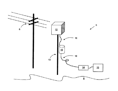
FIG 2 shows a system 5 including protection device 10 in accordance with one
embodiment of the invention. System 5 includes an antenna 12 in signal
communication
and electrical communication with the protection device 10 via first cable 16.
Thus, RF
signals as well as high voltage AC or DC currents pass from antenna 12 to
protection
3
CA 02768269 2012-02-16
247164-4
device 10. System 5 further includes a signal receiving device 14, which may
be a radio
device such as a receiver or a transceiver such as a WiFi or WiMax wireless
modem
among other types of receiving devices, or it could be testing equipment such
as a
spectrum analyzer used to measure RF signal strength. Protection device 10 is
inserted
into the path between signal receiving device 14 and antenna 12, typically
using first and
second cables 16 and 18 as shown in FIG 2. In some embodiments, cables 16, 18
may be
coaxial cables. RF signals propagate through protection device 10, however
high voltage
AC or DC currents are blocked owing to the separation between the two halves
of the
protection device. Protection device 10, which will be described in greater
detail below,
electrically insulates receiving device 14 from antenna 12. Receiving device
14 may
further be in signal communication with a computing device 15 such as, e.g., a
laptop
computer, used to analyze signals received.
In one embodiment, antenna 12 may be affixed to mast 13, used to position
antenna 12 to
conduct a site survey. Mast 13 may be made of fiberglass or other electrically
insulating
material. First cable 16 may have a length, for example, 1-2 meters, such that
when
antenna 12 is raised on mast 13, protection device 10 is out of reach of
personnel on the
ground, preventing them from harm due to high voltage present on cable 16 and
first
waveguide 20 should the antenna touch power lines 6.
Protection device 10 is illustrated in greater detail in FIG 3. As shown in
FIG 3,
protection device 10 includes first waveguide 20 in signal communication and
electrical
communication with antenna 12 (FIG 2) via first cable 16. Protection device 10
further
includes second waveguide 22, which is in signal communication with first
waveguide 20
and signal receiving device 14 (FIG 2) via second cable 18. First waveguide 20
and
second waveguide 22 are arranged in an end to end coaxial relationship facing
one
another, but are electrically insulated from one another. In the embodiment
depicted in
FIG 3, each of first and second waveguides 20, 22 are circular waveguides. In
other
embodiments, however, as in FIGS. 4-5, each of first and second waveguides 20,
22 may
be rectangular waveguides. In still further embodiments, other antenna
structures may be
used, such as radio frequency (RF) transformers or pairs of coupled coils.
4
CA 02768269 2012-02-16
247164-4
Regardless of the shape of first and second waveguides 20, 22, each waveguide
further
includes a connector 28, 30 for providing signal connectivity between
protection device
and first and second cables 16, 18, respectively. A first connector 28 is
disposed
between first waveguide 20 and antenna 12. As shown in FIG. 3, first connector
28
includes a first pin 32 inserted through a wall of first waveguide 20. A first
wire 38 is
connected to an end of the first pin 32 on an interior of waveguide 20 by,
e.g., soldering
or other means known in the art. First wire 38 extends from the end of first
pin 32 into an
interior of first waveguide 20. First cable 16 connects the opposite end of
first pin 32, on
an exterior of waveguide 20, with antenna 12. Second connector 30 is disposed
between
second waveguide 22 and signal receiving device 14 in a fashion similar to
first
connector 28. Second connector 30 includes second pin 34 inserted through a
wall of
second waveguide 22. A second wire 40 is connected to an end of the second pin
34 on
an interior of waveguide 22 by, e.g., soldering or other means known in the
art. Second
wire 40 extends from the end of second pin 34 into an interior of second
waveguide 22.
Second cable 18 connects the opposite end of second pin 34, on an exterior of
waveguide
22, with signal receiving device 14. As in the embodiments shown in FIGS. 3-4,
connectors 28, 30 may each be disposed on an axially extending face of
waveguides 20,
22 respectively. However, in other embodiments, such as the one shown in FIG 5
connectors 28, 30 may be located on end faces of waveguides 20, 22.
Referring again to FIG. 3, first waveguide 20 is physically isolated from
second
waveguide 22 by a distance 36 which may vary with the size of protection
device 10 and
the frequency of the RF signal being propagated therethrough. In one
embodiment which
may be used at frequencies including but not limited to the range of about 3.5
GHz to
about 4.0 GHz, distance 36 may be equal to approximately 1 mm. In other
embodiments
of protection device 10, in which the size of waveguides 20, 22 and other
parameters may
vary, distance 36 may be either more or less than 1 mm. Distance 36 represents
a balance
between quality of the RF signal passed through protection device 10 and the
amount of
protection provided from high voltage. As distance 36 increases, it may
introduce some
loss in the desired RF signal being coupled through protection device 10. As
distance 36
5
CA 02768269 2012-02-16
247164-4
decreases, distance 36 may not provide adequate insulation from high voltages.
Accordingly, distance 36 may vary with application. Some embodiments may
further
include insulating material 46 between waveguides 20, 22 to provide insulation
from high
voltages. The particular insulating material 46 may be chosen to withstand a
particular
voltage or range of voltages. For example, in an embodiment having a 1 mm
thick
insulating material 46 having an exemplary dielectric strength of 15 kV/mm,
insulating
material 46 would insulate against a 15,000 volt current. In one embodiment,
the
insulating material 46 may be a polyimide tape having a dielectric strength of
about, e.g.,
291 kV/mm. In other embodiments, materials such as, e.g., plastics having a
dielectric
strength of about 15 kV/mm to about 20 kV/mm, or polytetrafluoroethylene,
having a
dielectric strength of about 60 kV/mm, may be used as insulating material 46,
among
other suitable materials. The use of insulating material 46 allows for a
greater degree of
electrical isolation between waveguides 20, 22, and therefore greater
protection,
particularly where distance 36 is small.
Waveguides 20, 22 may be cast from, e.g., aluminum, brass, stainless steel,
and other
materials, and may each include a flange 42 to facilitate affixing one to the
other.
Waveguides 20, 22 may be affixed to one another using any conventional means
such as
nylon/insulated screws or bolts 44. In other embodiments, rather than separate
waveguides 20, 22, protection device 10 may be made from a single plastic
cavity with a
metallized coating at each end, and a void between the metallized ends
providing the
necessary electrical insulation. In such an embodiment, air, having a pressure-
dependent
dielectric strength of about 3 kV/mm, or other gas, takes the place of both
distance 36 and
insulating material 46.
Protection device 10 may be used over a variety of frequencies of RF signal.
In some
embodiments, the frequency of the RF signal transferred may be from about 1
GHz to
about 300 GHz. The size of waveguides 20, 22 may vary by application, relative
to the
desired frequency of the RF signal from antenna 12. More specifically, the
size of
waveguides 20, 22 is inversely proportional to the frequency of the RF signal
being
transferred. Therefore, lower frequencies will require larger waveguides 20,
22. In one
6
CA 02768269 2012-02-16
247164-4
embodiment, waveguides 20, 22 are circular waveguides, and a diameter of each
of the
first and the second waveguides is about 5.08 cm; a length of each of the
first and the
second waveguides is about 10.16 cm; and a frequency of an RF signal from
antenna 12
is about 3.5 GHz to about 4.0 GHz. This is only one possible embodiment,
however.
Referring to FIG 4, in another embodiment, by way of example only, waveguides
20, 22
are rectangular waveguides, and a length and width of each of the first and
the second
waveguides is about 5.8 cm and 2.9 cm respectively, exclusive of flange 42;
and a
frequency of a signal from antenna 12 is between about 3.3 GHz and about 4.9
GHz. As
noted, for use with a lower frequency RF signal, waveguides 20, 22 having a
larger
diameter and length may be used. The following waveguide sizes and frequencies
are
merely exemplary, and are not intended to be limiting in nature:
Frequency Band of operation Inner dimensions of waveguide
(GHz) (approximate) opening (cm) (approximate)
1.15-1.72 16.51 x 8.255
1.45-2.20 12.954 x 6.477
1.72-2.60 10.922 x 5.461
2.20-3.30 8.636
2.60-3.95 7.2136 x 3.4036
3.30-4.90 5.8166 x 2.9083
3.95-5.85 4.7549 x 2.2149
4.90-7.05 4.0386 x 2.0193
5.85-8.20 3.4849 x 1.5799
7.05 -10.00 2.8499 x 1.2624
8.20-12.40 2.286 x 1.0160
10.00 - 15.00 1.9050 x 0.9525
12.40 - 18.00 1.5799 x 0.7899
15.00 - 22.00 1.2954 x 0.6477
18.00 - 26.50 1.0668 x 0.4318
22.00 - 33.00 0.8636 x 0.4318
26.50 - 40.00 0.7112 x 0.3556
33.00 - 50.00 0.5690 x 0.2845
40.00 - 60.00 0.4775 x 0.2388
50.00 - 75.00 0.3759 x 0.1880
60.00 - 90.00 0.3099 x 0.1549
75.00 - 110.00 0.2540 x 0.1270
7
CA 02768269 2012-02-16
247164-4
90.00 -140.00 0.2032 x 0.1016
112.00 - 172.00 0.1651 x 0.0826
140.00 - 220.00 0.1295 x 0.0648
172.00 - 260.00 0.1092 x 0.0546
220.00 - 330.00 0.0864 x 0.0432
In addition to interrupting high voltage from flowing from antenna 12 to
signal receiving
device 14, protection device 10 may also be used to filter signals propagated
through the
network. Because of the relationship between size of waveguides 20, 22 and the
wavelength of the signal which they are designed to transfer, signals falling
outside a
given range of frequencies for a particular protection device 10 size will be
attenuated.
This has the advantage of reducing out of band noise and interference.
Protection device 10 is designed such that insertion into system 5 between
antenna 12 and
receiving device 14 results in almost no loss in RF signal strength, i.e.
typically less than
1 dB of loss is possible. Protection device also has a low voltage standing
wave ratio
(VSWR), i.e., typically 1.3:1. A VSWR of 1:0:1 represents an ideal device,
i.e. a device
having no effect on impedance match between antenna 12 and receiving device
14.
Devices having a VSWR of 1:5:1 are more typical.
As used herein, the terms "first," "second," and the like, do not denote any
order,
quantity, or importance, but rather are used to distinguish one element from
another, and
the terms "a" and " an" herein do not denote a limitation of quantity, but
rather denote the
presence of at least one of the referenced item. The modifier "about" used in
connection
with a quantity is inclusive of the stated value and has the meaning dictated
by the
context (e.g., includes the degree of error associated with measurement of the
particular
quantity). The suffix "(s)" as used herein is intended to include both the
singular and the
plural of the term that it modifies, thereby including one or more of that
term (e.g., the
metal(s) includes one or more metals). Ranges disclosed herein are inclusive
and
independently combinable (e.g., ranges of "up to about 25 mm, or, more
specifically,
about 5 mm to about 20 mm," is inclusive of the endpoints and all intermediate
values of
the ranges of "about 5 mm to about 25 mm," etc.).
8
CA 02768269 2012-02-16
247164-4
While various embodiments are described herein, it will be appreciated from
the
specification that various combinations of elements, variations or
improvements therein
may be made by those skilled in the art, and are within the scope of the
invention. In
addition, many modifications may be made to adapt a particular situation or
material to
the teachings of the invention without departing from essential scope thereof.
Therefore,
it is intended that the invention not be limited to the particular embodiment
disclosed as
the best mode contemplated for carrying out this invention, but that the
invention will
include all embodiments falling within the scope of the appended claims.
9