Note: Descriptions are shown in the official language in which they were submitted.
CA 02768790 2013-09-11
1
PRINTING APPARATUS, PRINTING MATERIAL CARTRIDGE, ADAPTOR
FOR PRINTING MATERIAL CONTAINER, AND CIRCUIT BOARD
CROSS-REFERENCE TO RELATED APPLICATIONS
[0001] The present application claims the priority based on Japanese Patent
Application
No. 2010-197316 filed on September 3, 2010.
BACKGROUND
Technical Field
[0002] This invention relates to a printing apparatus, a printing material
cartridge used for
the printing apparatus, an adaptor for a printing material container, and
circuit boards for
these components.
Related Art
[0003] In recent years, a cartridge equipped with a memory device that stores
information
pertaining to printing materials (such as the amount of remaining ink) is used
as a printing
material cartridge. Also, a technology to detect attachment conditions of the
printing
material cartridges has been used. For example, in JP-A-2009-274438,
attachment
conditions of cartridges are detected by sending signals different from those
for detecting
the amount of remaining ink to the remaining ink sensor installed in the ink
cartridge. In
conventional technologies, attachment conditions have been commonly detected
by the use
of one or two of many terminals on the cartridge.
[0004] However, even if the proper attachment of the cartridge is detected,
some other
terminals not used for the detection of attachment conditions may sometimes be
in poor
contact with the terminals of the printing apparatus. Especially when the
terminals for a
memory device are in poor contact, a problem arises that errors tend to occur
when data are
written and read to and from the memory device.
[0005] Meanwhile, known technologies for detecting attachment conditions of
CA 02768790 2012-02-07
2
ink cartridges include those described in JP -A-2002-198627 and
JP-A-2009-241591. According to these documents, the attachment detection
terminal on the cartridge side is grounded, while the attachment detection
terminal on the printing apparatus side is pulled up to a power supply voltage
via a resistance. If the attachment detection terminal on the cartridge side
is
in good contact with that on the printing apparatus side, the terminal on the
printing apparatus side bears a ground voltage, whereas it is applied with a
power supply voltage in case of non-contact. Therefore, attachment of the
cartridge can be detected by monitoring the voltage of the attachment
detection
terminal on the printing apparatus side. Detection of cartridge attachment is
also possible in a way opposite to that mentioned above, that is, by
connecting
the attachment detection terminal on the cartridge side to the power supply
voltage, and at the same time, pulling down the attachment detection terminal
on the printing apparatus side via a resistance. In general, cartridge
attachment can be detected by connecting the attachment detection terminal
on the cartridge side to a first fixed voltage, and connecting the attachment
detection terminal on the printing apparatus side to a second fixed voltage
via a
resistance. However, keeping the voltage of the attachment detection
terminal on the cartridge side constant may cause another problem. For
example, in a configuration where the attachment detection terminal on the
cartridge side is grounded, if the attachment detection terminal on the
printing
apparatus side bears a ground voltage from any cause, the system may
erroneously identify a non-attached cartridge as attached. This would cause a
problem of less reliability of attachment detection. Also, in a configuration
where the attachment detection terminal on the cartridge side is grounded, if
a
high voltage (e.g. voltage for operating a print head) is mistakenly applied
to
the attachment detection terminal, a problem may arise that a large current
flows through the attachment detection terminal to inflict damages to the
circuitry of the cartridge or the printing apparatus.
[0006] In addition, on a circuit board installed on a cartridge, increased
number of terminals or contact portions means a higher risk of poor contact at
CA 02768790 2012-02-07
3
one or more of them. Therefore, there has been a desire to reduce the number
of terminals and contact portions as much as possible.
[0007] The various problems mentioned above are not limited to ink cartridges
but also applicable to printing material cartridges containing other types of
printing materials (e.g. tonner). Moreover, the same problem existed with
liquid injection devices that inject different types of liquid other than the
above
printing materials and liquid containers (liquid storages) thereof. In
addition,
there have been similar problems with the detection of connection conditions
between the circuit board terminals used for printing cartridges or liquid
containers and the corresponding terminals on the apparatus side.
[0008] An object of the present invention is to provide a technology that
properly checks attachment conditions of cartridges or their circuit boards. A
second object of this invention is to provide a technology to properly
evaluate
whether the contact between terminals of a memory device for the cartridge or
those of the circuit board and the corresponding apparatus-side terminals is
enough or not. A third object of this invention is to provide a technology to
perform attachment detection without keeping the attachment detection
terminals of a cartridge or a circuit board for a cartridge at a fixed
voltage.
This invention does not need to have a configuration that achieves all of the
above objects, and may be implemented in a way in which to have a
configuration that achieves one of the above objects or other effects
described
later.
SUMMARY
[0009] (1) According to an aspect of the invention, there is provided a
circuit
board electrically connectable to a plurality of apparatus-side terminals of a
cartridge attachment unit of a printing apparatus. The circuit board
comprises: a memory device; a plurality of first terminals through which a
power source voltage and signals for operating the memory device are supplied
from the printing apparatus; and a plurality of second terminals to be used
for
detecting connection conditions between the plurality of apparatus-side
CA 02768790 2012-02-07
4
terminals and the circuit board. The plurality of first terminals have a
plurality of first contact portions that get in contact with corresponding
apparatus-side terminals. The plurality of second terminals have a plurality
of second contact portions that get in contact with corresponding
apparatus-side terminals. The plurality of first and second contact portions
are arranged so as to form a first row and a second row. Four contact portions
among the plurality of second contact portions are placed at both ends of the
first and second rows, respectively. According to this configuration,
connection
conditions or attachment conditions of the circuit board may be properly
judged
because four contact portions for the detection of the connection conditions
of
the circuit board are placed at both ends of the first and second rows.
[0010] (2) As to the circuit board, the plurality of first contact portions
may
be placed within a first area. The four contact portions among the plurality
of
second contact portions may be placed outside the first area and are arranged
at positions corresponding to four corners of a second area of a quadrangular
shape encompassing the first area. The second area may have a trapezoid
shape having a first base corresponding to the first row shorter than a second
base corresponding to the second row. According to this configuration, since
four second contact portions are placed at both ends of the first bottom base
and
the second bottom base of the second area of a trapezoidal shape, it is
possible
to reduce the severity of the problem, as opposed to the situation where the
second area is of a rectangular shape, that the contact condition at the
second
contact portions is poor even if the contact conditions at the plurality of
first
contact portions are good, when the circuit board is tilted from the normal
position.
[0011] (3) As to the circuit board, among the four contact portions of the
plurality of second contact portions, two contact portions placed at both ends
of
the first row may be connected with each other and neither of them are
connected to a fixed voltage, and two contact portions placed at both ends of
the
second row may be connectable to an electric device. According to this
configuration, it is possible to use two contact portions placed at both ends
of
CA 02768790 2012-02-07
the second row for both contact detection and sending/receiving of signals to
and from the electric device. Also, since neither of two contact portions
placed
at both ends of the first row is connected at a fixed voltage, it is possible
to
prevent a problem that if they are grounded, for example, a terminal of the
5 circuit board of poor contact is misjudged to be in a good contact when
the
terminal on the printing apparatus side bears a ground voltage from any cause.
Also, when a high voltage (e.g. voltage for driving a print head) is
erroneously
applied to the contact portions for connection detection, it is possible to
prevent
a problem of having a large current flow through the contact portions to
damage the circuitry of the circuit board or the printing apparatus.
[0012] (4) As to the circuit board, a contact portion of a ground terminal for
the memory device may be placed at the center of the second row. According to
this configuration, it is possible to prevent the plurality of second contact
portions from being connected to a ground terminal due to foreign matters such
as dirt or dust.
[0013] (5) As to the circuit board, during detection of connection conditions
between the plurality of apparatus-side terminals and the circuit board, a
voltage which is no higher than a first power supply voltage supplied to a
power
terminal for the memory device may be applied to the two contact portions at
both ends of the first row, and a voltage which is no higher than a second
power
supply voltage for driving a print head of the printing apparatus and higher
than the first power supply voltage may be applied to the two contact portions
at both ends of the second row. According to this configuration, since
detection
of connection conditions is performed with a lower voltage at two contact
portions at both ends of the first row than at two contact portions at both
ends
of the second row, time required for charging the wiring can be reduced
compared to the case of detecting with a higher voltage, thus completing the
detection in shorter time. Also, since detection of connection conditions is
performed with a higher voltage at two contact portions at both ends of the
second row than at those at both ends of the first row, it is possible to
enhance
the detection accuracy compared to the case of detecting with a lower voltage.
CA 02768790 2012-02-07
6
[0014] (6) As to the circuit board, during detection of connection conditions
between the plurality of apparatus-side terminals and the circuit board, a
first
attachment inspection signal is inputted, as a first pulse signal, to one of
the
two contact portions at both ends of the first row, and a first attachment
response signal may be outputted from the other of the two contact portions in
response to the first attachment inspection signal, and a first voltage no
more
than the second power supply voltage and higher than the first power supply
voltage may be applied to one of the two contact portions at both ends of the
second row, and a voltage lower than the first voltage and higher than the
first
power supply voltage is outputted from the other of the two contact portions
at
both ends of the row. According to this configuration, two contact portions at
both ends of the first row are used for attachment detection (contact
detection)
as a first pair, whereas two contact portions at both ends of the second row
are
used for the same as a second pair. Therefore, it is possible to perform
attachment detection (contact detection) without providing extra contact
portions other than those four contact portions, thus reducing the number of
contact portions on the circuit board.
[0015] (7) As to the circuit board, the two contact portions at both ends of
the
first row may be also used for detecting an overvoltage applied to the two
contact portions at both ends of the first row, and a high level voltage of
the first
attachment inspection signal may be set lower than the overvoltage.
According to this configuration, since two contact portions at both ends of
the
first row can be used for both contact detection and overvoltage detection, it
is
possible to reduce the number of contact portions on the circuit board. Also,
since the high level voltage of the first attachment detection signal is set
at a
lower voltage than the overvoltage, it is possible to prevent a problem of
misjudging it as overvoltage in the process of attachment detection (contact
detection).
[0016] (8) As to the circuit board, two contact portions placed at both ends
of
the second row may be connectable to an electric device, and the electric
device
may be a resistance element installed in the circuit board. According to this
CA 02768790 2012-02-07
7
configuration, it is possible to evaluate in high precision whether the
circuit
boards are properly installed by measuring the current or voltage
corresponding to the voltage applied to the contact portions at both ends of
the
second row.
[0017] (9) As to the circuit board, during detection of connection conditions
between the plurality of apparatus-side terminals and the circuit board, a
first
attachment inspection signal may be inputted, as a first pulse signal, to one
of
the two contact portions at both ends of the first row, and a first attachment
response signal may be outputted from the other of the two contact portions in
response to the first attachment inspection signal; and a second attachment
inspection signal may be inputted, as a second pulse signal, to one of the two
contact portions at both ends of the second row, and a second attachment
response signal may be outputted from the other of the two contact portions in
response to the second attachment inspection signal. According to this
configuration, contact portions at both ends of the first row are used for
attachment detection (contact detection) as a first pair, while those at both
ends
of the second row are used for the same as a second pair. This makes it
possible to perform attachment detection (or contact detection) without
providing extra contact portions other than the above four. Also, according to
this configuration, since the attachment detection (or contact detection)
pertaining to the first and second pairs is performed by the use of the first
and
second attachment inspection signals that are different from each other, it is
always possible to evaluate properly which pair of contact portions are in
poor
attachment (or contact) conditions.
[0018] (10) As to the circuit board, a rise timing of the second attachment
inspection signal from a low to a high level may be different from a rise
timing
of the first attachment inspection signal from a low to a high level.
According
to this configuration, since the rise timings of the first and second
attachment
inspection signals are different from each other, it is always possible to
evaluate properly which of the first and second pairs of contact portions are
in
poor attachment (or contact) conditions.
CA 02768790 2012-03-21
8
[00191(11)
As to the circuit board, the two contact portions at both
ends of the first row may be also used for detecting an overvoltage
applied to the two contact portions at both ends of the first row, and
a high level voltage of the first attachment inspection signal may be
set lower than the overvoltage.
According to this configuration,
since two contact portions at both ends of the first row can be used
for detecting both contact conditions and overvoltage, it is possible
to reduce the number of contact portions on the circuit board. Also,
the high level voltage of the first attachment inspection signal is
set at a lower voltage than the overvoltage, which prevents the
condition from being misjudged as overvoltage in the process of
attachment (or contact) detection.
[00201(12)
As to the circuit board, two contact portions placed at
both ends of the second row may be connectable to an electric device,
and the electric device may be a sensor to be used for detecting a
remaining amount of printing material within a printing material
cartridge attached to the cartridge attachment unit. According to
this configuration, since two contact portions at both ends of the
second row can be used for detecting both contact conditions and the
remaining amount of the printing material, it is possible to reduce
the number of contact portions on the circuit board.
[00211(13)
As to the circuit board, the plurality of first terminals
may include a ground terminal for supplying a ground voltage from
the printing apparatus to the memory device, a power supply
terminal for supplying power at a different voltage than the ground
voltage from the printing apparatus to the memory device, a clock
terminal for supplying clock signals from the printing apparatus to
the memory device, a reset terminal for supplying reset signals
from the printing apparatus to the memory device, and a data
terminal for supplying data signals from the printing apparatus to
the memory device.
Two of the first contact portions may be
placed in the first row, and three of the first contact portions are
placed in the second row. According to this configuration, it is
possible to surely detect contact conditions at the contact portion of
each terminal for the memory device, whether they are good or poor,
by the four contact portions surrounding them.
CA 02768790 2012-02-07
9
[0022] (14) As to the circuit board, a distance between two contact portions
which are placed at both ends among the first and second contact portions
existing in the first row may be longer than a distance between two contact
portions which are placed at both ends among the first contact portions
existing
in the second row.
[0023] (15) As to the circuit board, the circuit board may be to be attached
to
a cartridge attachment unit of the printing apparatus that comprises a print
head and the cartridge attachment unit.
[0024] (16) According to another aspect of the invention, there is provided a
printing material cartridge attachable to a cartridge attachment unit of a
printing apparatus having a plurality of apparatus-side terminals. The
printing material cartridge comprises: a memory device; a plurality of first
terminals through which a power source voltage and signals for operating the
memory device are supplied from the printing apparatus; and a plurality of
second terminals to be used for detecting attachment conditions of the
printing
material cartridge in the cartridge attachment unit. The plurality of first
terminals have a plurality of first contact portions that get in contact with
corresponding apparatus-side terminals when the printing material container
is properly attached to the cartridge attachment unit. The plurality of second
terminals have a plurality of second contact portions that get in contact with
corresponding apparatus-side terminals when the printing material container
is properly attached to the cartridge attachment unit. The plurality of first
and second contact portions are arranged so as to form a first row and a
second
row. Four contact portions among the plurality of second contact portions are
placed at both ends of the first and second rows, respectively. According to
this configuration, attachment conditions of the printing material container
may be properly judged because four contact portions of the plurality of
second
terminals are placed at both ends of the first and second rows.
[0025] (17) According to an aspect of the invention, there is provided a
printing material container adapter to which a printing material container is
to
be attached, the adapter being attachable to a cartridge attachment unit of a
CA 02768790 2012-02-07
printing apparatus having a plurality of apparatus-side terminals. The
adapter comprises: a memory device; a plurality of first terminals through
which a power source voltage and signals for operating the memory device are
supplied from the printing apparatus; and a plurality of second terminals to
be
5 used for detecting attachment conditions of the printing material container
adapter in the cartridge attachment unit. The plurality of first terminals
have
a plurality of first contact portions that get in contact with corresponding
apparatus-side terminals when the printing material container adapter is
properly attached to the cartridge attachment unit. The plurality of second
10 terminals have a plurality of second contact portions that get in
contact with
corresponding apparatus-side terminals when the printing material container
adapter is properly attached to the cartridge attachment unit. The plurality
of
first and second contact portions are arranged so as to form a first row and a
second row. Four contact portions among the plurality of second contact
portions are placed at both ends of the first and second rows, respectively.
According to this configuration, attachment conditions of the printing
material
container adapter may be properly judged because four contact portions of the
plurality of second terminals are placed at both ends of the first and second
rows.
[0026] (18) According to still another aspect of the invention, there is
provided a printing apparatus. The printing apparatus comprises: a cartridge
attachment unit to which a printing material cartridge is attached; a printing
material cartridge attachable to the cartridge attachment unit; an attachment
detection circuit for detecting attachment conditions of the printing material
cartridge; and apparatus-side terminals. The printing material cartridge
comprises: a memory device; a plurality of first terminals through which a
power source voltage and signals for operating the memory device are supplied
from the printing apparatus; and a plurality of second terminals to be used
for
detecting attachment conditions of the printing material cartridge in the
cartridge attachment unit. The plurality of first terminals have a plurality
of
first contact portions that get in contact with corresponding apparatus-side
CA 02768790 2013-09-11
11
terminals when the printing material container is properly attached to the
cartridge
attachment unit. The plurality of second terminals have a plurality of second
contact
portions that get in contact with corresponding apparatus-side terminals when
the printing
material container is properly attached to the cartridge attachment unit. The
plurality of
first and second contact portions are arranged so as to form a first row and a
second row.
Four contact portions among the plurality of second contact portions are
placed at both
ends of the first and second rows, respectively. According to this
configuration,
attachment conditions of the printing material container may be properly
judged because
four contact portions of the plurality of second terminals are placed at both
ends of the first
and second rows.
[0026a] In a
further aspect, the present invention provides a circuit board
electrically connectable to a plurality of apparatus-side terminals of a
cartridge attachment
unit of a printing apparatus, the printing apparatus having an attachment
detection circuit
and a memory control circuit, the circuit board comprising: a memory device; a
plurality of
first terminals connected to the memory device, wherein the plurality of first
terminals are
connected to the memory control circuit when the circuit board is connected to
the
cartridge attachment unit so that a power source voltage and signals for
operating the
memory device are supplied through the first terminals from the printing
apparatus; and a
plurality of second terminals connected to the attachment detection circuit
when the circuit
board is connected to the cartridge attachment unit for detecting connection
status of the
plurality of apparatus-side terminals with the circuit board, wherein the
plurality of first
terminals respectively have a first contact portion for contacting a
corresponding
apparatus-side terminal among the plurality of apparatus-side terminals, the
plurality of
second terminals respectively have a second contact portion for contacting a
corresponding
apparatus-side terminal among the plurality of apparatus-side terminals, the
plurality of
first and second contact portions are arranged so as to form a first row and a
second row,
CA 02768790 2013-09-11
11a
and four contact portions of the plurality of second contact portions are
disposed
respectively at the ends of the first and second rows.
[0026b] In a further aspect, the present invention provides a printing
material
cartridge attachable to a cartridge attachment unit of a printing apparatus
having a plurality
of apparatus-side terminals, an attachment detection circuit and a memory
control circuit
comprising: a memory device; a plurality of first terminals connected to the
memory
device, wherein the plurality of first terminals are connected to the memory
control circuit
when the printing material container is attached to the cartridge attachment
unit so that a
power source voltage and signals for operating the memory device are supplied
through the
first terminals from the printing apparatus; and a plurality of second
terminals connected to
the attachment detection circuit when the printing material container is
attached to the
cartridge attachment unit for detecting attachment status of the printing
material cartridge
in the cartridge attachment unit, wherein the plurality of first terminals
respectively have a
first contact portion for contacting a corresponding apparatus-side terminal
among the
plurality of apparatus-side terminals when the printing material container is
attached to the
cartridge attachment unit, the plurality of second terminals respectively have
a second
contact portion for contacting a corresponding apparatus-side terminal among
the plurality
of apparatus-side terminals when the printing material container is attached
to the cartridge
attachment unit, the plurality of first and second contact portions are
arranged so as to
form a first row and a second row, and four contact portions of the plurality
of second
contact portions are disposed respectively at the ends of the first and second
rows.
[0026c] In a still further aspect, the present invention provides a
printing material
container adapter to which a printing material container is to be attached,
the adapter being
attachable to a cartridge attachment unit of a printing apparatus, the
printing apparatus
having an attachment detection circuit and a memory control circuit, the
adapter
comprising: a memory device; a plurality of first terminals connected to the
memory
CA 02768790 2013-09-11
llb
device, wherein the plurality of first terminals are connected to the memory
control circuit
when the circuit board is connected to the cartridge attachment unit so that a
power source
voltage and signals for operating the memory device are supplied through the
first
terminals from the printing apparatus; and a plurality of second terminals
connected to the
attachment detection circuit when the circuit board is connected to the
cartridge attachment
unit for detecting attachment status of the printing material container
adapter in the
cartridge attachment unit, wherein the plurality of first terminals
respectively have a first
contact portion for contacting a corresponding apparatus-side terminal among
the plurality
of apparatus-side terminals when the printing material container adapter is
attached to the
cartridge attachment unit, the plurality of second terminals respectively have
a second
contact portion for contacting a corresponding apparatus-side terminal among
the plurality
of apparatus-side terminals when the printing material container adapter is
attached to the
cartridge attachment unit, the plurality of first and second contact portions
are arranged so
as to form a first row and a second row, and four contact portions of the
plurality of second
contact portions are disposed respectively at the ends of the first and second
rows.
[0026d] In a
further aspect, the present invention provides a printing apparatus
comprising: a cartridge attachment unit; a printing material cartridge
attached to the
cartridge attachment unit; a memory control circuit; an attachment detection
circuit for
detecting attachment conditions of the printing material cartridge; and
apparatus-side
terminals, wherein the printing material cartridge comprising: a memory
device; a plurality
of first terminals connected to the memory device, wherein the plurality of
first terminals
are connected to the memory control circuit when the printing material
container is
attached to the cartridge attachment unit so that a power source voltage and
signals for
operating the memory device are supplied through the first terminals from the
printing
apparatus; and a plurality of second terminals connected to the attachment
detection circuit
when the printing material container is attached to the cartridge attachment
unit for
CA 02768790 2013-09-11
lic
detecting attachment status of the printing material cartridge in the
cartridge attachment
unit wherein the plurality of first terminals respectively have a first
contact portion for
contacting a corresponding apparatus-side terminal among the plurality of
apparatus-side
terminals when the printing material container is attached to the cartridge
attachment unit,
the plurality of second terminals respectively have a second contact portion
for contacting
a corresponding apparatus-side terminal among the plurality of apparatus-side
terminals
when the printing material container is attached to the cartridge attachment
unit, the
plurality of first and second contact portions are arranged so as to form a
first row and a
second row, and four contact portions of the plurality of second contact
portions are
disposed respectively at the ends of the first and second rows.
[0027] (19) In the above printing apparatus, N pieces of printing material
cartridges
may be attachable to the cartridge attachment unit where N is an integer no
less than 2.
Two contact portions placed at both ends of the first row in respective ones
of the N pieces
of printing material cartridges may be connected in series according to an
arrangement
order of the N pieces of printing material cartridges in the cartridge
attachment unit via
plural device-side terminals installed in the cartridge attachment unit so as
to form a wiring
route, and both ends of the wiring route is connected to the attachment
detection circuit.
Two contact portions placed at both ends of the second row in respective ones
of the N
pieces of printing material cartridges may be connected individually to the
attachment
detection circuit per each printing material cartridge. The attachment
detection circuit
may judge: (i) whether all the N pieces of printing material cartridges are
attached to the
cartridge attachment unit by detecting connection conditions of the wiring
route, and (ii)
whether individual printing material cartridges are attached by detecting
connection
conditions of the two contact portions placed at both ends of the second row
in each
printing material cartridge. According to this configuration, the first
attachment detection
process using the two contact portions at both ends of the first row and the
second
attachment detection process using the two contact portions at both ends of
the second row may be
CA 02768790 2012-02-07
12
respectively performed. Thus, if the proper attachment conditions are
confirmed by these two kinds of attachment detection processes, it is
confirmed
that the memory device terminals for each cartridge are also in good contact
conditions.
[0028] This invention may also be realized as the following application
examples.
[0029]
<Application example 1>
A printing material cartridge attachable to a cartridge attachment unit
having a plurality of apparatus-side terminals of a printing apparatus,
comprising: a memory device, a plurality of first terminals connected to the
memory device, and a plurality of second terminals to be used for detecting
attachment conditions of the printing material cartridge in the cartridge
attachment unit; the plurality of first terminals have respective first
contact
portions that get in contact with corresponding apparatus-side terminals when
the printing material cartridge is properly attached to the cartridge
attachment
unit; the plurality of second terminals have respective second contact
portions
that get in contact with corresponding apparatus-side terminals when the
printing material cartridge is properly attached to the cartridge attachment
unit; the first contact portions are arranged within a first area, the second
contact portions are arranged outside the first area; and the second contact
portions include four contact portions located at four corners of a
quadrangular
second area encompassing the first area.
According to this configuration, all the first terminals connected to the
memory device may be confirmed to be in good contact with the corresponding
apparatus-side terminals by checking the contact conditions between the
plurality of second contact portions, which are used for detecting attachment
conditions of the printing material cartridges, and the corresponding
apparatus-side terminals.
[0030]
Application example 2>
CA 02768790 2012-02-07
13
The printing material cartridge described in Application example 1,
wherein the first and second contact portions are arranged so as to form a
first
row and a second row, and the four contact portions among the second contact
portions are arranged at both ends of the first row and second row
respectively.
According to this configuration, attachment conditions of the printing
material cartridge may be checked properly because the second contact portions
for detecting attachment conditions are provided at both ends of the first row
and the second row.
[0031]
<Application example 3>
The printing material cartridge described in Application example 2,
wherein among the four contact portions of the second contact portions, two
contact portions arranged at both ends of the first row are connected with
each
other via wiring, and an electric device installed in the printing material
cartridge is connected between the two contact portions arranged at both ends
of the second row.
According to this configuration, the two contact portions placed on both
ends of the second row may be used for both detecting the attachment
conditions and for sending and receiving signals to and from the electric
device.
[0032]
<Application example 4>
The printing material cartridge described in Application example 3,
wherein, the electric device is a sensor used for detecting a remaining amount
of the printing material within the printing material cartridge.
[0033]
<Application example 5>
The printing material cartridge described in Application example 3,
wherein, the electric device is a resistance element.
[0034]
<Application example 6>
The printing material cartridge described in one of Application
CA 02768790 2012-02-07
14
examples 2-5, wherein the printing apparatus further comprises a print head
for discharging printing material, and the two contact portions arranged at
both ends of the first row are supplied with a same voltage as a first power
voltage for driving the memory device or a voltage generated from the first
power voltage, and the two contact portions arranged at both ends of the
second
row are supplied with a same voltage as a second power voltage for driving the
print head or a voltage generated from the second power voltage.
According to this configuration, there is no need for providing a special
power source to detect attachment conditions because the attachment detection
is possible by the use of the first power-supply voltage for driving the
memory
device and the second power-supply voltage for driving the print head.
[0035]
Application example 7>
An adaptor for a printing material container attachable to a cartridge
attachment unit having a plurality of apparatus-side terminals of a printing
apparatus, comprising: a memory device, a plurality of first terminals
connected to the memory device, and a plurality of second terminals to be used
for detecting attachment conditions of the adaptor in the cartridge attachment
unit; the plurality of first terminals have respective first contact portions
that
get in contact with corresponding apparatus-side terminals when the adaptor is
properly attached to the cartridge attachment unit; the plurality of second
terminals have respective second contact portions that get in contact with
corresponding apparatus-side terminals when the adaptor is properly attached
to the cartridge attachment unit; the first contact portions are arranged
within
a first area; the second contact portions are arranged outside the first area;
and
the second contact portions include four contact portions located at four
corners
of a quadrangular second area encompassing the first area.
According to this configuration, all the first terminals connected to the
memory device may be confirmed to be in good contact with the corresponding
apparatus-side terminals by checking the contact conditions between the
plurality of second contact portions, which are used for detecting attachment
CA 02768790 2012-02-07
conditions of the adaptor, and the corresponding apparatus-side terminals.
[0036]
<Application example 8>
A circuit board electrically connectable to a plurality of apparatus-side
5 terminals in a cartridge attachment unit of a printing apparatus,
comprising: a
memory device, a plurality of first terminals connected to the memory device,
and a plurality of second terminals to be used for detecting attachment
conditions of the circuit board in the cartridge attachment unit; the
plurality of
first terminals have respective first contact portions that get in contact
with
10 corresponding apparatus-side terminals; the plurality of second
terminals have
respective second contact portions that get in contact with corresponding
apparatus-side terminals; the first contact portions are arranged within a
first
area; the second contact portions are arranged outside the first area, and the
second contact portions include four contact portions located at four corners
of a
15 quadrangular second area encompassing the first area.
According to this configuration, all the first terminals connected to the
memory device may be confirmed to be in good contact with the corresponding
apparatus-side terminals by checking the contact conditions between the
plurality of second contact portions, which are used for detecting attachment
conditions of the circuit board, and the corresponding apparatus-side
terminals.
[0037]
<Application example 9>
A printing apparatus comprising a cartridge attachment unit to which a
printing material cartridge is attached, a printing material cartridge that is
attachable to and detachable from the cartridge attachment unit, an
attachment detection circuit that detects attachment conditions of the
printing
material cartridge, and apparatus-side terminals; the printing material
cartridge comprises: a memory device, a plurality of first terminals connected
to the memory device, and a plurality of second terminals to be used for
detecting attachment conditions of the printing material cartridge in the
cartridge attachment unit; the plurality of first terminals have respective
first
CA 02768790 2012-02-07
16
contact portions that get in contact with corresponding apparatus-side
terminals when the printing material cartridge is properly attached to the
cartridge attachment unit; the plurality of second terminals have respective
second contact portions that get in contact with corresponding apparatus-side
terminals when the printing material cartridge is properly attached to the
cartridge attachment unit; the first contact portions are arranged within a
first
area; the second contact portions are arranged outside the first area, and the
second contact portions include four contact portions located at four corners
of a
quadrangular second area encompassing the first area.
According to this configuration, all the first terminals connected to the
memory device may be confirmed to be in good contact with the corresponding
apparatus-side terminals by checking the contact conditions between the
plurality of second contact portions, which are used for detecting attachment
conditions of the printing material cartridges, and the corresponding
apparatus-side terminals.
[0038] This invention may be embodied in various forms, for example, in a
form of a printing material cartridge, a printing material cartridge set
composed of plural kinds of printing material cartridges, a cartridge adapter,
a
cartridge adapter set composed of plural kinds of cartridge adapters, a
circuit
board, a printing apparatus, a liquid injection device, a printing material
supply system equipped with a printing apparatus and cartridges, a liquid
supply system equipped with a liquid injection device and cartridges, and a
method for detecting attachment conditions of the cartridges or circuit
boards.
BRIEF DESCRIPTION OF THE DRAWINGS
[0039]
Fig. 1 is a perspective view showing a configuration of the printing
apparatus according to an embodiment of this invention.
Figs. 2A and 2B are perspective views showing a configuration of an ink
cartridge.
Figs. 3A-3C show configurations of the circuit boards according to the
CA 02768790 2012-02-07
17
first embodiment.
Figs. 4A-4C shows configuration of the cartridge attachment unit.
Figs. 5A-5C show an ink cartridge attached within its housing.
Fig. 6 is a block diagram showing an electrical configuration of the ink
cartridge's circuit board and the printing apparatus according to the first
embodiment.
Fig. 7 shows a condition of connection between the circuit board and the
attachment detection circuit according to the first embodiment.
Fig. 8 shows the circuit board configuration according to the second
embodiment.
Fig. 9 is a block diagram showing an electrical configuration of the ink
cartridge's circuit board and the printing apparatus according to the second
embodiment.
Fig. 10 shows the internal configuration of the
sensor-related-processing circuit according to the second embodiment.
Fig. 11 is a block diagram showing the condition of contact between the
contact detection unit as well as liquid volume detection unit and the
cartridge
sensor.
Fig. 12 is a timing chart showing various signals used for the
attachment detection process.
Figs. 13A and 13B are timing charts showing typical signal waveforms
in case of poor contact.
Figs. 14A and 14B are timing charts showing typical signal waveforms
when the overvoltage detection terminals and the sensor terminals are in a
leaking condition.
Figs. 15A-15C show the conditions of contact among the circuit board,
contact detection unit, detection pulse generator, and non-attached condition
detection unit.
Figs. 16A and 16B are block diagrams showing configuration examples
of the leak detection unit placed within the non-attached condition detection
unit.
CA 02768790 2012-02-07
18
Fig. 17 is a timing chart showing attachment detection processes of four
cartridges.
Fig. 18 is a timing chart of a liquid volume detection process.
Figs. 19A and 19B are timing charts showing other examples of signals
used for the attachment detection processes.
Fig. 20 shows a configuration of the circuit board according to the third
embodiment.
Fig. 21 is a block diagram showing an electrical configuration of the ink
cartridge and printing apparatus according to the third embodiment.
Fig. 22 shows an internal configuration of the cartridge detection circuit
according to the third embodiment.
Figs. 23A-23D show details of the cartridge's attachment detection
process according to the third embodiment.
Fig. 24 shows an internal configuration of the individual-attachment
current detection unit according to the third embodiment.
Fig. 25 is a flow chart showing an overall procedure of the attachment
detection process according to the third embodiment.
Figs. 26A and 26B show a configuration of the individual-attachment
current detection unit according to the fourth embodiment.
Fig. 27 is a perspective view showing a configuration of the printing
apparatus according to another embodiment.
Fig. 28 is a perspective view showing a configuration of the ink
cartridge according to another embodiment.
Fig. 29 is a perspective view of the contact mechanism installed within
the cartridge attachment unit.
Fig. 30 is a section of a main portion to which the ink cartridge is
attached within the cartridge attachment unit.
Figs. 31A-31C show how the apparatus-side terminals get in contact
with the circuit board terminals when the cartridge is attached.
Figs. 32A and 32B show how the front end of the cartridge is engaged
followed by the rear end.
CA 02768790 2012-02-07
19
Figs. 33A-33G show the circuit board configurations according to
another embodiment.
Figs. 34A-34C show the circuit board configurations according to
another embodiment.
Figs. 35A-35C show the circuit board configurations according to
another embodiment.
Figs. 36A-36C show the circuit board configurations according to
another embodiment.
Fig. 37 shows the circuit board configuration according to another
embodiment.
Figs. 38A and 38B show the common circuit board configuration for
other embodiments.
Figs. 39A-39C show configurations of the color-by-color independent
cartridges, integrated multi-color cartridge compatible therewith, and their
common circuit board.
Fig. 40 shows a circuit configuration of the printing apparatus fit for the
cartridge in Fig. 39B.
Fig. 41 shows the conditions of contact between the cartridge detection
circuit and the common circuit board.
Figs. 42A and 42B are perspective views showing a configuration of the
ink cartridge according to another
embodiment.
Fig. 43 is a perspective views showing a configuration of the ink
cartridge according to another
embodiment.
Fig. 44 is a perspective views showing a configuration of the ink
cartridge according to another
embodiment.
Fig. 45 is a perspective views showing a configuration of the ink
cartridge according to another
embodiment.
CA 02768790 2012-02-07
Fig. 46 shows a variation example of the circuit for the
individual-attachment current detection unit.
DESCRIPTION OF EXEMPLARY EMBODIMENTS
5 [0040]
A. First embodiment:
Fig. 1 is a perspective view showing a configuration of the printing
apparatus according to the first embodiment of this invention. A printing
apparatus 1000 includes a cartridge attachment unit 1100 to which ink
10 cartridges are attached, an open-close cover 1200 and an operation unit
1300.
This printing apparatus 1000 is a large format inkjet printer that prints on
large-size paper (e.g. A2-A0 sizes) such as posters. The cartridge attachment
unit 1100 is also called a "cartridge holder" or simply a "holder." In the
example
shown in Fig. 1, four ink cartridges of black, yellow, magenta and cyan, for
15 example, may be attached individually to the cartridge attachment unit
1100.
As ink cartridges to be attached to the cartridge attachment unit 1100, any
other plural types of ink cartridges may be used. Fig. 1 shows X, Y and Z axes
that are at right angles to each other for the sake of explanation. The +X
direction is the direction in which an ink cartridge 100 is inserted into the
20 cartridge attachment unit 1100 (hereinafter called "insertion direction" or
"attachment direction"). The cover 1200 is provided to the cartridge
attachment unit 1100 in an open-close manner. The cover 1200 may be
omitted. The operation unit 1300 is an input device by which the user enters
various commands and settings, and is equipped with a display to give various
messages to the user. This printing apparatus 1000 is provided with a print
head, a main scanning drive mechanism and a sub-scanning drive mechanism
for scanning the print head, and a head driving mechanism that ejects ink by
driving the print head, which are not shown in the figure. This type of
printing apparatus, like the printing apparatus 1000, is called "off-carriage
type" where a cartridge to be replaced by the user is attached to the
cartridge
attachment unit which is placed at a location other than the carriage of the
CA 02768790 2012-02-07
21
printer head.
[0041] Figs. 2A and 2B show a perspective view of the ink cartridge 100. The
X, Y and Z axes in Figs. 2A and 2B correspond to those in Fig. 1. An ink
cartridge may be simply called a "cartridge." This cartridge 100 is in an
approximate shape of a flat cuboid, having its dimensions in three directions
L
L2 and L3, of which the length Ll in insertion direction is the largest, the
width
L2 is the smallest, and the height L3 falls in between. However, depending on
the type of printing apparatus, some cartridges have smaller length Ll than
the height L3.
[0042] The cartridge 100 comprises a front surface (first surface) Sf, a rear
surface (second surface) Sr, a top surface (third surface) St, a bottom
surface
(fourth surface) Sb, as well as two side surfaces Sc and Sd (fifth and sixth
surfaces). The front surface Sf is a plane located at the front end in the
insertion direction X. The front surface Sf and rear surface Sr are the
smallest
among the six planes and are opposing each other. Each of the front surface Sf
and rear surface Sr intersects with the top surface St, bottom surface Sb, and
the two side surfaces Sc and Sd. Under the condition where the cartridge 100
is attached to the cartridge attachment unit 1100, the top surface St is
located
at the top in the vertical direction, while the bottom surface Sb is located
at the
bottom in the same direction. The two side surfaces Sc and Sd are the largest
among the six planes, and are opposing each other. In the cartridge 100, an
ink chamber 120 (also called an "ink bag") made of a flexible material is
installed. Since the ink chamber 120 is formed with a flexible material, it
shrinks as ink is consumed, mainly reducing its thickness (width in
Y- direction) .
[0043] On the front surface, two positioning holes 131 and 132 and an ink
supply outlet 110 are provided. The two positioning holes 131 and 132 are
used for positioning where the cartridge is attached. The ink supply outlet
110
is connected to an ink supply tube of the cartridge attachment unit 1100 to
supply ink from the cartridge 100 to the printing apparatus 1000. On the top
surface St, a circuit board 200 is provided. In the example of Figs. 2A and
2B,
CA 02768790 2012-02-07
22
the circuit board 200 is fixed at the edge of the top surface St (at the
farthest
end of the insertion direction X). However, the circuit board 200 may be
placed at a location away from the edge of the top surface St, or even at a
location other than the top surface St. The circuit board 200 is equipped with
a non-volatile storage element used for storing information on ink. The
circuit
board 200 may be simply called the "board." The bottom surface Sb has a
stopper groove 140 used for fixing the cartridge 100 at the attachment
location.
The first side surface Sc and the second side surface Sd are opposing each
other
intersecting with the front surface Sf, top surface St, rear surface Sr and
bottom surface Sb. At the location where the second side surface Sd intersects
with the front surface Sf, a comb joint 134 is placed. This comb joint 134,
together with another comb joint of the cartridge attachment unit 1100, is
used
for preventing the cartridge from being erroneously attached.
[0044] The cartridge 100 is for large format inkjet printers. The cartridge
100
has dimensions larger than those of small format inkjet printers for
individual
users, and more capacity to contain ink. For example, the cartridge's length
L1 is no less than 100mm in case of large format inkjet printers, whereas it
is
no more than 70mm in case of small format inkjet printers. Also, the amount
of ink in full quantities is 17m1 or more (typically 100m1 or more) in case of
cartridges for large format inkjet printers, whereas it is 15m1 or less in
cartridges for small format inkjet printers. In many cases, cartridges for
large
format inkjet printers are mechanically engaged with the cartridge attachment
unit at their front surface (frontend plane in the insertion direction),
whereas
those for small format inkjet printers are mechanically engaged with the
attachment unit at their bottom surface. Cartridges for large format inkjet
printers tend to have more contact failures at the terminals of the circuit
board
200 than those for small format inkjet printer, caused by the above
characteristics pertaining to the dimensions, weights or the location of
engagement with the cartridge attachment unit. This issue will be discussed
later.
[0045] Meanwhile, detection of attachment conditions is conventionally
CA 02768790 2012-02-07
23
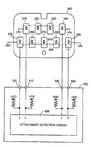
performed by the use of one or two terminals among many provided in the
cartridge. However, even if proper attachment of the cartridge is detected,
other terminals not used for the attachment detection may have poor contacts
with those of the printing apparatus. Especially when the terminals for a
memory device are in poor contact, a problem arises that errors tend to occur
when data are written or read from or to the memory device.
[0046] Such a problem of poor contact of terminals is critical especially when
it
comes to cartridges for large format inkjet printers that prints on large-size
paper (e.g. A2-A0 sizes) such as posters. In other words, cartridge dimensions
of large format inkjet printers are larger than those of cartridges for small
format inkjet printers, and the amount of ink contained in the cartridge is
larger in the former than the latter. Judging from these differences in
dimensions and weights, the inventors have found out that the ink cartridges
of
large format inkjet printers have more tendency to tilt than those of small
format inkjet printers. Also, the location of the engagement between the ink
cartridge and cartridge holder (also called "cartridge attachment unit") is
often
positioned on the side surface of the ink cartridge, whereas such engagement
of
small format inkjet printer is often located on the bottom surface of the ink
cartridge. In light of this location difference of the engagement, it has been
found that ink cartridges of large format inkjet printers are more likely to
tilt
than those of small format inkjet printers. Thus, in large format inkjet
printers, ink cartridges are more likely to tilt due to various configurations
as
compared to those of small format inkjet printers, and as a result, poor
contact
conditions are likely to occur at the circuit board terminals. Therefore, the
inventors have come to expect that proper contact conditions at the memory
device terminals should be detected more accurately especially in case of
large
format inkjet printers.
[0047] Fig. 3A shows a surface configuration of the board 200. The surface of
the board 200 is a plane exposed to outside when the board 200 is attached to
the cartridge 100. Fig. 3B shows a side view of the board 200. A boss groove
201 is formed on the top part of the board 200, and a boss hole 202 is formed
on
CA 02768790 2012-02-07
24
the bottom part of the board 200.
[0048] The arrow SD in Fig. 3A shows the attachment direction of the
cartridge 100 to the cartridge attachment unit 1100. This attachment
direction SD coincides with the attachment direction (X direction) of the
cartridge shown in Figs. 2A and 2B. The board 200 has a memory device 203
on its rear surface, and its front surface is provided with a group of
terminals
composed of nine terminals 210-290.
These terminals 210-290 have
approximately the same height from the surface of the board 200, and are
arranged thereon in a two-dimensional way. The memory device 203 stores
information on ink (e.g. remaining amount of ink) in the cartridge 100. The
terminals 210-290 are each formed in a rectangular shape and arranged so as
to form two rows approximately perpendicular to the attachment direction SD.
Among the two rows, the one on the front side of the attachment direction SD
(upper row in Fig. 3A) is called the upper row R1 (first row), and the one on
the
farther side of the attachment direction SD (lower row in Fig. 3A) is called
the
lower row R2 (second row). Also, it is possible to consider these rows R1 and
R2 as formed by contact portions cp of the plural terminals. A group of
terminals on the printing apparatus side (described later) get in contact with
the terminals 210-290 on the board 200 at these contact portions cp. Each
contact portion is in an approximate shape of a point having much smaller area
than that of each terminal. When the cartridge 100 is attached to the printing
apparatus, contact portions of a group of terminals on the printing apparatus
side slide upward on the board 200 from the bottom end in Fig. 3A, and stop at
the positions where the respective cartridge-side terminals are in contact
with
all the corresponding apparatus-side terminals when the attachment is
completed.
[0049] The terminals 210-240 forming the upper row R1 and the terminals
250-290 forming the lower row R2 have the following functions or uses
respectively:
<Upper row R1>
(1) Attachment detection terminal 210
CA 02768790 2012-02-07
(2) Reset terminal 220
(3) Clock terminal 230
(4) Attachment detection terminal 240
<Lower row R1>
5 (5) Attachment detection terminal 250
(6) Power terminal 260
(7) Ground terminal 270
(8) Data terminal 280
(9) Attachment detection terminal 290
10 [0050] The four attachment detection terminals 210, 240, 250 and 290 are
used
for detecting the conditions of electrical contact with the corresponding
apparatus-side terminals, and these terminals may alternately be called
"contact detection terminals." The attachment detection process may also be
called "contact detection process." Five other terminals 220, 230, 260, 270
and
15 280 are terminals for the memory device 203, which may also be called
"memory terminals."
[0051] Each of the plural terminals 210-290 contains in its center a contact
portion cp that gets in contact with the corresponding terminal among plural
apparatus-side terminals. All contact portions cp of terminals 210-240 that
20 form the upper row R1 and all contact portions cp of terminals 250-290
that
form the lower row R2 are arranged in an alternate manner, making up
so-called a staggered or zigzag pattern. Likewise, the terminals 210-240
forming the upper row R1 and the terminals 250-290 forming the lower row R2
are arranged in an alternate manner to make up a staggered or zigzag pattern
25 so as not to have their respective terminal centers aligned in the
attachment
direction SD.
[0052] Contact portions of the two attachment detection terminals 210 and 240
of the upper row R1 are placed at both ends of the upper row R1 respectively,
that is, on the outer edges of the upper row R1. Also, contact portions of the
two attachment detection terminals 250 and 290 of the lower row R2 are placed
at both ends of the lower row R2 respectively, that is, on the outer edges of
the
CA 02768790 2012-02-07
26
lower row R2. Contact portions of the memory terminals 220, 230, 260, 270
and 280 are placed at an approximate center of the area within which the group
of plural terminals 210-290 are arranged. Also, contact portions of the four
attachment detection terminals 210, 240, 250 and 290 are placed at four
corners of the area defined by the cluster of memory terminals 220, 230, 260,
270 and 280.
[0053] Fig. 3C shows contact portions 210cp-290cp of the nine terminals
210-290 of Fig. 3A. These nine contact portions 210cp-290cp are arranged
with almost constant intervals in an approximately even distribution. The
plural contact portions 220cp, 230cp, 260cp, 270cp and 280cp for the memory
device are placed in the central portion (first area) 810 of an area within
which
the group of terminal points 210cp-290cp are arranged. Contact portions
210cp, 240cp, 250cp and 290cp of the four attachment detection terminals are
placed outside the first area 810. Also, contact portions 210cp, 240cp, 250cp
and 290cp of the four attachment detection terminals are placed at four
corners
of a second area 820 having a quadrangular shape that encompasses the first
area 810. The shape of the first area 810 is preferably a quadrangle with a
minimum area encompassing contact portions 210cp, 240cp, 250cp and 290cp of
the four attachment detection terminals. Or, the shape of the first area 810
may be a quadrangle that circumscribes contact portions 210cp, 240cp, 250cp
and 290 cp of the four attachment detection terminals. The shape of the
second area 820 is preferably be a quadrangle with a minimum area
encompassing all of the terminal points 210cp-290cp. Also, when viewed in
the vertical direction ( - Z direction) in Fig. 2B, the center of the first
area 810
containing the plural contact portions 220cp, 230cp, 260cp, 270cp and 280cp
for
the memory device is preferably arranged to align with the center line of the
ink supply outlet 110 (Fig. 2B) of the cartridge 100.
[0054] In this embodiment, the second area 820 is of a trapezoidal shape. The
shape of the second area may be preferably an isosceles trapezoid having a
smaller top base (first base) than a bottom base (second base). In the
CA 02768790 2012-02-07
27
condition where the attachment of the cartridge 100 to the printing apparatus
is completed, contact portions 210cp, 240cp, 250cp and 290cp of the four
attachment detection terminals 210, 240, 250 and 290 are preferably placed
close at both ends of the top base and bottom base of the second area 820 in a
trapezoidal shape (i.e. at both ends of upper row R1 and lower row R2 in Fig.
3A). The reason for this is as follows. Under the condition where the
cartridge 100 is attached to the printing apparatus, an ink supply outlet 110
(see Fig. 2B) of the cartridge 100 is connected to an ink supply pipe
(described
later) of the printing apparatus. Therefore, if the cartridge 100 gets tilted
centered around the ink supply outlet 110 from the normal attachment position
in the Y direction, it is highly possible that the contact portion of the
terminal
farthest from the ink supply outlet 110 is displaced from the center of the
terminal by the longest distance. In this embodiment, among the terminals
210-240 in the upper row R1, the terminals located farthest from the ink
supply
outlet 110 are the attachment detection terminals 210 and 240 at both ends of
the upper row R1. Among the terminals 250-290 in the lower row R2, the
terminals located farthest from the ink supply outlet 110 are the attachment
detection terminals 250 and 290 at both ends of the lower row R2. If two rows
of terminals are arranged not in a staggered pattern but in a rectangular
pattern (or a matrix-like pattern), the second area 820 including contact
portions cp on the board 200 becomes a rectangle, too. In that case, the
attachment detection terminals 210 and 240 aligned in the upper row R1 are
positioned farther from the ink supply outlet 110 than the attachment
detection
terminals 250 and 290, so that the former terminals get displaced farther from
the corresponding apparatus-side terminals. At this time, even if other
terminals 220, 230, 250-290 are under proper contact conditions, contacts of
the
attachment detection terminals 210 and 240 in the upper row R1 may not be
sufficient so that they can be misjudged as poor contact. Therefore, in order
to
reduce such a risk of misjudgment, contact portions 210cp, 240cp, 250cp and
290cp of the four attachment detection terminals 210, 240, 250 and 290 are
preferably placed at both ends of the upper base and bottom base of the second
CA 02768790 2012-02-07
28
area 820 in a trapezoidal shape. The advantage of arranging the shape of the
second area 820 including all contact portions on the board 200 is more or
less
the same in case of other embodiments described later.
[0055] Figs. 4A-4C are diagrams showing a configuration of the cartridge
attachment unit 1100. Fig. 4A is a perspective view seen diagonally from
behind the cartridge attachment unit 1100, while Fig. 4B is a front view (on
the
side where the cartridge is inserted) into the interior of the cartridge
attachment unit 1100. Fig. 4C is a sectional view of the interior of the
cartridge attachment unit 1100. In Figs. 4A-4C, some partitions and other
elements are omitted for the convenience of illustration. The X, Y and Z axes
in Figs. 4A-4C correspond to those in Figs. 2A and 2B. The cartridge
attachment unit 1100 is provided with four holding slots SL1-SL4 for holding
cartridges. As shown in Fig. 4B, inside the cartridge attachment unit 1100,
each slot is equipped with an ink supply tube 1180, a pair of positioning pins
1110 and 1120, a comb joint 1140, and a contact mechanism 1400. As shown in
Fig. 4C, the ink supply tube 1180 , the pair of positioning pins 1110 and
1120,
and the comb joint 1140 are fixed to the back wall member 1160 of the
cartridge
attachment unit. The ink supply tube 1180, the positioning pins 1110 and
1120, and the comb joint 1140 are inserted through holes 1181, 1111, 1121 and
1141 provided on a slider member 1150 and are placed to protrude in the
direction opposite to the insertion direction of the cartridge. Fig 4A is a
perspective view seen from behind the slider member 1150 with the back wall
member 1160 removed. Positioning pins are omitted in Fig. 4A. As shown in
Fig. 4A, a pair of bias springs 1112 and 1122 that correspond to the pair of
positioning pins 1110 and 1120 are provided on the rear side of the slider
member 1150. As shown in Fig. 4C, the pair of bias springs 1112 and 1122 are
fixed in place to the slider member 1150 and back wall member 1160.
[0056] The ink supply tube 1180 is inserted into the ink supply outlet 110
(Fig.
2A) of the cartridge 100 to be used for supplying ink to the print head inside
the
printing apparatus 1000. The positioning pins 1110 and 1120 are inserted into
the positioning holes 131 and 132 provided in the cartridge 100 to be used for
CA 02768790 2012-02-07
29
determining the holding position of the cartridge 100 when the cartridge 100
is
inserted into the cartridge attachment unit 1100. The comb joint 1140 has a
shape corresponding to that of the comb joint 134 of the cartridge 100 and is
different in shape from each other in each of the holding slots SL1-SL4. This
allows each of the holding slots SL1-SL4 to accept only the cartridge
containing
a prescribed type of ink and exclude cartridges of other colors.
[0057] The slider member 1150 placed on the back wall in each holding slot is
configured to be slidable in the attachment and detachment directions of the
cartridge (X direction and ¨X direction, respectively). The pair of bias
springs
1112 and 1122 (Fig. 4A) exert a biasing force on the slider member 1150 in the
detachment direction. The cartridge 100, together with the slider member
1150, pushes the pair of bias springs 1112 and 1122 in the attachment
direction
when inserted into the holding slot to be pushed in against the force of the
bias
springs 1112 and 1122. Therefore, the cartridge 100, when placed in the
cartridge attachment unit 1100, gets biased in the detachment direction by the
pair of bias springs 1112 and 1122. Under these conditions where the
cartridge is in place, a stopper member 1130 (Fig. 4B) placed at the bottom of
each of the holding slots SL1-SL4 is engaged with the stopper groove 140 (Fig.
2A) placed at the bottom surface Sb of the cartridge 100. This engagement
between the stopper member 1130 and stopper groove 140 prevents the
cartridge 100 from being detached from the cartridge attachment unit 1100 by
the force of bias springs 1112 and 1122.
[0058] When the user pushes in the cartridge 100 in the attachment direction
to dismount the cartridge 100, the stopper member 1130 is disengaged from the
stopper groove 140 in response to the push. As a result, the cartridge 100 is
pushed over in the detachment direction (¨X direction) by the force of the
pair
of bias springs 1112 and 1122. Thus, the user may easily remove the cartridge
100 from the cartridge attachment unit 1100.
[0059] The contact mechanism 1400 (Fig. 4B) includes plural apparatus-side
terminals that get in contact with the terminals 210-290 (Fig. 3A) of the
circuit
board 200 to conduct electricity when the cartridge 100 is inserted into the
CA 02768790 2012-02-07
cartridge attachment unit 1100. The control circuit of the printing apparatus
1000 sends and receives signals to and from the circuit board 200 via this
contact mechanism 1400.
[0060] Fig. 5A shows proper attachment of the cartridge 100 in the cartridge
5 attachment unit 1100. In this situation, the cartridge 100 is not tilted
and its
upper and bottom surfaces are in parallel with the upper and lower members of
the cartridge attachment unit 1100. The ink supply tube 1180 of the cartridge
attachment unit 1100 is connected to the ink supply outlet 110, while the
positioning pins 1110 and 1120 of the cartridge attachment unit 1100 are
10 inserted into the positioning holes 131 and 132. In addition, the stopper
member 1130 provided at the bottom of the cartridge attachment unit 1100 is
engaged with the stopper groove 140 provided at the bottom of the cartridge
100. Then, the cartridge's front surface Sf receives a biasing force in the
detachment direction by the pair of bias springs 1112 and 1122 in the
cartridge
15 attachment unit 1100. Under the condition where the cartridge 100 is
properly attached, the contact mechanism 1400 of the cartridge attachment
unit 1100 and the terminals 210-290 (Fig. 3A) on the circuit board 200 of the
cartridge 100 are in good contact with each other.
[0061] Meanwhile, the cartridge attachment unit 1100 has a small allowance
20 within it in order to accommodate easy attachment of the cartridge 100.
For
this reason, the cartridge 100 does not necessarily get attached in a proper
upright position as shown in Fig. 5A but may possibly tilt around an axis
parallel to the cartridge's width direction (Y direction). More specifically,
as
shown in Fig. 5B, it sometimes tilts with its rear end sagging, or conversely
as
25 shown in Fig. 5C, it may tilt with its rear end slightly lifted.
Especially as ink
is consumed and the liquid level LL drops down, the gravity center shifts in
response to the weight reduction of ink contained, and the balance between the
force by the bias springs 1112, 1122 and the weight of the cartridge including
ink gets shifted. According to this change in weight balance, the cartridge is
30 more likely to tilt. When the cartridge tilts, some of the plural terminals
placed on the cartridge's circuit board 200 may experience poor contact.
CA 02768790 2012-02-07
31
Especially under the conditions of Fig. 5B and 5C, one or more terminals in
either the group of terminals 210-240 in the upper row R1 or the group of
terminals 250-290 in the lower row R2 may possibly experience poor contact.
[0062] Additionally, when the cartridge tilts, another form of tilt may also
happen in the direction perpendicular to the one shown in Fig. 5B or 5C (a
tilt
around an axis parallel to the attachment direction X). In this case, the
board
200 also tilts to the right or left around an axis perpendicular to its
attachment
direction SD, which may cause poor contact at one or more terminals of either
the group of terminals 210, 220, 250 and 260 on the left side of the board 200
or
the group of terminals 230, 240, 280 and 290 on the right side thereof.
[0063] Once such poor contact occurs, it leads to a failure wherein sending
and
receiving of signals between the cartridge's memory device 203 and the
printing
apparatus 1000 may not be performed properly any more. Also, if the area
around the board 200 is contaminated with foreign matters such as dust and
droplets of ink, unintended shorting or leak may happen between the terminals.
The processes of attachment detection according to various embodiments
explained below may be performed to detect poor contact arising from the
above-mentioned tilting of the cartridge or unintended shorting or leak caused
by foreign matters.
[0064] Meanwhile, as compared to cartridges for small format inkjet printers
for individual users, cartridges for large format inkjet printers have the
following characteristics:
(1) Cartridge dimensions are larger (the length L1 is 100mm or more).
(2) More amount of ink contained (no less than 17m1, typically 100m1 or
more).
(3) Mechanically engaged with the cartridge attachment unit on the
front surface (frontend plane in the attachment direction).
(4) The space inside the ink container is not partitioned, forming a
single ink container (or ink bag).
Depending on the type of large format inkjet printers, some cartridges
lack some of the characteristics (1)-(4), but most cartridges typically have
at
CA 02768790 2012-02-07
32
lease one of them.
[0065] Cartridges for large format inkjet printers are more likely to tilt
than
those for small format inkjet printers due to the above characteristics
pertaining to dimensions, weight, the location of connections with the
cartridge
attachment unit, or the configuration of the ink container, and as a result,
poor
contact at the terminals of the board 200 is likely to happen. Therefore, it
is of
great significance to perform processes as described below to detect poor
contact, unintended shorting, and leak at the terminals for the large format
printers and their cartridges.
[0066] Fig. 6 is a block diagram showing an electrical configuration of the
ink
cartridge's board 200 and the printing apparatus 1000 according to the first
embodiment. The printing apparatus 1000 includes a display panel 430, a
power circuit 440, a main control circuit 400, and a sub-control circuit 500.
The display panel 430 is used for sending various messages to the users on the
operating status of the printing apparatus 1000 and attachment conditions of
the cartridge. The display panel 430 is installed, for example, at the
operation
unit 1300 in Fig. 1. The power circuit 440 includes a first power source 441
that generates a first power supply voltage VDD and a second power source 442
that generates a second power supply voltage VHV. The first power supply
voltage VDD is a common power voltage used for logic circuits (e.g. rated
3.3V).
The second power supply voltage VHV is a higher voltage (e.g. rated 4.2V) to
be
used for driving the print head to eject ink. These voltages VDD and VHV are
supplied to the sub-control circuit 400 as well as to other circuits as
necessary.
The main control circuit 400 includes a CPU 410 and a memory 420. The
sub-control circuit 500 includes a memory control circuit 501 and an
attachment detection circuit 600. It is possible to collectively call the main
control circuit 400 and the sub-control circuit 500 a "control circuit."
[0067] Among the nine terminals provided on the cartridge's board 200 (Fig.
3)A, the reset terminal 220, clock terminal 230, power terminal 260, ground
terminal 270 and data terminal 280 are electrically connected to the memory
device 203. The memory device 203 is a non-volatile memory with no address
CA 02768790 2012-02-07
33
terminal that receives data from the data terminal or sends data from the data
terminal in synchronous with the clock signal SCK, wherein accessible memory
cells are determined based on the number of pulses of the clock signal SCK
inputted from the clock terminal and the command data inputted from the data
terminal. The clock terminal 230 is used for supplying the clock signal SCK
from the sub-control circuit 500 to the memory device 203. The power voltage
(e.g. rated 3.3V) and ground voltage (OV) for driving the memory device are
supplied from the printing apparatus 1000 to the power terminal 260 and
ground terminal 270, respectively. The power voltage for driving the memory
device 203 may be a voltage directly given by the first power supply voltage
VDD or the one generated therefrom, which is lower than the first power
supply voltage VDD. The data terminal 280 is used for transmitting data
signals SDA between the sub-control circuit 500 and memory device 203. The
reset terminal 220 is used for supplying reset signals RST from the sub-
control
circuit 500 to the memory device 203. The four attachment detection
terminals 210, 240, 250, 290 are connected with each other via wiring inside
the board 200 of the cartridge 100 (Fig. 3A), which are all grounded. For
example, the grounding of the attachment detection terminals 210, 240, 250,
290 is done by connecting them to the ground terminal 270. However, the
grounding via a route other than the ground terminal is permissible. As seen
from the above explanation, the attachment detection terminals 210, 240, 250
and 290 may be connected to part of the memory terminals (or the memory
device 203), but preferably should not be connected to any memory terminal or
memory device other than the ground terminal. Especially, it is preferable, in
terms of ensuring the performance of attachment detection, that the
attachment detection terminals are connected to none of the memory terminals
or memory device, because no signal or voltage other than the attachment
detection signal is applied to the attachment detection terminals. The four
attachment detection terminals 210, 240, 250 and 290 are connected via wiring
in the example of Fig. 6, but part of the wiring may be replaced with some
resistances. Here, a connection between two terminals by a wiring may be
CA 02768790 2012-02-07
34
called "short-circuit connection" or "conductive connection." The short-
circuit
connection is a different state from that of unintended shorting.
[0068] In Fig. 6, the wiring routes between the sub-control circuit 500 and
the
board 200 that connect the apparatus-side terminals 510-590 with the
terminals 210-290 of the board 200 are coded SCK, VDD, SDA, RST, OV1, 0V2,
DT1 and DT2. Among these wiring codes, the one for the wiring of the
memory device is coded the same as the signal name.
Here, the
apparatus-side terminals 510-590 are provided in the contact mechanism 1400
shown in Figs. 4B and 5A.
[0069] Fig. 7 shows connection between the board 200 and the attachment
detection circuit 600. The four attachment detection terminals 210, 240, 250
and 290 on the board 200 are connected to the attachment detection circuit 600
via the corresponding apparatus-side terminals 510, 540, 550 and 590. Also,
the four attachment detection terminals 210, 240, 250 and 290 on the board 200
are grounded. The wiring that connects the apparatus-side terminals 510, 540,
550 and 590 with the attachment detection circuit 600 are each connected to
the power supply voltage VDD (rated 3.3V) within the sub-control circuit 500
via a pull-up resistance.
[0070] In the example of Fig. 7, the three terminals 210, 240 and 250 among
the four attachment detection terminals 210, 240, 250 and 290 on the board-200
are in good contact with the corresponding apparatus-side terminals 510, 540
and 550. On the other hand, the fourth attachment detection terminal 290 is
not in contact with the corresponding apparatus-side terminal 590. The
wiring voltage of the three apparatus-side terminals 510, 540 and 550 that are
in good contact turns to L level (ground voltage level), whereas the wiring
voltage of the apparatus-side terminal 590 that is not in contact turns to H
level (power supply voltage VDD). Therefore, it is possible for the attachment
detection circuit 600 to detect contact conditions for each of the four
attachment
detection terminals 210, 240, 250 and 290 by checking each voltage level of
such wiring.
[0071] Contact portions cp of the four attachment detection terminals 210,
240,
CA 02768790 2012-02-07
250 and 290 on the board 200 are each placed at four corners along the
periphery of the cluster area 810 defined by contact portions cp of the
terminals
220, 230, 260, 270 and 280 for the memory device. When all the contacts of
the four attachment detection terminals 210, 240, 250 and 290 are in good
5 condition, the cartridge does not tilt much and the contact conditions of
the
terminals 220, 230, 260, 270 and 280 are in good condition, too. On the
contrary, one or more terminals among the four attachment detection terminals
210, 240, 250 and 290 are in poor contact, the cartridge has a significant
tilt
and one or more terminals among the terminals 220, 230, 260, 270 and 280 for
10 the memory device may possibly in poor contact. If one or more terminals
among the four attachment detection terminals 210, 240, 250 and 290 are in
poor contact, the attachment detection circuit 600 may preferably display
information (by words or images) on the display panel 430 notifying the user
of
the non-attached condition.
15 [0072] Meanwhile, the reason for providing contact portions cp of the
attachment detection terminals at all four corners along the periphery of the
cluster area 810 defined by contact portions of the memory device terminals is
that the board 200 of the cartridge 100 and the contact mechanism 1400 of the
cartridge attachment unit 1100 (Fig. 5A) may sometimes tilt relative to each
20 other due to a degree of freedom in the cartridge 100 to tilt to some
extent even
in the situation where the cartridge 100 is attached to the cartridge
attachment
unit 1100. For example, if the rear end of the cartridge 100 tilts as shown in
Fig. 5B to let the group of terminals 210-240 (or their contact portions) of
upper
row R1 shift away from the contact mechanism 1400 farther than the group of
25 terminals 250-290 (or their contact portions) of the lower row R2, the
group of
terminals 210-240 of the upper row R1 may result in poor contact. On the
contrary, if the rear end of the cartridge 100 tilts as shown in Fig. 5C to
let the
group of terminals 250-290 of the lower row R2 on the board 200 shift away'
from the contact mechanism 1400 farther than the group of terminals of the
30 upper row R1, the five terminals 250-290 of the lower row R2 on the
board 200
may result in poor contact. Also, unlike Figs. 5B and 5C, if the cartridge 100
CA 02768790 2012-02-07
36
tilts around an axis parallel to the X-direction to let the left edge of the
board
200 in Fig. 7 shift away from the contact mechanism 1400 farther than the
right edge, the terminals 210, 220, 250, 260 and 270 on the left sided of the
board 200 may result in poor contact,. On the contrary, the right edge of the
board 200 shifts farther from the contact mechanism 1400 than the left edge,
the terminals 230, 240, 270, 280 and 290 on the right side of the board 200
may
result in poor contact. Once such a contact failure occurs, some errors may be
caused in writing and reading data to and from the memory device 203.
Therefore, as mentioned above, if all the contact conditions are confirmed,
whether they are good or poor, at contact portions of the four attachment
detection terminals 210, 240, 250 and 290 placed at four corners of the
cluster
area 810 defined by the contact portions of the memory terminals 220, 230,
260,
270 and 280, it is possible to prevent any contact failure and access error of
the
memory device caused by such tilting as described above.
[0073] Since the first embodiment is provided with contact portions of the
attachment detection terminals placed at four corners along the periphery of
the cluster area defined by the contract points of the plural memory device
terminals on the board, it is possible to secure good contact conditions for
memory device terminals by confirming good contact between the attachment
detection terminals and the corresponding apparatus-side terminals.
Especially in case of cartridges for large format inkjet printers, the
cartridge is
likely to tilt within the cartridge attachment unit, as explained in Figs. 5A-
5C.
Therefore, the necessity and meaning of placing contact portions of the four
attachment detection terminals at four corners of the area along the periphery
of the area where contact portions of plural memory device terminals are
placed
(outside the area where contact portions of plural memory device terminals are
placed and encompassing such area), as well as confirming all the contact
conditions of the four attachment detection terminals, whether they are good
or
poor, are considered significant especially regarding cartridges for large
format
inkjet printers. Here, the word "plural memory device terminals" means two
power terminals (ground terminal, power terminal) and three signal terminals
CA 02768790 2012-02-07
37
(reset terminal, clock terminal, data terminal) which are required for the
control circuit of the printing apparatus to write or read data to and from
the
memory device provided in the cartridge.
[0074]
B. Second embodiment:
Fig. 8 is a diagram showing the circuit board configuration according to
the second embodiment. The arrangement of the terminals 210-290 is the
same as that shown in Fig. 3A. However, functions or uses of various
terminals are slightly different from those of the first embodiment as
follows.
[0075]
<Upper row R1>
(1) Overvoltage detection terminal 210 (also used for leak detection and
attachment detection)
(2) Reset terminal 220
(3) Clock terminal 230
(4) Overvoltage detection terminal 240 (also used for leak detection and
attachment detection)
<Lower row R1>
(5) Sensor terminal 250 (also used for attachment detection)
(6) Power terminal 260
(7) Ground terminal 270
(8) Data terminal 280
(9) Sensor terminal 290 (also used for attachment detection)
[0076] The terminals 210 and 240 located at both ends of the upper row R1 and
their contact portions are used for detecting overvoltage (explained later),
leak
between terminals (explained later), and attachment (contact) conditions.
Also, the terminals 250 and 290 of the lower row R2 and their contact portions
are used for detecting the remaining amount of ink using a sensor provided in
the cartridge 100 as well as for attachment (contact) detection. As in the
first
embodiment, the four contact portions of the terminals 210, 240, 250 and 290
CA 02768790 2012-02-07
38
located at four corners of the quadrangular area including contact portions of
the group of terminals 210-290 are used for attachment detection (contact
detection). In the second embodiment, however, the same voltage as the first
power supply voltage VDD for driving the memory device, or a voltage
generated from the first power supply voltage VDD is applied to contact
portions of the two terminals 210 and 240 placed at both ends of the upper row
R1, and the same voltage as the second power supply voltage VHV used for
driving the print head, or a voltage generated from the second power supply
voltage VHV is applied to contact portions of the two terminals 250 and 290
placed at both ends of the lower row R2. As the "voltage generated from the
first power supply voltage VDD," it is preferable to use a voltage that is
lower
than the first power supply voltage VDD (ordinarily 3.3V) but higher than the
ground voltage, and more preferably, a voltage that is lower than an
"overvoltage threshold value" which is applied to the terminal 210 or 240 when
an overvoltage is detected by an overvoltage detection unit described later.
As
the "voltage generated from the second power supply voltage VHV," it is
preferable to use a voltage that is higher than the first power supply voltage
VDD but lower than the second power supply voltage VHV.
[0077] On the board 200a in Fig. 8, as is the case for the board 200 in Fig.
3A,
contact portions of the four attachment detection terminals 210, 240, 250 and
290 are placed close at both ends of the upper base and bottom base of the
trapezoidal area. Therefore, compared to the situation where those contact
portions of the attachment detection terminals are placed at four corners of a
rectangle, there is an advantage of a lower risk of misjudgments concerning
the
attachment conditions.
[0078] By the way, as one of the aspects of attachment detection or contact
detection of a printing material cartridge, a shorting detection is sometimes
performed to check if there is any unintended shorting between the cartridge
terminals. If a shorting detection is to be performed, a shorting detection
terminal is placed at a location adjacent to a high-voltage terminal where a
voltage higher than the regular power supply voltage (3.3V) is applied in
order
CA 02768790 2012-02-07
39
to detect an overvoltage at the shorting detection terminal. And, if any such
overvoltage is detected at the shorting detection terminal, the high voltage
applied to the high-voltage terminal is stopped. However, even if the high
voltage is stopped when overvoltage is detected at the shorting detection
terminal, a problem remains that a possibility cannot be ruled out that some
failures might occur in the cartridge or printing apparatus caused by the
overvoltage that had been generated before the stoppage. The second and
third embodiments described below include some measures to solve such a
conventional problem.
[0079] Fig. 9 is a block diagram showing an electrical configuration of the
ink
cartridge's circuit board 200a and the printing apparatus 100 according to the
second embodiment. The board 200a is provided with a sensor 208 used for
detecting the remaining amount of ink in addition to the memory device 203
and nine terminals 210-290. As the sensor 208, a known sensor for the
remaining amount of ink using piezo-electric elements may be used. A
piezo-electric element electrically functions as a capacitative element.
[0080] The main control circuit 400 includes a CPU 410 and a memory 420 as
in the first embodiment. The sub-control circuit 500a includes a memory
control circuit 501 and a sensor-related-processing circuit 503. The
sensor-related-processing circuit 503 is used for detecting attachment
conditions of the cartridges in the cartridge attachment unit 1100 and
detecting
the remaining amount of ink using the sensor 208.
Since the
sensor-related-processing circuit 503 is used for detecting attachment
conditions of the cartridge, it may also be called a "attachment detection
circuit." The sensor-related-processing circuit is a high voltage circuit that
applies or supplies a higher voltage to the cartridge sensor 208 than the
power
supply voltage VDD that is applied or supplied to the memory device 203. The
high voltage applied to the sensor 208 may be the power supply voltage VHV
(rated 42V) itself used for driving the print head or a slightly lower voltage
(e.g.
36V) generated from the power supply voltage VHV used for driving the print
head.
CA 02768790 2012-02-07
[0081] Fig. 10 is a diagram showing the internal configuration of a
sensor-related-processing circuit 503 according to the second embodiment.
Here, four cartridges are shown as attached in the cartridge attachment unit,
and reference codes IC1-1C4 are used to identify each cartridge. The
5 sensor-related-processing circuit 503 includes a non-attached condition
detection unit 670, an overvoltage detection unit 620, a detection pulse
generation unit 650 and a sensor processing unit 660. The sensor processing
unit 660 includes a contact detection unit 662 and a liquid volume detection
unit 664. The contact detection unit 662 detects the contact conditions of the
10 sensor terminals 250 and 290 using the cartridge sensor 208. The liquid
volume detection unit 664 detects the remaining amount of ink using the
cartridge sensor 208. The detection pulse generation unit 650 and the
non-attached condition detection unit 670 perform detection of whether all the
cartridges are attached (detection process of non-attached conditions), and
15 detection of any leak between terminals 210 and 250 as well as between
terminals 240 and 290. The overvoltage detection unit 620 performs detection
of whether any overvoltage is applied to the overvoltage detection terminal
210
or 240. The overvoltage detection may be also referred to as "short-circuit
detection", and the overvoltage detection unit 620 may be also referred to as
20 "short-circuit detection circuit 620."
[0082] In each cartridge, the first and second overvoltage detection terminals
210 and 240 are connected with each other via wiring. In the example of Fig.
10, the overvoltage detection terminals 210 and 240 are in short-circuit
connection via wiring, but part of the wiring may be replaced with some
25 resistance. The first overvoltage detection terminal 210 of the first
cartridge
IC1 is connected to the wiring 651 within the sensor-related-processing
circuit
503 via the corresponding apparatus-side terminal 510, and the wiring 651 is
in
turn connected to the non-attached condition detection unit 670. The second
overvoltage detection terminal 240 of the nth (n =1-3) cartridge and the first
30 overvoltage detection terminal 210 of the (n+1)th cartridge are
connected with
each other via the corresponding apparatus-side terminals 540 and 510. Also,
CA 02768790 2012-02-07
41
the second overvoltage detection terminal 240 of the fourth cartridge IC4 is
connected to the detection pulse generation unit 650 via the corresponding
apparatus-side terminal 540. If all of the cartridges IC1-1C4 are attached
properly within the cartridge attachment unit, the detection pulse generation
unit 650 and the non-attached condition detection unit 670 get connected with
each other via the overvoltage detection terminals 240 and 210 on the
cartridges in sequence. On the other hand, if any cartridge is not attached or
improperly attached, non-contact or poor contact occurs at either of the
apparatus-side terminals 510 and 540 or any of the terminals 210 and 240 of
the cartridges IC1-1C4, resulting in a condition of non-contact between the
detection pulse generation unit 650 and the non-attached condition detection
unit 670. Therefore, the non-attached condition detection unit 670 is able to
detect whether there is any non-contact or poor contact condition at either of
the overvoltage detection terminals in the cartridges IC1-1C4 depending on
whether it receives a response signal DPres that correspond to an inspection
signal DPins sent from the detection pulse generation unit 650. Thus, in the
second embodiment, since the overvoltage detection terminals 240 and 210 of
the cartridges are series-connected in series when all the cartridges IC1-1C4
are attached in the cartridge attachment unit, it is possible to detect
whether
there is any non-contact or poor contact condition at any of the overvoltage
detection terminals 210 and 240 in the cartridges IC1-1C4 by inspecting the
contact conditions. A typical situation where such non-contact or poor contact
condition occurs is when one or more cartridges are not attached. Therefore,
the non-attached condition detection unit 670 is able to detect immediately
whether one or more cartridges are not attached depending on whether it
receives a response signal DPres corresponding to an inspection signal DPins.
The inspection signal DPins may be generated based on the voltage supplied
from the first power supply VDD.
[0083] The first overvoltage detection terminals 210 of the four cartridges
IC1-1C4 are also connected to anode terminals of diodes 641-644 via the
corresponding apparatus-side terminals 510. Also, the second overvoltage
CA 02768790 2012-02-07
42
detection terminals 240 of the four cartridges IC1-1C4 are connected to anode
terminals of diodes 642-645 via the corresponding apparatus-side terminals
540. Meanwhile, the anode terminal of the second diode 642 is connected in
common to the second overvoltage detection terminal 240 of the first cartridge
IC1 and the first overvoltage detection terminal 210 of the second cartridge
IC2.
Equally, the diodes 643 and 644 are each connected in common to the first
overvoltage detection terminal 210 of a cartridge and to the second
overvoltage
detection terminal 240 of an adjacent cartridge. Cathode terminals of these
diodes 641-645 are connected in parallel to the overvoltage detection unit
620.
These diodes 641-645 are used to monitor any abnormally high voltage to the
overvoltage detection terminals 210 and 240. Such an abnormally high
voltage (called "overvoltage") occurs when unintended shorting occurs between
either of the overvoltage detection terminals 210 and 240 in each cartridge
and
either of the sensor terminals 250 and 290. For example, if foreign matters
such as ink droplets or dust are attached to the surface of the board 200
(Fig3A),
unintended shorting may possibly occur between the first overvoltage detection
terminal 210 and first sensor terminal 250, or between the second overvoltage
detection terminal 240 and second sensor terminal 290. Once any such
unintended shorting occurs, a current flows in the overvoltage detection unit
620 via one of the diodes 641-645 so that the overvoltage detection unit 620
can
detect that a voltage higher than a predetermined value (overvoltage) is
applied to an overvoltage terminal, and that the overvoltage detection unit
620
can detect any generation of overvoltage or unintended shorting. Also, foreign
matters that cause unintended shorting generally tend to come from the top
down of the board 200, and from the outside inward. Therefore, if the contact
portions of the overvoltage detection terminals 210 and 240 are arranged at
both ends of the contact portions aligned in the upper row R1 of the board 200
(Fig. 3A), the overvoltage detection terminals 210 and 240 are placed near the
sensor terminals 250 and 290, which allows to reduce the risk that the high
voltage applied to the sensor terminals 250 and 290 are also applied to the
memory terminals 200, 230, 260, 270 or 280.
CA 02768790 2012-02-07
43
[0084] Fig. 11 is a block diagram showing the condition of contact between the
cartridge sensor 208 and the contact detection unit 662 as well as the liquid
volume detection unit 664. The sensor 208 is connected selectively either to
the contact detection unit 662 or liquid volume detection unit 664 via a
selector
switch 666. In the situation where the sensor 208 is connected to the contact
detection unit 662, the contact detection unit 662 detects a good or poor
contact
between the sensor terminals 250, 290 and the corresponding apparatus-side
terminals 550, 590. On the other hand, in the situation where the sensor 208
is connected to the liquid volume detection unit 664, the liquid volume
detection unit 664 detects the remaining amount of ink within the cartridge to
find out if it is no less than a prescribed amount. The contact detection unit
662 operates under a comparatively low power supply voltage VDD (e.g. 3.3V).
On the contrary, the liquid volume detection unit 664 operates under a
comparatively high power voltage HV (e.g. 36V).
[0085] The contact detection unit 662 and liquid volume detection unit 664
may be provide individually per each cartridge, or a set of one contact
detection
unit 662 and one liquid volume detection unit 664 may be provided commonly
in each set of plural cartridges. In the latter case, a selection switch is
additionally provided to switch the connection between the sensor terminals
250 and 290 in each cartridge and the contact detection unit 662 as well as
the
liquid volume detection unit 664.
[0086] Fig. 12 is a set of timing charts showing various signals used for the
attachment detection process (also called "contact detection process") of the
cartridge according to the second embodiment. In the attachment detection
process of the cartridge, the first attachment detection signals DPins and
DPres as well as the second attachment detection signals SPins and SPres are
used. Here, the signals DPins and SPins with a suffix "ins" are signals
outputted from the sensor-related-processing circuit 503 to the cartridge's
board 200 and are called "attachment inspection signals." Also, the signals
DPres and SPres with a suffix "res" are signals inputted to the
sensor-related-processing circuit 503 from the cartridge's board 200 and are
CA 02768790 2012-02-07
44
called "attachment response signals."
[0087] As described below, the following three kinds of attachment detection
processes are performed in the second embodiment:
(1) First attachment detection process: Detection of non-attached
conditions of one or more cartridges using the first attachment detection
signals DPins and DPres (detection of contact conditions of the overvoltage
detection terminals 210 and 240 of all cartridges).
(2) Second attachment detection process: Detection of contact conditions
of the sensor terminals 250 and 290 in each cartridge using the second
attachment detection signals SPins and SPres.
(3) Leak detection process: Detection of a leak between the terminals
210 and 250 as well as between the terminals 240 and 290 using the first
attachment detection signals DPins and DPres.
[0088] Since contact conditions of the terminals are detected in the first and
second attachment detection processes, it is possible to call these processes
"contact detection processes." Also, the first and second attachment detection
signals may be called "the first contact detection signals DPins, DPres" and
"the second contact detection signals SPins, SPres."
[0089] The second attachment detection signals SPins and SPres are used by
the contact detection unit 662 to detect contact conditions of the sensor
terminals 250 and 290 in each cartridge. As shown in Fig. 10, the second
attachment detection signal SPins is supplied from the contact detection unit
662 to one sensor terminal 290, whereas the second attachment response signal
SPres returns to the contact detection unit 662 from the other sensor terminal
250. The second contact detection signal SPins turns to a high level H2 during
the first period P21 in Fig. 12 and later turns to a low level during the
second
period P22. Here, the high level voltage H2 of the second attachment
inspection signal SPins is set at 3.0V for example. When the terminals 250
and 290 are both in normal contact, the second attachment response signal
SPres shows the same pattern of level changes as the second attachment
inspection signal SPins.
CA 02768790 2012-02-07
[0090] As shown in Fig. 10, the first attachment inspection signal DPins is
supplied from the detection pulse generation unit 650 to the overvoltage
detection terminal 240 of the fourth cartridge IC4, whereas the first
attachment response signal DPres is inputted to the non-attached condition
5 detection unit 670 from the overvoltage detection terminal 210 of the first
cartridge IC1. As shown in Fig. 12, the first attachment inspection signal
DPins is divided into 7 periods P11-P17. That is, the first attachment
inspection signal DPins goes into a high impedance condition during the period
P11, and turns to a high level H1 during the periods P12, P14 and P16, and
10 turns to a low level in other periods P13, P15 and P17. The high level
voltage
H1 of the first attachment inspection signal DPins is set at 2.7V, which is
different from the high level H2 (3.0V) of the second attachment detection
signal SPins. Meanwhile, The first and second periods P11 and P12 of the
first attachment inspection signal DPins overlap part of the first period P21
of
15 the second attachment inspection signal SPins. Also, the fourth to seventh
periods P14-P17 of the first attachment inspection signal DPins overlap part
of
the second period P22 of the second attachment inspection signal SPins.
When the terminals 210 and 240 of all cartridges are in normal contact, the
first attachment response signal DPres turns to a low level during the first
20 period P11 showing the same pattern of levels as the first attachment
inspection signal DPins during the second period P12 and thereafter. The
reason why the first attachment response signal DPres turns to a low level
during the first period P11 is that the first attachment response signal DPres
(i.e. the wiring 651 that inputs to the non-attached condition detection unit
25 670) is at a low level immediately prior to the first period P11.
[0091] The voltage of the high level H1 of the first attachment inspection
signal DPins is preferably lower than the overvoltage (threshold value of
overvoltage) which is applied to the overvoltage detection terminals 210 and
240, and which is detected by the overvoltage detection unit 620. This is for
30 preventing any risk of erroneously judging the situation as overvoltage
during
the process of attachment detection using the first attachment inspection
signal
CA 02768790 2012-02-07
46
DPins. As the overvoltage value to be detected, 3.0V is used for example. In
the circuit diagram of Fig. 10, the overvoltage applied to the terminal 210 of
the
first cartridge IC1, for example, is inputted to the overvoltage detection
unit
620 via the diode 641. Therefore, the threshold value used by the overvoltage
detection unit 620 is the overvoltage value to be detected (e.g. 3.0V) less a
voltage drop of the diode 641 (e.g. 0.7V), resulting in 2.3V, for example. In
this
specification, the word "threshold value of overvoltage" may be used to denote
the voltage applied to the terminal 210 or 240 when an overvoltage at either
of
them is detected by the overvoltage detection unit 620.
[0092] Fig 13A shows signal waveforms when at least one of the terminals 250
and 290 is in poor contact. In this case, the second attachment response
signal
SPres turns to a low level throughout the periods P21 and P22. The contact
detection unit 662 is able to detect the contact conditions of the terminals
250
and 290, whether they are good or poor, by examining the level of the
attachment response signal SPres at a prescribed timing t21 during the period
P21. If any cartridge with poor contact at the terminal 250 or 290 is
detected,
the main control circuit 400 may preferably display information (by words or
images) on the display panel 430 to notify the user of a poor attachment
condition of the cartridge.
[0093] Fig. 13B shows waveforms when at least one of the terminals 210 and
249 in all cartridges is in poor contact. In this case, the first attachment
response signal DPres turns to a low level throughout the periods P11-P17.
Therefore, the non-attached condition detection unit 670 is able to detect
conditions where one or more cartridges are not attached normally by
examining the level of the first attachment response signal DPres at
prescribed
timings t12, t14 and t15 during the periods P12, P14 and P16 when the first
attachment inspection signal DPins turns to a high level. By the way, it is
enough to conduct this evaluation at one of the three timings t12, t14 and
t15.
When it is judged that one or more cartridges are not attached normally, the
main control circuit 400 ma preferably display information (by words or
images) on the display panel 430 to notify the user of a poor attachment
CA 02768790 2012-02-07
47
condition of the cartridges.
[0094] The first attachment inspection signal DPins may be a simple pulse
signal similar to the second attachment inspection signal Spins if the first
attachment inspection signal DPins is used only for the purpose of the above
non-attached condition detection process (first attachment detection
process),.
The main reason why the first attachment inspection signal DPins has
complicated waveforms as shown in Fig. 12 is due to the detection of a leaking
condition (third attachment detection process) explained below.
[0095] Fig. 14A shows signal waveforms when there is a leaking condition
between the overvoltage detection terminal 240 and sensor terminal 290.
Here, the word "leaking condition" means a connected condition with a
resistance value at some level or lower (e.g. 10kS2 or less) but not at an
extremely low level that may be seen as unintended shorting. In this case, the
first attachment response signal DPres shows a particular signal waveform.
In other words, the first attachment response signal DPres rises up from a low
level to the second high level H2 during the first period P11, and then drops
down to the first high level H1 during the second period P12. The second high
level H2 is approximately the same voltage as the high level H2 of the second
attachment inspection signal SPins. This kind of waveform is understandable
in light of the equivalent circuit explained below.
[0096] Fig. 15A shows connection relations among the board 200a, contact
detection unit 662, detection pulse generation unit 650 and the non-attached
condition detection unit 670. This situation is the one with no leak between
adjacent terminals. Fig. 15B shows an equivalent circuit with a leak between
the terminals 240 and 290. Here, the leaking condition between the terminals
240 and 290 is simulated by a resistance RL. The sensor 208 bears a function
as a capacitative element. The circuit containing the capacitor of the sensor
208 in Fig. 15B and the resistance RL between the terminals 240 and 290
functions as a low-pass filter circuit (integrating circuit) against the
second
attachment inspection signal SPins. Therefore, the first attachment response
signal DPres inputted to the non-attached condition detection unit 670 becomes
CA 02768790 2012-02-07
48
a signal that gradually rises to the high level H2 (approx. 3V) of the second
attachment inspection signal SPins, as shown in Fig. 14A. The non-attached
condition detection unit 670 is able to identify a leak between the terminals
240
and 290 by examining the voltage of the first attachment response signal DPres
at one or more (preferably plural) timings t11 during the period P11.
Alternatively, it is possible to detect a leak between the terminals 240 and
290
from the difference of voltages at the high levels H1 and H2 of the first
attachment response signal DPres during the periods P11 and P12.
[0097] The variation pattern of the first attachment response signal DPres
during the first period P11 shown in Fig. 14A may be obtained when the voltage
of the first attachment inspection signal DPins during the period P11 is set
at a
lower level than the second high level H2. Therefore, it may be possible to
detect a condition of leak between the terminals 240 and 290, for example by
maintaining the first attachment inspection signal DPins at a low level during
the period 21. Also, the first attachment inspection signal DPins may be kept
at a low level throughout the periods P11-P13.
[0098] When there is a leak between the terminals 240 and 290, the second
attachment response signal SPres also shows a particular variation pattern.
That is, the second attachment response signal SPres rises up in response to
the rising of the first attachment inspection signal DPins to a high level
during
the periods P14 and P16. Therefore, occurrence of a leak may also be detected
by examining the second attachment response signal SPres at given timings
t14 and t15 during these periods P14 and P16.
[0099] Fig. 14B shows signal waveforms when another overvoltage detection
terminal 210 and the sensor terminal 250 are in a leaking condition. Also in
this case, the first attachment response signal DPres shows a particular
waveform. That is, the first attachment response signal DPres drops down
rather gradually after rapidly rising up from a low level during the first
period
P11. The peak voltage level during this period is higher than the high level
HI of the first attachment inspection signal DPins, reaching near the high
level
H2 of the second attachment inspection signal SPins.
CA 02768790 2012-02-07
49
[0100] Fig. 15C shows an equivalent circuit with a leak between the terminals
210 and 250. Here, the leaking condition between the terminals 210 and 250
is simulated by a resistance RL. The circuit containing the capacitor of the
sensor 208 and the resistance RL between the terminals 210 and 250 functions
as a high-pass filter circuit (differentiating circuit) against the fist
attachment
inspection signal SPins. Therefore, the first attachment response signal
DPres becomes a signal that exhibits a peak during the first period P11 as
shown in Fig. 14B. However, the first attachment response signal DPres
shows the same variation pattern as the first attachment inspection signal
DPins during the second period P12 and thereafter. The non-attached
condition detection unit 670 is able to identify a leak between the terminals
210
and 250 by examining the voltage level of the first attachment response signal
DPres at one or more timings tll during the period P11. Meanwhile,
comparing the circuit having a leak between the terminals 240 and 290 (Fig.
14A) and the one having a leak between the terminals 210 and 250 (Fig. 14B),
the relation between the voltage level of the signal DPres at the timing
during
the latter half of the first period P11 and that of the signal DPres during
the
second period P12 is inverted. Therefore, it is possible to accurately
identify
whether the leak exists between the terminals 240 and 290 or between 210 and
250 by comparing the voltage levels of the signal DPres at these two timings.
[0101] The variation pattern of the first attachment response signal DPres as
shown in Fig. 14B is obtained when the output terminal (i.e. output terminal
of the detection pulse generation unit 650) of the first attachment inspection
signal DPins is set in a high impedance condition during the period P11.
Therefore, it is possible to detect a leaking condition between the terminals
210
and 250 even if the first attachment inspection signal DPins is set at a low
level
during the periods P12 and P13, as far as the first attachment inspection
signal
DPins is set in a high impedance condition during the period P11, for example.
[0102] The second attachment response signal SPres also shows a particular
variation pattern when there is a leak between the terminals 210 and 250.
That is, the second attachment response signal SPres rises up in response to
CA 02768790 2012-02-07
the rise in the first attachment inspection signal DPins to a high level
during
the periods P14 and P16. Therefore, it is also possible to detect a leak by
examining the second attachment response signal SPres at given timings t14
and t15 during these periods P14 and P16. However, the variation pattern of
5 the second attachment response signal SPres is not much different between
the
circuit having a leak between the terminals 240 and 290 (Fig. 14A) and the one
having a leak between the terminals 210 and 250 (Fig. 14B). Therefore,
inspections of the second attachment response signal SPres at the timings t14
and t15 cannot identify which of those two pairs of terminals is experiencing
a
10 leak. However, if there is no need for such identification, inspections
of the
second attachment response signal SPres are good enough.
[0103] As seen from the above descriptions of Figs. 12 through 14B, it is
possible to detect any leaking condition between adjacent terminals by
examining at least one of the two attachment response signals SPres .and
15 DPres.
[0104] Figs. 16A and 16B are block diagrams showing examples of leak
detection unit configurations usable for evaluating the leaking conditions
shown in Figs. 15B and 15C. The leak detection unit may be installed within
the non-attached condition detection unit 670. The leak detection unit 672 of
20 Fig. 16A includes a voltage barrier 674 composed of series-connected plural
diodes and a current detection unit 675. The threshold voltage Vth of the
voltage barrier 674 is preferably set at a level lower than the high level H2
of
the second attachment inspection signal SPins and higher than the high level
111 of the first attachment inspection signal DPins. Accordingly, when = the
25 voltage level of the first attachment response signal DPres reaches or
exceeds
the first high level H1, a current flows from the voltage barrier 674 to the
current detection unit 675. Consequently, it is possible to detect a leak at
least
either between the terminals 240 and 290 or between 210 and 250 depending
on whether or not a current is inputted from the voltage barrier 674 during
the
30 period P11 in Figs. 14A and 14B. However, this circuit cannot identify
whether the leak is occurring between the terminals 240 and 290 or between
CA 02768790 2012-02-07
51
210 and 250.
[0105] The leak detection unit 672 of Fig. 16B includes an AD conversion unit
676 and a waveform analysis unit 677. In this circuit, variations of the first
attachment response signal DPres are digitized at the AD conversion unit 676
to be supplied to the waveform analysis unit 677. The waveform analysis unit
677 is able to evaluate a leak condition by analyzing waveforms. For example,
if the first attachment response signal DPres during the period P11 in Figs.
14A
and 14B is the one that has been through the low-pass filter (a curve
gradually
rising in an upward convex), it may be evaluated that there is a leak between
the terminals 240 and 290. On the other hand, if the first attachment
response signal DPres is the one that has been through the high-pass filter (a
signal showing an acute peak), it may be evaluated that there is a leak
between
the terminals 210 and 250. The operating clock frequency of the AD
conversion unit 676 is set at a level high enough to facilitate such waveform
analyses. The waveform analysis unit 677 further determines the time
constant of the first attachment response signal DPres which allows
calculation
of resistance and capacitance values of the equivalent circuit under a leaking
condition. For example, in the equivalent circuit of Figs. 15B and 15C, the
only unknown value is the one of the resistance RL between the terminals
having a leak, while other resistance values and the capacitance value of the
capacitative element 208 are known. Therefore, it is possible to calculate the
resistance RL between the terminals having a leak based on the time constant
of the variation in the first attachment response signal DPres. Also, for the
leak detection unit, various other circuit configurations other than the above
may be adopted.
[0106] As seen from the above descriptions of Figs. 12 through 16B, it is
possible to evaluate whether there is a leak between the terminals 250 and 290
or between 210 and 240 by examining at least one of the following: (i)whether
the first attachment response signal DPres is affected by the second
attachment inspection signal SPins (DPres of Figs. 14A and 14B); and (ii)
whether the second attachment response signal SPres is affected by the first
CA 02768790 2012-02-07
52
attachment inspection signal DPins (SPres of Figs. 14A and 14B). As the two
attachment inspection signals SPins and DPins, it is preferable to use signals
with mutually different waveforms with varying voltage levels, instead of
signals with a fixed voltage level (e.g. signals with their voltage level
always at
a low or high level). Here, it should be noted that the signal waveforms are
simplified in Figs. 12-14B.
[0107] When a leak is detected in at least one of the two overvoltage
detection
terminals 210 and 240, the location of the leak may be recorded in a
non-volatile memory storage, which is not shown in the figure. This way, it is
possible to take measures, in the maintenance work, to reduce the leaking by
examining the likely locations of leaks around the terminals and adjusting
contact portions of terminals and springs in the contact mechanism 1400 (Fig.
4B) within the printing apparatus.
[0108] Fig. 17 is a timing chart showing attachment detection processes for
the
four cartridges IC1-1C4. The figure shows the second attachment inspection
signal SPins_1-SPins_4 that are supplied individually to each cartridge and
the
first attachment inspection signal DPins that is supplied to the
series-connected terminals 240 and 210 in all cartridges. Thus, attachment
inspections on the four cartridges are conducted cartridge by cartridge in
sequence, and as to each individual cartridge, the above-mentioned three kinds
of attachment detection processes are carried out by having the first and
second
attachment inspection signals SPins and DPins supplied during the same
period. In these inspections, if any attachment failure (contact failure) or
leak
is detected, it is preferable to advise the user to reattach the cartridge by
indicating it on the display panel 430. On the contrary, if no attachment
failure or leak is found as a result of attachment inspections, detection of
the
remaining amount of ink in each cartridge and data readings from the memory
device 203 will follow.
[0109] Fig. 18 is a timing chart of a liquid volume detection process. In the
liquid volume detection process, a liquid volume inspection signal is sent to
one
of the sensor terminals 290. This liquid volume inspection signal DS is in
turn
CA 02768790 2012-02-07
53
supplied to one of the electrodes of a piezo element composing the sensor 208.
The liquid volume inspection signal DS is an analog signal generated by the
liquid volume detection unit 664 (Fig. 10). The maximum voltage of this liquid
volume inspection signal is approximately 36V for example, and the minimum
voltage is approximately 4V. The piezo element of the sensor 208 oscillates in
response to the remaining amount of ink within the cartridge 100, and the
counter-electromotive voltage caused by the oscillation is sent as a liquid
volume response signal RS from the piezo element to the liquid volume
detection unit 664 via the other sensor terminal 250. The liquid volume
response signal RS includes an oscillation component having a frequency that
corresponds to the frequency of the piezo element. The liquid volume
detection unit 664 is able to detect whether the remaining amount of ink is no
less than a prescribed amount by measuring the frequency of the liquid volume
response signal RS. This process of detecting the remaining amount of ink is a
high-voltage process wherein a high-voltage signal DS is sent to the sensor
208
via the terminals 250 and 290 where the high-voltage signal DS has a higher
voltage level than the first attachment inspection signal DPins used for the
above-mentioned leak inspection (leak detection process) and the second
attachment inspection signal SPins used for the individual attachment
detection process.
[01101 Thus, during detection of the remaining amount of ink, a high-voltage
liquid inspection signal DS is applied to the sensor terminals 250 and 290.
Assuming that isolation between the sensor terminals 250, 290 and the
overvoltage detection terminals 210, 240 is not sufficient, an abnormally high
voltage (overvoltage) occurs at the terminals 210 and 240. In this case, since
a
current flows to the overvoltage detection unit 620 via the diodes 641-645
(Fig.
10), the overvoltage detection unit 620 is able to detect whether such an
overvoltage occurred or not. Once an overvoltage is detected, a signal
indicating the overvoltage generation is sent from the overvoltage detection
unit 620 to the liquid volume detection unit 664, and in response to this, the
liquid volume detection unit 664 immediately stops the output of the liquid
CA 02768790 2012-02-07
54
volume inspection signal DS. The reason for this is to prevent any damage to
the cartridge and printing apparatus that may be caused by overvoltage. In
other words, if the isolation between the sensor terminal 250 (or 290) and the
overvoltage detection terminal 210 (or 240) is insufficient, there is a risk
of
having insufficient isolation between the sensor terminal and the memory
device terminal at the same time. In such a case, if an overvoltage occurs at
the overvoltage detection terminal 210 or 240, the overvoltage is also applied
to
the memory device terminals, which may damage the circuitry of the memory
device and printing apparatus connected to the memory device terminals.
Therefore, it is possible to prevent such damages .to the cartridge and
printing
apparatus caused by the overvoltage by immediately stopping the output of the
liquid inspection signal DS upon detection of such an overvoltage.
[0111] As explained in Figs. 12-17, plural kinds of attachment condition
detection processes are carried out prior to the detection of the remaining
amount of ink. Among others, in the leak detection process, a leaking
condition with low resistance is detected between the terminals 240 and 290 or
between 210 and 250, as explained in Figs. 14A through 16B. That is, in these
leak detection processes, it is possible to detect whether the connection
between
the terminals 240 and 290 or between 210 and 250 is in a low resistance not
more than a certain value (e.g. 10k5.2) by using the attachment inspection
signals DPins and SPins at relatively low-voltage levels (approx. 3V). Also,
if
the detection process finds no leak between these terminals, the resistance
value between the terminals 240 and 290 and that between 210 and 250 are
ensured to be no less than the above-mentioned resistance value (approx.
10k52).
Accordingly, an overvoltage to the overvoltage detection terminals 210 or 240
would never take large values even if the process of detecting the remaining
amount of ink is performed using a signal with higher voltage level (approx.
36V) after the process of detecting a leak condition. Thus, in the second
embodiment, leak conditions between the terminals 240 and 290 or between
210 and 250 are inspected using signals with relatively low voltage levels,
and
as a result, signals with relatively high voltage levels are applied to the
CA 02768790 2012-02-07
terminals 250 and 290 only when there is no leak. Therefore, it is possible to
reduce the level of overvoltage that may occur in the printing apparatus and
cartridge as compared to the situation where no inspection is conducted on
leak
conditions.
5 [0112] Fig. 19A is a timing chart showing the first variation example of
the
signals to be used in the attachment detection process according to the second
embodiment. The difference from Fig. 12 is that the high-level value of the
first attachment inspection signal DPins is at the same level as the second
attachment inspection signal SPins, and all the rest are the same as Fig. 12.
10 Using these signals, it is possible to carry out various processes of
attachment
condition detection explained in Figs. 13A through 16B in a similar manner.
However, in this case, the level of the first attachment response signal DPres
during the second period P12 in Fig. 14A becomes the same with the level H2
during the first period P11, and therefore, the level difference of the first
15 attachment response signal DPres between the first and second periods P11
and P12 cannot conclude that there is a leak between the terminals 240 and
290. However, as shown in Figs. 14A and 14B, it is still possible to identify
whether the leak is occurring between the terminals 240 and 290 or between
210 and 250 judging from the level changes of the first attachment response
20 signal DPres during the first period P11.
[0113] Fig. 19B is a timing chart showing the second variation example of the
signals to be used in the attachment detection process according to the second
embodiment. The difference from Fig. 12 is that the first attachment
inspection signal DPins is set at a low level during the second and fourth
25 periods P12 and P14, and accordingly, the first attachment response signal
DPres is kept at a low level throughout the periods P11-P15, and all the rest
is
the same. Using these signals, it is possible to perform various attachment
detections explained in Figs. 13A through 16B in a similar way. In this case,
no evaluation is available at the timings t12 and t14 of Fig. 13B, but
30 evaluations at other timings explained in Figs. 13A, 13B, 14A and 14B
are still
available.
CA 02768790 2012-02-07
56
[0114] As seen from various signals in Figs. 12, 19A and 19B, the attachment
inspection signals (contact detection signals) may have various voltage levels
and waveforms. However, in order to detect a leak between the terminals 240
and 290 or between 210 and 250, the first attachment inspection signal DPins
(or its signal line) is preferably shifted from a low level to a high-
impedance
state or kept at a low level when the second attachment detection signal SPins
turns to a high level.
[0115] In the second embodiment, the attachment detection terminals 210 and
240 at both ends of the upper row R1 (and contact portions 210cp and 240cp
thereof) on the board 200a (Fig. 8) constitute a first pair, whereas the
attachment detection terminals 250 and 290 at both ends of the lower row R2
(and contact portions 250cp and 290cp thereof) constitute a second pair. The
first attachment inspection signal DPins is inputted into one of the first
pair of
attachment detection terminals 210 and 240 from the control circuit of the
printing apparatus, whereas the first attachment response signal DPres is
outputted to the control circuit of the printing apparatus from the other
terminal of the pair. The second attachment inspection signal SPins is
inputted into one of the second pair of attachment detection terminals 240 and
290 from the control circuit of the printing apparatus, whereas the second
attachment response signal SPres is outputted to the control circuit of the
printing apparatus from the other terminal of the pair. Thus, two pairs of
terminals (pairs of contact portions) are provided as attachment detection
terminals, and at each terminal pair (contact portion pair), an attachment
inspection signal is received via one of the pair from the printing apparatus,
whereas an attachment response signal is outputted via the other terminal to
the printing apparatus. Accordingly, since there is no need for using
different
terminals (or contact portions) other than these two pairs of terminals (pairs
of
contact portions) in order to perform attachment detection of the cartridge
100,
it is possible to minimize the increase in the number of terminals on the
board.
Especially in this embodiment, the first pair of terminals 210 and 240 are
used
for detecting overvoltage (or shorting), while the second pair of terminals
are
CA 02768790 2012-02-07
57
used as sensor terminals (Fig. 8). Therefore, the effect of minimizing the
increase in the number of terminals is noteworthy.
[0116] Also, in the second embodiment, the attachment inspection signal
DPins used for the first pair of terminals 210 and 240 for attachment
detection
and the attachment inspection signal SPins used for the second pair of
terminals 250 and 290 are pulse signals with timings different from each
other.
Here, a "pulse signal" denotes a binary signal that switches between a
prescribed high level and a prescribed low level. However, a high-level and
low-level voltages of pulse signals may be set at any values per each kind of
pulse signal. In the example of Fig. 12, the first attachment inspection
signal
DPins and the second attachment inspection signal SPins are pulse signals
that rise and drop in different timings from each other. By means of applying
pulse signals different in timing from each other to the attachment inspection
signals DPins and SPins used for the two pairs of terminals, it is possible to
reduce a risk of erroneously judging a situation of poor attachment as good.
For example, in a situation where the cartridge 100 is not fully attached,
there
is a possibility that the two leftmost attachment detection terminals 210 and
250 in Fig. 8 get connected with each other by an apparatus-side terminal, and
the two rightmost attachment detection terminals 240 and 290 get connected
with each other by another apparatus-side terminal. In that case, assuming
that pulse signals with the same timings are used for the attachment
inspection signals DPins and SPins for the two pairs of terminals, the
attachment response signals DPres and SPres are generated in the right
timings so that the system may erroneously judge the situation as having the
cartridge properly attached. On the other hand, a risk of such misjudgment
may be reduced, if pulse signals with different timings from each other are
used
as attachment inspection signals DPins and SPins for the two pairs of
terminals, as in the second embodiment. Meanwhile, almost the same effects
may be obtained by adopting pulse signals with different voltage levels
instead
of different timings from each other as the attachment inspection signals
DPins
and SPins used for the two pairs of terminals. Therefore, as attachment
CA 02768790 2012-02-07
58
inspection signals DPins and SPins used for the two pairs of terminals, it is
preferable to use pulse signals different from each other, at least in either
the
timings (especially the rise timings) or voltage levels.
[0117] As described above, in the second embodiment, as in the first
embodiment, contact portions of the attachment detection terminals are
provided at four corners around contact portions of the plural memory device
terminals on the board, more specifically, they are provided outside an area
within which plural memory device terminals of the board are placed, and at
the same time, at four corners of the quadrangular area encompassing such
area, which makes it possible to maintain good contact conditions concerning
the memory device terminals by confirming good contact between these
attachment detection terminals and the corresponding apparatus-side
terminals. Also, in the second embodiment, the attachment detection process
to detect whether all cartridges are attached and the leak detection process
to
detect whether there is any leak between the terminals may be performed
simultaneously by examining at least either of the second attachment response
signal SPres concerning a pair of terminals 250 and 290 on the board or the
first attachment response signal DPres concerning another pair of terminals
210 and 240. Furthermore, in the second embodiment, the above leaking
condition detection process is performed using a relatively low voltage
(approx.
3V) prior to the high-voltage process that applies a high voltage (approx.
36V)
against the terminals 250 and 290, which may prevent an extremely high
overvoltage from leaking from the terminals 250 and 290 to inflict damages to
the cartridge and printing apparatus.
[0118] Also, in the second embodiment, the four attachment detection
terminals 210, 240, 250 and 290 and contact portions cp thereof are not
directly
connected to the ground voltage. This configuration has an advantage of
avoiding the risk of lowering the reliability of the system that would
otherwise
erroneously identify a non-attached cartridge as attached, as explained in the
section of Related Art. Here, in the second embodiment, the attachment
detection may not be possible if the attachment detection terminals 210, 240,
CA 02768790 2012-02-07
59
250 and 290 are connected in short circuit with the ground terminal 270 due to
dirt or dust. In order to prevent such a condition, the ground terminal 270 is
preferably placed at a position farthest from the attachment detection
terminals 210, 240, 250 and 290 (i.e. at the center of the lower row R2).
[0119] Especially in the second embodiment, as to the pair of attachment
detection terminals 210 and 240 in the first row R1, attachment detection is
performed by inputting the first attachment inspection signal DPins to one of
the terminals 210 and 240 as a first pulse signal and then examining the first
attachment response signal DPres that is outputted in response from the other
terminal. Also, as to the pair of attachment detection terminals 250 and 290
in the second row R2, attachment detection is performed by inputting the
second attachment inspection signal SPins to one of the terminals 250 and 290
as a second pulse signal and then examining the second attachment response
signal SPres that is outputted in response from the other terminal. Thus,
since attachment detection on each pair of attachment detection terminals is
performed by the use of pulse signals, it is possible to reduce a risk of
misjudging attachment conditions as compared to the situation where
attachment conditions are detected according to voltage levels of the
attachment detection terminals on the printing apparatus side.
[0120] Additionally, in the second embodiment, the attachment detection
terminals 210, 240, 250 and 290 (and contact portions thereof) are not
connected to the memory device 203, and the operation of the memory device
203 does not use any signal via the attachment detection terminal 210, 240,
250
or 290. Assuming that attachment detection is performed by the use of
terminals that are also used for operating logic circuits such as the memory
device 203, even a right attachment condition may be misjudged as poor
attachment if any of those logic circuits fails to function properly. In the
second embodiment, it is possible to prevent such misjudgment because the
attachment detection terminals are not used for operating the memory device
203.
CA 02768790 2012-02-07
[0121]
C. Third embodiment:
Fig. 20 shows a configuration of the circuit board according to the third
embodiment. The arrangement of the terminals 210-290 is the same as shown
5 in Fig. 3A, except that functions or uses of various terminals are slightly
different from those of the first and second embodiments as follows.
[0122]
<Upper row R1>
(1) Overvoltage detection terminal 210 (also used for attachment
10 detection)
(2) Reset terminal 220
(3) Clock terminal 230
(4) Overvoltage detection terminal 240 (also used for attachment
detection)
15 <Lower row R1>
(5) Attachment detection terminal 250
(6) Power terminal 260
(7) Ground terminal 270
(8) Data terminal 280
20 (9) Attachment detection terminal 290
[0123] The functions and uses of the terminals 210-240 in the upper row R1
are more or less the same as those of the second embodiment. The difference
from the second embodiment is that the terminals 250 and 290 of the lower row
R2 are used to detect attachment conditions using a resistance element
25 provided in the cartridge 100. As in the first and second embodiments,
the
contact portions of the terminals 210, 240 250 and 290 located at four corners
of
the contact area of the group of terminals 210-290 are used for attachment
detection (contact detection). Moreover, in the third embodiment, the same
voltage as the first power supply voltage VDD used for driving the memory
30 device, or the voltage generated from the first power supply voltage VDD
is
applied to contact portions of the two terminals 210 and 240 placed at both
ends
CA 02768790 2012-02-07
61
of the upper row R1, whereas the same voltage as the second power supply
voltage VHV used for driving the print head, or the voltage generated from the
second power supply voltage VHV is applied to contact portions of the two
terminals 250 and 290. As the "voltage generated from the first power supply
voltage VDD," it is preferable to use a voltage that is lower than the first
power
supply voltage VDD (ordinarily 3.3V) but higher than the ground voltage, and
more preferably, a voltage that is lower than an "overvoltage threshold value"
which is applied to the terminal 210 or 240 when an overvoltage is detected by
an overvoltage detection unit described later. As "the voltage generated by
the second power supply voltage VHV," it is preferable to use a voltage higher
than the first power supply voltage VDD and lower then the second power
supply voltage VHV.
[0124] On the board 200b in Fig. 20, as is the case for the board 200 in Fig.
3A,
contact portions of the four attachment detection terminals 210, 240, 250 and
290 are placed close at both ends of the upper base and bottom base of the
trapezoidal area. Therefore, compared to the situation where those contact
portions of the attachment detection terminals are placed at four corners of a
rectangle, there is an advantage of a lower risk of misjudgments concerning
the
attachment conditions.
[0125] Fig. 21 is a block diagram showing an electrical configuration of the
board 200b of the ink cartridge and printing apparatus 1000 according to the
third embodiment. The board 200b is equipped with a resistance element 204
used for attachment detection of individual cartridge in addition to a memory
device 203 and nine terminals 210-290.
[0126] The main control circuit 400 includes, as in the first and second
embodiments, a CPU 410 and a memory 420. The sub-control circuit 500b
includes a memory control circuit 501 and a cartridge detection circuit 502.
[0127] The cartridge detection circuit 502 is used for detecting attachment
conditions of each cartridge in the cartridge attachment unit 1100. Therefore,
the cartridge detection circuit 502 may also be called an "attachment
detection
circuit." The cartridge detection circuit 502 and the resistance element 204
of
CA 02768790 2012-02-07
62
the cartridge are high-voltage circuits that operate at a higher voltage
(rated 42
V in this embodiment) than that of the memory device 203. The resistance
element 204 is a device to which a high-voltage is applied from the cartridge
detection circuit 502.
[0128] Fig. 22 is a diagram showing an internal configuration of the cartridge
detection circuit 502 according to the third embodiment. The figure shows a
situation where four cartridges 100 are attached to the cartridge attachment
unit, and reference codes IC1-1C4 are used to identify each cartridge. The
cartridge detection circuit 502 includes a detection voltage control unit 610,
overvoltage detection unit 620, an individual-attachment current detection
unit
630, a detection pulse generation unit 650, and a non-attached condition
detection unit 670. Among these circuits, the overvoltage detection unit 620,
detection pulse generation unit 650, and non-attached condition detection unit
670 have more or less the same configuration and functions as those circuits
shown in Fig. 10. The detection voltage control unit 610 bears a function of
controlling the voltage supplied to the cartridge terminal 250.
[0129] As waveforms of the attachment inspection signal DPins outputted
from the detection pulse generation unit 650, any pulse signal other than
those
shown in Fig. 12, 19A or 19B may be used. However, the voltage of the high
level H1 (e.g. 2.7V) of the attachment inspection signal DPins is preferably
lower than the value of overvoltage applied to the overvoltage detection
terminals 210 and 240 detected by the overvoltage detection unit 620 (or a
threshold value for evaluating overvoltage, e.g. 3V). This is for preventing
any
instance of erroneously detecting overvoltage during an attachment detection
process using the attachment inspection signal DPins.
[0130] A high power supply voltage VHV for attachment detection is supplied
to the cartridge detection circuit 502. This high power supply voltage VHV is
a voltage for driving the print head, and is supplied to the detection voltage
control unit 610 from the second power source 442 (Fig. 21). The output
terminal of the detection voltage control unit 610 is connected in parallel to
the
four apparatus-side terminals 550 provided at locations where the cartridges
CA 02768790 2012-02-07
63
IC1-1C4 are to be attached. Here, the high power supply voltage VHV is also
called "high voltage VHV." The voltage VHO of the output terminal of the
detection voltage control unit 610 is also supplied to the individual-
attachment
current detection unit 630. This voltage VHO is substantially equal to the
high power supply voltage VHV. Each apparatus-side terminal 550 is
connected to the first attachment detection terminal 250 of the corresponding
cartridge. Within each cartridge, a resistance element 204 is provided
between the first and second attachment detection terminals 250 and 290.
The resistance values of the resistance elements 204 of the four cartridges
IC1-1C4 are set at the same value R. Within the cartridge detection circuit
502, resistance elements 631-634 that are connected in series with the
resistance element 204 of each cartridge are provided.
[0131] Within each cartridge, the first and second overvoltage detection
terminals 210 and 240 are in short-circuit connection by a wiring. Also, these
overvoltage detection terminals 210 and 240 are connected to the overvoltage
detection unit 620 via the diodes 641-645 provided in the cartridge detection
circuit 502. The functions and the connection relation with the overvoltage
detection unit 620 of these terminals 210, 240, 510, 540 and diodes 641-645
are
the same as explained in the second embodiment (Fig. 10).
[0132] Figs. 23A and 23B are explanatory diagrams showing details of the
cartridge's attachment detection process according to the third embodiment.
Fig. 23A shows a situation where all the attachable cartridges IC1-1C4 are
attached to the cartridge attachment unit 1100 of the printing apparatus. The
resistance values of the resistance element 204 of the four cartridges IC1-1C4
are set at the same value R. Within the cartridge detection circuit 502,
resistance elements 631-634 that are connected in series with the resistance
element 204 of each cartridge are provided. The resistance of each of these
resistance elements 631-634 is set at a value different from each other. More
specifically, among these resistance elements 631-634, the resistance value of
a
resistance element 63n corresponding to the nth cartridge ICn (n=1-4) is set
at
(2n - 1)R where R is a constant. As a result, by a series connection of the
CA 02768790 2012-02-07
64
resistance element 204 in the nth cartridge and the resistance element 63n in
the cartridge detection circuit 502, a resistance of 2nR is produced. The
resistance 2nR for the nth cartridge (n,----1-N) is connected to the
individual-attachment current detection unit 630 in parallel with each other.
From here on, the series-connected resistances 701-704 are called "resistance
for attachment detection" or simply "resistance." The detection current IDET
detected at the individual-attachment current detection unit 630 is equal to
VHV/Rc, which is a voltage value VHV divided by the composite resistance
value Rc of these four resistances 701-704. Here, assuming the number of
cartridges is N, and when all the N cartridges are attached, the detection
current IDET is given by the following equations:
VHV
DET _______________
1
R ¨ R ___________ v ...(2)
¨
1
i=1
If any one of the cartridges is not attached, the composite resistance
value Rc rises up accordingly, while the detection current IDET drops down.
[0133] Fig. 23B shows a relation between attachment conditions of the
cartridges ICI-1C4 and the detection current IDET. The X-axis of the graph
indicates 16 types of attachment conditions, and the Y-axis indicates the
value
of IDET in these attachment conditions. These 16 types of attachment
conditions correspond to 16 combinations obtained by selecting any 1 to 4 from
the four cartridges IC1-1C4. Here, each combination is also called a "subset."
The detection current IDET turns out to be a current value that may uniquely
identify these 16 attachment conditions. In other words, each resistance value
of the four resistances 701-704 corresponding to the four cartridges IC1-1C4
is
set in such a way that the 16 kinds of attachment conditions that may possibly
be created by the four cartridges would give mutually different composite
resistance values Rc.
[0134] If all the four cartridges IC1-1C4 are attached, the detection current
CA 02768790 2012-02-07
IDET takes its maximum value of Imax. On the other hand, in the situation
where only the cartridge IC4 corresponding to the resistance 704 with the
largest value is not attached, IDET equals to 93% of the maximum value Imax.
Therefore, it is possible to detect attachment or non-attachment of all the
four
5 cartridges IC1-1C4 by examining whether the detection current IDET is no
less
than a threshold current value Ithmax, which is preset to be within these two
current values. By the way, the reason for using a higher voltage VHV for the
individual attachment detection than a power voltage for the common logic
circuit is to enhance the detection precision by setting a wider dynamic range
of
10 the detection current IDET.
[0135] Also, the voltage VHV (e.g. 42V) used for the individual attachment
detection process is significantly higher than the voltage H1 (e.g. 2.7V) used
for
the non-attached condition detection or the power supply voltage VDD (e.g.
3.3V) for memory devices. If a voltage used for the individual attachment
15 detection process is at the same level as H1 used for the non-attached
condition
detection or as the power supply voltage VDD for memory devices, the so called
"noise margin" is so small, and the detection accuracy is significantly
reduced
even by a small noise. When the contact between the board-side terminals
and the apparatus-side terminals is a sliding contact wherein the contact
20 portions cp slide, dirt or dust may accumulate between the board-side
terminals and the apparatus-side terminals, which results in generation of
noise. Considering such noise caused by dirt or dust, the voltage used for
attachment detection is preferably as high as possible.
[0136] Fig. 23C shows a configuration of an attachment detection circuit as a
25 reference example. This attachment detection circuit detects the
condition of
attachment of the cartridge by detecting a voltage VDET instead of a current.
The detection voltage VDET has a value obtained by dividing the power supply
voltage VHV with a composite resistance Rc and another resistance R. The
value of the latter resistance R may be set at the same value as that of the
30 resistance element 204 of the cartridge or any other resistance value.
Fig. 23D
shows a relation between the attachment conditions of the cartridges IC1-1C4
CA 02768790 2012-02-07
66
in this reference example and the detection voltage VDET. The detection
voltage VDET takes various values corresponding to the 16 different attachment
conditions of the cartridges, which is similar, in that point, to the
attachment
detection circuit shown in Fig. 23A. Here, along the horizontal axes in
Figs.23B and 23D, the 16 kinds of attachment conditions are aligned in such an
order that the composite resistance value Rc gets smaller as it moves to the
right.
[0137] The graph of the detection current IDET shown in Fig. 23B exhibits
nearly a linear relation with the 16 kinds of attachment conditions, and its
value increases linearly as it moves toward the right (as the composite
resistance value Rc is reduced) in Fig. 23B. On the other hand, in the graph
of
the detection voltage VDET shown in Fig,23D, the voltage value increases along
the upward convex curve and the difference in values of the detection voltages
VDET adjacent to each other gets smaller. As evident from this reference
example, since the voltage difference in the two rightmost attachment
conditions in Fig. 23D is too small in case of detecting attachment conditions
using the detection voltage VDET corresponding to the composite resistance
value Rc, there is a good possibility that the two attachment conditions may
not
be accurately discerned. Also, being always able to discern these two
attachment conditions accurately requires the use of a resistance with higher
precision (with a smaller manufacturing margin of error), which will cause
higher cost. On the contrary, in the third embodiment shown in Figs.23A and
23B, the attachment conditions are detected using the detection current IDET
corresponding to the composite resistance value Rc while keeping constant the
voltage difference between the high power supply voltage VHV and the
individual-attachment current value detection unit 630, so that the difference
between two detection currents IDET in any two attachment conditions adjacent
to each other is always nearly constant. Therefore, in the third embodiment,
evaluation of attachment conditions is easier than that in the reference
example, which makes it possible to use a resistance with less precision.
Based on these comparisons, it is understandably preferable to have a
CA 02768790 2012-02-07
67
configuration where attachment conditions are detected using the detection
current IDET that corresponds to the composite resistance value Rc rather than
using the detection voltage VDET that corresponds to the same value Re.
[0138] The individual-attachment current detection unit 630 converts the
detection current IDET into a digital detection signal SIDET and send it to
the
CPU 410 (Fig. 21). The CPU 410 is able to evaluate which of the 16 kinds of
attachment conditions is taking place based on the value of this digital
detection signal SIDET. When one or more non-attached cartridges are detected,
the CPU 410 displays information (by words or images) on the display panel
430 to notify the user of the non-attached condition.
[0139] The above-mentioned process of attachment detection of cartridges
utilizes the fact that the composite resistance value Rc is uniquely
determined
corresponding to the 2N kinds of attachment conditions concerning N number of
cartridges, and the detection current IDET is uniquely determined accordingly.
Here, let us assume that the tolerance of the resistances 701-704 equals to 8.
Also, assuming that the first composite resistance value is Rcl under the
condition where all the cartridges IC1-1C4 are attached, and the second
composite resistance value is Rc2 under the condition where only the fourth
cartridge IC4 is not attached, an inequation Rcl< Rc2 is satisfied. (Fig.
23B).
It is preferable that this relation Rcl < Rc2 is true even when values of the
resistances 701-704 fluctuate within the range of the tolerance c. In this
case, if the condition of tolerance c is considered, the worst condition is
where
the first composite resistance value Rcl takes its maximum value Rclmax, and
the second composite resistance value Rc2 takes its minimum value Rc2min.
Identification of these two composite resistance values Rcl and Rc2 only
requires that the condition of Rclinax < Rc2min be met. This condition of
Rc1max < Rc2min leads to the following inequation:
1
c< ____________________________ ...(3)
4(2'1-1)
[0140] In other words, when tolerance c satisfies the formula (3), the
CA 02768790 2012-02-07
68
composite resistance value Re is always uniquely determined in response to the
attachment conditions of N cartridges, which ensures that the detection
current
IDET be uniquely determined accordingly. However, the actual design
tolerance of the resistance value is preferably set at a smaller value than
the
one on the right side value of the formula (3). Also, the tolerance of the
values
of resistances 701-704 may be set small enough (e.g. 1% or less) regardless of
the above considerations.
[01411 Fig. 24 is a block diagram showing the internal configuration of the
individual-attachment current detection unit 630. The individual-attachment
current detection unit 630 includes a current-voltage conversion unit 710, a
voltage comparison unit 720, a comparison result storage unit 730, and a
voltage adjustment unit 740.
[0142] The current-voltage conversion unit 710 is an inverting amplifier
circuit
composed of an operational amplifier 712 and a feedback resistance R11. The
output voltage VDET is given by the following equation:
VDET =Vref IDET = R11
...(4)
=Vref ¨(VHO¨Vref)¨R11
Rc
Here, VHO denotes an output voltage of the detection voltage control unit 610
(Fig. 22), and Rc denotes a composite resistance value of the four resistances
701-704 (Fig. 23A). The output voltage VDET has a voltage value indicating the
detection current IDET.
[0143] The voltage VDET given by the formula (4) represents a inverted value
of
the voltage (IDET = R11) deriving from the detection current IDET.
Accordingly,
an inverting amplifier may be added to the current-voltage conversion unit 710
in order to output a voltage, which is inverted from the voltage VDET using
the
added inverting amplifier, as an output voltage of the current-voltage
conversion unit 710. The absolute value of the amplification factor of the
added inverting amplifier is preferably 1.
[0144] The voltage comparison unit 720 includes a threshold voltage
generation unit 722, a comparator 724 (operational amplifier), and a switching
CA 02768790 2012-02-07
69
control unit 726. The threshold voltage generation unit 722 selects one of
plural threshold voltages Vth(j), which are obtained by dividing the reference
voltage Vref with plural resistances R1-Rm, by the use of a selection switch
723
to output it. These plural threshold voltages Vth(j) are used to identify the
value of detection current IDET under the 16 kinds of attachment conditions
shown in Fig. 23B. The comparator 724 compares the output voltage VDET of
the current-voltage conversion unit 710 with the threshold voltage Vth(j)
outputted from the threshold voltage generation unit 722, and outputs the
result of comparison between the two values. This result of comparison
indicates whether each of the cartridges IC1-1C4 is attached. In other words,
the voltage comparison unit 720 examines attachment or non-attachment of
each of the cartridges IC1-1C4 and outputs the result. In a typical example,
the voltage comparison unit 720 first examines whether the first cartridge IC1
corresponding to the largest resistance 701 (Fig. 23A) is attached or not and
outputs a bit value indicating the comparison result. Then, the voltage
comparison unit 720 examines whether each of the second through fourth
cartridges 1C2-1C4 is attached or not in sequence, and outputs the comparison
results. The switching control unit 726 performs a control by switching the
voltage Vth(j) to be outputted from the threshold voltage generation unit 722
for detecting the attachment or non-attachment of the next cartridge based on
the comparison result concerning each cartridge.
[0145] The comparison result storage unit 730 stores binary comparison
results outputted from the voltage comparison unit 720 at appropriate bit
locations within a bit register 734 by switching connections with a selection
switch 732. The switching timing of this selection switch 732 is commanded
by the switching control unit 726. The bit register 734 includes N number
(N=4 in this case) of cartridge detection bits that indicate attachment or
non-attachment of each cartridge that is attachable to the printing apparatus,
and an abnormal flag bit that indicates detection of an abnormal current
value.
The abnormal flag bits turn to the H level when there is a flow of current
significantly larger than the current value Imax (Fig. 23B), which is the one
CA 02768790 2012-02-07
under the condition of having all cartridges attached. However, the abnormal
flag bits may be omitted. Plural bit values stored in the bit register 734 are
sent to the CPU 410 (Fig. 21) of the main control circuit 400 as a digital
detection signal SIDET (detection current signal). The CPU .410 evaluate
5 whether each cartridge is attached or not judging from these bit values
of the
digital detection signal SIDET. As mentioned above, in the third embodiment,
the four bit values of the digital detection signal SIDET indicate attachment
or
non-attachment of each cartridge. Therefore, it is possible for the CPU 410 to
immediately evaluate whether each cartridge is attached or not from each bit
10 value of the digital detection signal SIDET.
[0146] The combination of the voltage comparison unit 720 and the comparison
result storage unit 730 make up a so-called A-D conversion unit. As an A-D
conversion unit, it is possible to adopt various other known configurations
instead of the voltage comparison unit 720 and the comparison result storage
15 unit 730 shown in Fig. 24.
[0147] The voltage adjustment unit 740 is used for adjusting plural threshold
voltages Vth(j) generated by the threshold voltage generation unit 722 in
accordance with the variation of the high voltage VHV used for attachment
detection (Fig. 22). The voltage adjustment unit 740 is configured as an
20 inverting amplifier circuit comprising an operational amplifier 742 and two
resistances R21 and R22. Output terminal voltage VHO of the detection
voltage control unit 610 in Fig,22 is inputted to the inverting input terminal
of
the operational amplifier 742 via the input resistance R22, while the
reference
voltage Vref is inputted to the non-inverting input terminal. In this case,
the
25 output voltage AGND of the operational amplifier 742 is given by the
following
equation:
AGND =Vref ¨(VHO¨Vref)R21
...(5)
R22
[0148] The voltage AGND is used as a reference voltage AGND on the low
30 voltage side of the threshold voltage generation unit 722. For example,
CA 02768790 2012-02-07
71
assuming Vref =2.4V, VHO =42V, R21 =20E2, R22 =400 k5-2, then AGND =0.42V.
As seen by comparing the above formulae (4) and (5), the reference voltage
AGND on the low-voltage side of the threshold voltage generation unit 722
varies, as does the attachment detection voltage VDET, in response to the
values
of the output voltage VHO of the detection voltage control unit 610 (i.e. high-
voltage power VHV for attachment detection). The difference of these two
voltages AGND and VDET comes from the difference between the resistance
ratios R21/R22 and R11/Rc. Using this voltage adjustment unit 740, plural
threshold voltages Vth(j) generated at the threshold voltage generation unit
722 vary in accordance with the changes in the power supply voltage VHV for
attachment detection even if it fluctuates from any cause. As a result, both
detection voltage VDET and plural threshold voltages Vth(j) vary in accordance
with the fluctuation of the power supply voltage VHV, which makes it possible
to obtain accurate comparison results regarding attachment conditions at the
voltage comparison unit 720. Especially if the values of the resistance ratios
R21/R22 and R11/Rcl, where Rcl is a composite resistance value when all
cartridges are attached, are set equal to each other, it is possible to have
the
detection voltage VDET and plural threshold voltages Vth(j) vary in
substantially the same way in accordance with the power supply voltage VHV.
However, the voltage adjustment unit 740 may be omitted.
[0149] Fig. 25 is a flow chart showing an overall procedure of the attachment
detection process performed by the cartridge detection circuit 502. This
attachment detection process starts when the cover 1200 of the cartridge
attachment unit 1100 (Fig. 1) is opened. In this process, the memory device
203 of each cartridge is maintained under a non-conductive state (no supply of
the power supply voltage VDD).
[0150] In Step S110, the non-attached condition detection unit 670 (Fig. 22)
detects whether all the cartridges are attached to the cartridge attachment
unit
1100 (this process may simply be called "non-attached condition detection
process"). Then, in Step S120, the circuit including the individual-attachment
current value detection unit 630 (Fig. 23A) carries out the individual
CA 02768790 2012-02-07
72
attachment detection process for the cartridges.
[0151] In the individual attachment detection process, CPU 410 (Fig. 21)
compares a digital detection signal SIDET supplied from the
individual-attachment current value detection unit 630 (Fig. 23A) with a first
threshold value. This first threshold value is a predetermined value which is
equivalent to the current value existing between an detection current value
IDET when all cartridges are non-attached and another detection current value
IDET when only the cartridge IC4 corresponding to the largest resistance 704
is
attached. If the detection current value IDET is no more than the first
threshold value, the individual attachment detection process is completed
since
all cartridges are non-attached. In the same way, the system detects which of
those 2N attachment conditions (attachment patterns) shown at the bottom of
Fig. 23B exists by comparing each of predetermined threshold values with the
detection current value IDET. Since N equals 4 in the third embodiment, 15
threshold values are being used. However, any integral equal to or greater
than 2, typically 3, 4 or 6 may be used as N.
[0152] Once the individual attachment detection process is completed in a way
described above, it is determined, in Step S130 of Fig. 25, whether the
non-attached condition detection process of Step S110 and the individual
attachment detection process of Step S120 are both OK (or passed); in other
words, there is no overall non-attached condition and no individual
non-attached condition. If both are passed, the process is completed normally.
On the contrary, if both Steps S110 and S120 are NG (indicating that there
exist an overall non-attached condition and an individual non-attached
condition), Step S140 proceeds to S150, and the user is notified of the
existence
of cartridges yet to be attached as well as the non-attached cartridge
information. Here, "the non-attached cartridge information" denotes
information on the cartridge that is yet to be attached (at least one of the
attributes including the ink color, the position of the cartridge within the
cartridge attachment unit and the like). Meanwhile, in the event only one of
S110 and S120 is NG (indicating that there exists either one a overall
CA 02768790 2012-02-07
73
non-attached condition or an individual non-attached condition), Step S140
proceeds to S160, and the user is urged to re-attach the cartridge properly
within the cartridge attachment unit. At this time, if there is any
information
on the non-attached cartridge (if detected by the individual-attachment
detection process), it is preferable to notify the user of the non-attached
cartridge information.
[0153] If the non-attached condition detection process of Step S110 turns out
to
be NG (failed) and the individual-attachment detection process of Step S120
turns out to be OK (passed), it is preferable to perform a memory access to
the
memory device 203 of each cartridge using the memory control circuit 501 (Fig.
21). If this memory access to the memory device 203 of any cartridge cannot
be performed normally, there is a good possibility that the cartridge is not
attached properly, and therefore, it is preferable to urge the user to re-
attach
the cartridge at issue. On the contrary, if a memory access to the memory
device 203 of each cartridge is performed normally, it is likely that all the
cartridge are incompletely attached. Therefore, it is preferable to urge the
user to re-attach all the cartridges in this case.
[0154] Meanwhile, the non-attached condition detection process using the
attachment detection signal DPins is preferably carried out periodically while
the printing apparatus is turned on. It is also preferable to conduct the
individual-attachment detection process periodically while the printing
apparatus is turned on. However, it is preferable not to perform the
individual-attachment detection process while a memory access to the memory
device 203 of any one of the cartridges is being performed. The reason for
this
is that the individual-attachment detection process is performed using a
voltage VHV higher than the power supply voltage VDD for the memory, so
that it is desired to reduce the risk of damages to the memory device 203
which
is possibly inflicted by the voltage VHV used for the individual-attachment
detection process.
[0155] As described above, in the third embodiment, as in the first and second
embodiments, contact portions of the attachment detection terminals are
CA 02768790 2012-02-07
74
provided at four corners around contact portions of the plural memory device
terminals on the board, more specifically, they are provided outside an area
within which plural memory device terminals of the board are placed, and at
the same time, at four corners of the quadrangular area encompassing such
area, which makes it possible to maintain good contact conditions concerning
the memory device terminals by confirming good contact between these
attachment detection terminals and the corresponding apparatus-side
terminals.
[0156] Additionally, in the third embodiment, since a non-attached condition
of
each cartridge is notified to the user during cartridge replacement, the user
is
able to work on the cartridge replacement while looking at this display.
Especially, since the display shows a status change from non-attached to
attached during the cartridge replacement, even users unfamiliar with the
cartridge replacement may proceed to the next operation with ease. Also, in
the third embodiment, the cartridge attachment detection can be performed
with the memory device 203 of the cartridge being under a non-conductive
state,
which prevents bit errors from occurring caused by so called "hot swap" (an
operation wherein the memory control circuit of the printing apparatus
accesses the cartridge's memory device regardless of whether the cartridge's
memory device is connected to the apparatus-side terminal of the printing
apparatus, and during that access, the cartridge is either attached or
non-attached).
[0157] Also, in the third embodiment, the four attachment detection terminals
210, 240, 250 and 290 and contact portions thereof are not directly connected
to
the ground voltage. Therefore, it has an advantage of avoiding the risk of
lowering the reliability of the system that may otherwise erroneously identify
a
non-attached cartridge as attached, as explained in the section of Related
Art.
Here, in the third embodiment, the attachment detection may not be able to be
performed if the attachment detection terminals 210, 240, 250 and 290 are
connected in short circuit with the ground terminal 270 due to dirt or dust.
In
order to prevent such a condition, the ground terminal 270 is preferably
placed
CA 02768790 2012-02-07
at a position farthest from the attachment detection terminals 210, 240, 250
and 290 (i.e. at the center of the lower row R2).
[0158] Also, in the third embodiment, as to the pair of attachment detection
terminals 210 and 240 in the first row R1, attachment detection is performed
5 by inputting the first attachment inspection signal DPins to one of the
terminals 210 and 240 as a first pulse signal and then examining the first
attachment response signal DPres that is outputted in response from the other
terminal. Since the attachment detection with respect to the pair of
attachment detection terminals is performed by the use of pulse signals, it is
10 possible to reduce a risk of misjudging attachment conditions as
compared to
the situation where attachment conditions are detected according to voltage
levels of the attachment detection terminals on the printing apparatus side.
[0159] In addition, in the third embodiment, as to the pair of attachment
detection terminals 250 and 290 in the second row R2, attachment detection is
15 performed by the use of higher voltage VHV than the power supply voltage
VDD for a memory so that the noise margin is larger than when performing the
attachment detection using the power supply voltage VDD, which makes it
possible to reduce the risk of misjudgment on the attachment conditions.
[0160] On the other hand, the high level H1 of the attachment inspection
20 signal DPins as a pulse signal used for the attachment detection
terminals 210
and 240 in the first row R1 is set at a lower level (e.g. 2.7V) than the power
supply voltage VDD (e.g. 3.3V) (see Fig. 12). In the attachment detection
process using pulse signals, the attachment conditions are evaluated based on
whether they are high or low, according to the voltage level of the attachment
25 response signal DPres received by the non-attached condition detection unit
670 on the printing apparatus side. If a higher voltage (e.g.42V) is used for
the pulse signal, recharging and discharging the wires take a long time,
resulting in longer time required for the detection of attachment conditions.
In that sense, it is preferable to set the pulse signal's high level voltage
at a
30 voltage no more than the power supply voltage VDD in performing the
attachment detection using pulse signals. Also, the high level H1 of the
CA 02768790 2012-02-07
76
attachment inspection signal DPins is set at a voltage (e.g. 2.7V) lower than
the
overvoltage value (e.g. 3V) at the terminals 210 and 240 detected by the
overvoltage detection unit 620 (Fig. 22). This way, it is possible to prevent
overvoltage from being applied to the terminals 210 and 240 in the attachment
detection process even if the terminal 250 or 290 and the terminal 210 or 240
are connected in short circuit with each other due to dirt or dust.
[0161] Furthermore, in the third embodiment, the attachment detection
terminals 210, 240, 250 and 290 (and contact portions thereof) are not
connected to the memory device 203, and the operation of the memory device
203 does not use any signal via the attachment detection terminal 210, 240,
250
or 290. If attachment detection is performed using terminals that are also
used for operating logic circuits such as the memory device 203, even a proper
attachment condition may be misjudged as poor attachment if any of those logic
circuits fails to function properly. In the third embodiment, it is possible
to
prevent such misjudgment because the attachment detection terminals are not
used for operating the memory device 203.
[0162]
D. Fourth embodiment:
Fig. 26A shows a diagram showing a configuration of the
individual-attachment current detection unit 630b according to the fourth
embodiment. The individual-attachment current detection unit 630b is
changed from the individual-attachment current detection unit 630 according
to the third embodiment in Fig. 24 by adding an input selection switch 750.
The input selection switch 750 is used for selecting one of detection currents
IDET1" IDET4 inputted from plural input terminals 751-754 to input it to the
current-voltage conversion unit 710. The detection current IDET4 that flows
through parallel connection of resistances 701-704, which are the same as
those
shown in Fig. 23A, are inputted to the first input terminal 751. Likewise,
detection currents IDET2- IDET4 that flow through parallel connection of
resistances corresponding to four or less cartridges are inputted respectively
to
CA 02768790 2012-02-07
77
other input terminals 752-754. Here, internal configurations of other circuit
elements 710-740 are omitted in Fig. 26A since they are the same as in Fig.
24.
[0163] By installing the input selection switch 750, it is possible to perform
an
attachment detection of each cartridge in a printing apparatus with much more
cartridges attached, in the same manner as described above.
[0164] In general, the input selection switch 750 having m number of
selectable input terminals, where m is an integer of no less than 2, may be
installed in the individual attachment detection unit 630b. Also, as a
configuration of the individual attachment detection unit 630b, it is possible
to
adopt a configuration where n number of boards 200, where n is an integer of
no less than 2, are connectable to each terminal of the input selection switch
750. In this case, the individual attachment detection unit 630b is able to
individually detect attachment conditions of up to mxn cartridges. In the
circuit of Fig. 26A, since m=n=4, attachment conditions may be detected
individually for up to 16 cartridges. However, in a printing apparatus having
such a unit like the individual attachment detection unit 630b, if m or less
number of cartridges is held in its cartridge attachment unit, it is
preferable to
adopt a configuration where only one board 200 is connected to each of the
input terminals of the input selection switch 750. This way, there is no need
for performing the individual-attachment detection process using current
values as described above, and it is possible to determine if the board 200 is
properly connected (if the cartridge is properly attached or not) by detecting
whether a current is flowing through the input terminal of the input selection
switch 750. In the situation where only four cartridges are attached to the
cartridge attachment unit of the printing apparatus with the circuit shown in
Fig. 26A, one cartridge board 200 is connected to each of the four input
terminals 751-754.
[0165] Fig. 26B is a diagram showing a configuration of an individual
attachment detection unit 630c as a variation example of the fourth
embodiment. This individual attachment detection unit 630c has almost the
same configuration as the individual attachment detection unit 630b of the
CA 02768790 2012-02-07
78
fourth embodiment shown in Fig. 26A, and the internal structure of each of the
circuits 710, 720, 730 and 740 is illustrated according to Fig. 24. However, a
detection current IDET1 that flows through a parallel connection of the
attachment detection resistances 701-703 for three ink cartridges IC1-1C3 is
inputted to the first input terminal 751 of the input selection switch 750.
Similarly, detection currents IDET1-IDET4 flowing through a parallel
connection
of the attachment detection resistances 701-703 corresponding respectively to
the three cartridges are each inputted to other input terminals 752-754. That
is, in the circuit of Fig. 26B, up to three attachment detection resistances
701-703 for three ink cartridges may be parallelly connected to each of the
four
input terminals 751-754, which makes it possible to individually evaluate
attachment conditions of up to 12 ink cartridges.
[0166] In Fig. 26B, the resistance value of the resistance element 204 within
each cartridge is set at 62E2. Also, the resistance values of the resistance
elements 631-633 on the printing apparatus side are set at 20kS2, 100kS2 and
270kS2. Therefore, the resistance values of the attachment detection
resistances 701-703 for the three cartridges IC1-1C3 are 82k52, 162kQ and
332k52, respectively. The resistance values of these attachment detection
resistances 701-703 turn out to be close enough to 2R, 4R and 8R when R is
41ka In other words, the resistance values of these attachment detection
resistances 701-703 are almost the same as the resistance values 2R, 4R and
8R of the attachment detection resistances 701-703 shown in Figs.23A and 26A.
Strictly speaking, if R = 41kS2, then 82kQ = 2R, 162kSA = 4R x (1-0,012), and
332k52 = 8R x (1+0.012). However, this much difference of design values (
1.2%) is well within the range of tolerance for the individual cartridge
detection
even considering the margin of manufacturing error in the resistance values as
well as temperature dependency of the resistance values.
[0167] In Fig. 26B, the resistance values of the resistance elements 204,
631-633 comprising the attachment detection resistances 701-703 are set under
the following conditions:
(1) The resistance value of each resistance element is set at 20kg or greater.
CA 02768790 2012-02-07
79
By setting this condition, even if the highest voltage VHV among those
used in the attachment detection circuit is applied to the resistance element
of
20kS2, the current flowing through the resistance element can be limited to no
more than about 2.1mA as follows:
(44.1V - 2.4V) / 20k52 = 2.085mA < 2.1mA
Here, 44.1V is the maximum value of the voltage VHV (absolute maximum
voltage =42V +5%) assuming that its rated value is 42V and margin of error is
5%. Then, 2.4V is a value of a reference voltage Vref to be used in the
current-voltage conversion unit 710. The value (44.1V -2.4V) = 41.7V
represents the maximum voltage applied to both ends of the resistance element.
Thus, assuming that the resistance value of each resistance element is 20kS2
or
more, the maximum current can be limited to about 2.1mA or less, which
makes it possible to protect the ASIC that constitutes the attachment
detection
circuit.
(2) The resistance value of the resistance element 204 installed on the ink
cartridge is set greater than the minimum value among those of the resistance
elements 631-633 within the attachment detection circuit.
By setting this condition, just in case the resistance element 204
installed on the ink cartridge is short-circuited from any cause, it is easier
to
detect the abnormality. Meanwhile, the resistance element 204 is typically
attached externally onto the rear face of the board 200 (Fig. 20). Since the
distance between the terminals of the externally attached resistance element
204 is as small as about imm, there is a possibility that those terminals of
the
resistance element 204 may get short-circuited for some reasons during the
manufacturing process of the board 200, but it is also easy to detect any such
abnormality.
(3) The minimum value of the detection current IDET is set at 100 A or
greater.
By setting this condition, it is easier to properly detect the attachment
conditions of the cartridges based on the detection current IDET despite any
impact of external disturbances. In the circuit configuration of Fig. 26B,
assuming that three cartridges IC1-1C3 are all attached, the manufacturing
CA 02768790 2012-02-07
error margin of the resistance value is 1%, and the margin of error for the
resistance value associated with temperature dependency is 0.7%, the
minimum value of the detection current IDET turns out to be about 117 A,
which fully meets the above condition.
5
Although the above conditions (1)-(3) are preferable ones, it is not
required to meet any of them, and other conditions may be set instead. It
should be noted that the reasons why the attachment detection resistances
701-704 each is formed as a composite resistance of an apparatus-side
resistance and a cartridge-side resistance but not just simply as an
10
apparatus-side resistance are as follows. One reason is that if the resistance
is provided only on the apparatus side, an unintended short-circuit between
the
resistance element may cause an unintended high voltage to be applied to the
individual attachment detection unit. Another reason is that if the resistance
is provided only on the cartridge side, it is necessary to prepare various
circuit
15
boards 200 having different resistance values according to the types of the
cartridges, thus increasing their fabrication costs.
[0168] In Fig. 26B, the resistances R11, R21 and R22 in the individual
attachment detection unit 630c are set at 21(52, 25kQ and 5001c5-2,
respectively.
As explained with reference to Fig. 24, these resistance values are set so as
to
20
roughly equalize the resistance ratio R21/R22 and R11/Rcl where Rc1 is a
composite resistance value when all cartridges are attached. Therefore, in the
circuit of Fig. 26B, it is possible to have the detection voltage VDET and
plural
threshold voltages Vth(j) vary in substantially the same way in accordance
with
the power supply voltage VHV.
25
[0169] In the circuit of Fig. 26B, assume that the reference voltage Vref at
the
current-voltage conversion unit 710 is 2.4V. Meanwhile, in the three
cartridges IC1-1C3, among the terminals 250 and 290 (Fig. 22) at both ends of
the resistance 204, the terminal 250 is applied with a voltage VHO ( =VHV=
approx. 42V) higher than the power supply voltage VDD for the memory device
30 203.
At this time, the voltages outputted from the other terminal 290 are
about 10V in the first cartridge IC1, about 24V in the second cartridge IC2,
and
CA 02768790 2012-02-07
81
about 32V in the third cartridge IC3. Thus, the terminals 250 and 290 at both
ends of the resistance 204 in each cartridge are applied with voltages higher
enough than the power supply voltage VDD (usually 3.3V) supplied from the
power supply terminal 260 to the memory device 203. Therefore, by detecting
overvoltage at the terminals 210 and 240 that are closest to the terminals 250
and 290, it is possible to detect generation of overvoltage (short circuit)
right
away to prevent any damage to the memory device 203 or the circuitry on the
printing apparatus side.
[0170] Meanwhile, in the embodiment shown in Fig. 26A and variation
example shown in Fig. 26B, a cartridge set is composed of some of the
cartridges among those attached to the cartridge attachment unit of the
printing apparatus, and attachment conditions of each cartridge set is
detected
by the attachment detection circuit. For example, in the circuit of Fig. 26A,
the four cartridges IC1-1C4 constitute a cartridge set, and a cartridge
attachment unit having a maximum capacity of 16 cartridges is usable. In the
circuit in Fig. 26B, the three cartridges IC1-1C3 constitute a cartridge set,
and
a cartridge attachment unit having maximum capacity of 12 cartridges is
usable. As understandable from these descriptions, an attachment detection
circuit preferably has a circuit configuration that is capable of detecting 2N
different attachment conditions of each cartridge set composed of N number of
cartridges where N is an integer of no less than 2. Here, the word "cartridge
set" refers not only to a set composed of all the cartridges attached to the
cartridge attachment unit of the printing apparatus but also to a set of
plural
cartridges composed of some of them.
[0171]
E. Other embodiments:
Fig. 27 is a perspective view showing a configuration of a printing
apparatus according to another embodiment of this invention. Fig. 27 shows X,
Y and Z axes that are at right angles to each other for the convenience of
illustration. The printing apparatus 2000 is a small format inkjet printer,
CA 02768790 2012-02-07
,
82
mainly for individual use, for printing on an A4 or A3 size medium, and
comprises main and sub-scanning drive mechanisms and a head drive
mechanism. The sub-scanning drive mechanism feeds printing paper P in the
direction of sub-scanning using a paper feeding roller 2010 powered by a
feeding motor, which is not shown in the figure. The main scanning drive
mechanism reciprocates a carriage 2030 connected to a drive belt 2060 using
the power of a carriage motor 2020. The head driving mechanism performs
the ink ejection and dot formation by driving the print head 2050 provided in
the carriage 2030. The printing apparatus 2000 is further provided with a
control circuit 2040 for controlling each mechanism mentioned above. The
control circuit 2040 includes the above-mentioned main control circuit 400 and
sub-control circuit 500 according to the first through third embodiments.
[0172] The carriage 2030 includes a cartridge attachment unit 2100 and a
print head 2050. The cartridge attachment unit 2100 is configured to
accommodate plural cartridges and is placed on the upper side of the print
head
2050. The cartridge attachment unit 2100 is also called a "holder." In the
example of Fig. 27, four cartridges may be attached independently in the
cartridge attachment unit 2100, and for example, four kinds of cartridges of
black, yellow, magenta and cyan are individually attached. The cartridge
attachment direction is in the ¨Z direction (downward vertical). Also, as the
cartridge attachment unit 2100, other types that accommodate any other plural
types of ink cartridges may be used. The cartridge attachment unit 2100 is
equipped with a cover 2200 in an open-close manner. The cover 2200 may be
omitted. In the upper portion of the print head 2050, an ink supply pipe 2080
for supplying ink from the cartridge to the print head is disposed. This type
of
printing apparatus like the printing apparatus 2000 where cartridges are
attached in the cartridge attachment unit on the print head carriage and
replaced by the user is called an "on-carriage type."
[0173] Fig. 28 is a perspective view showing a configuration of the cartridge
100a for the printer 2000. The X, Y and X axes of Fig. 28 correspond to those
of Fig. 27. The cartridge 100a is equipped with a case 101a that stores ink
and
CA 02768790 2012-02-07
83
a board 200 (also called "circuit board"). As the board 200, those shown in
Figs.
3A, 8 and 20 described above may be used. Within the case 101a, an ink
chamber 120a for storing ink is formed. The case 101a is in an approximate
shape of a cuboid as a whole. On a first side surface 102a of the case 101a, a
lever 160a is provided. The lever 160a is used for attachment and detachment
of the cartridge 100a to and from the cartridge attachment unit 2100. In other
words, the user may mechanically engage or disengage the cartridge 100a with
the cartridge attachment unit 2100 by pushing the lever 160a. The lever 160a
is provided with an engaging projection 162a. On the bottom surface 104a of
the case 101a, an ink supply outlet 110a is formed to be connected to the ink
supply pipe 2080 of the printing apparatus when the cartridge is attached to
the cartridge attachment unit 2100. The opening of the ink supply outlet 110a
may be sealed with a film before use. At the intersection of the first side
surface 102a and the bottom surface 104a (i.e. the bottom corner of the case
101a), a slanted board holder 105a is formed, in which the board 200 is fixed.
Here, it is possible to conceive that the board holder 105a is made near the
bottom end of the first side surface 102a. On the second side surface 103a
opposing the first side surface 102a, an engaging projection 150a is provided.
Now, the cartridge 100a and the cartridge attachment unit 2100 are preferably
provided with a sensor mechanism to detect, either electrically or optically,
the
remaining amount of ink within the cartridge 100a, but the sensor mechanism
is omitted in the illustration. The first side surface 102a is a plane that
faces
toward the front (¨Y direction) when attached to the printing apparatus 2000
(Fig. 27). Therefore, the first side surface 102a is also called the "frontend
surface" or "front surface." And the second side surface 103a is also called
the
"backend surface" or "back surface."
[0174] When the cartridge 100a is attached to the cartridge attachment unit
2100, the direction perpendicular to the opening plane of its ink supply inlet
101a (parallel to Y-axis) coincides with Z-axis (vertical direction). Here,
regarding the circuit board 200 installed on the slanted plane, the direction
parallel to the surface of the circuit board 200 and directed toward the ink
CA 02768790 2012-02-07
84
supply inlet 101a is named a slant surface direction SD. Regarding the circuit
board 200, when viewing the circuit board 200 and the ink supply outlet 101a
from the side surface 102a side, the ink supply outlet 101a is placed down in
the ¨Z direction than circuit board 200. Thus, the slant surface direction SD
regarding the circuit board 200 can be deemed the same as the attachment
direction SD in Fig. 3A, and the distinction between a group of terminals and
contact portions in the upper row and a group of terminals and contact
portions
in the lower row based on the attachment direction SD for Fig. 3A may be
applied to the board 200 of the ink cartridge 100a in Fig. 28 for the
understanding thereof. Therefore, the farther row of the circuit board 200 in
the slant surface direction SD, that is, the row closer to the ink supply
inlet
101a, is made of a group of lower row terminals 250-290 and a group of lower
row contact portions. The row of the circuit board 200 toward the front in the
slant surface direction SD, that is, the row farther from the ink supply inlet
101a, is a group of upper row terminals 210-240 and a group of upper row
contact portions.
[0175] Fig. 29 is a perspective view of a contact mechanism 2400 installed
within the cartridge attachment unit 2100. A plurality of electrical contact
members 510-590 are provided in the contact mechanism 2400. These plural
electric contact members 510-590 are equivalent to the apparatus-side
terminals corresponding to the terminals 210-290 of the board 200. Each of
the apparatus-side terminals 510-590 is formed with an elastically deformable
material (elastic member), and biases the circuit board 200 upward when
cartridge is attached. Here, the central terminal 570 in the lower row
protrudes higher than other terminals. Therefore, in attachment the
cartridge 100a to the cartridge attachment unit 2100, the central terminal 570
gets in contact with a terminal on the board prior to the other apparatus-side
terminals. In other words, among the terminals 210-290 of the board 200 (Fig.
3A), the ground terminal 270 gets in contact first with the apparatus-side
terminal before the others do.
[0176] Fig. 30 shows a situation where the cartridge 100a is attached within
CA 02768790 2012-02-07
the cartridge attachment unit 2100. In this situation, the apparatus-side
terminals 510-590 of the contact mechanism 2400 (Fig. 29) are pushed
downward by the board 200 of the cartridge 100a, and the entire set of
apparatus-side terminals 510-590 is biasing the cartridge 100a upward. Also,
5 the engaging projection 150a provided on the second side surface 103a of
the
cartridge 100a is inserted into an engaging hole 2150 of the cartridge
attachment unit 2100. Moreover, the engaging projection 162a of the lever
160a provided on the first side surface 102a is engaged with the bottom
surface
of an engaging member 2160 of the cartridge attachment unit 2100. By the
10 way, the lever 160a is formed with an elastic material and a bending
stress is
generated toward the right in Fig. 30 as if to push back the lever 160a.
Because of this engagement between the engaging projection 162a and
engaging member 2160, the cartridge 100a is prevented from being pushed
upward. In normal insertion, the engaging projection 150a provided on the
15 first surface 102a of the cartridge 100a is inserted into the engaging
hole 2150
of the cartridge attachment unit 2100. Thereafter, when the front side (the
side of the frontend surface 102a) of the cartridge 100a is pushed downward
pivoting around the engaging projection 150a, the engaging projection 162a of
the lever 160a provided on the front surface 102a of the cartridge 100a is
20 engaged with the bottom surface of the engaging member 2160 of the
cartridge
attachment unit 2100 to complete the insertion.
[0177] The terminals 510-590 on the printing apparatus side get in contact
with the terminals 210-290 on the board 200 at the contact portions cp thereof
(Fig. 3A). The contact portions cp are smaller enough than the area of each
25 terminal, and are in an approximate shape of a point. When the cartridge
100
is to be attached to the cartridge attachment unit 2100, the contact portions
of
the terminals 510-590 on the printing apparatus side move upward in the SD
direction sliding over the terminals 210-290 of the board 200 from around the
bottom edges of the terminals 210-290, and stop at the positions where the
30 respective cartridge-side terminals are in contact with all the
corresponding
apparatus-side terminals when the attachment is completed. In the printing
CA 02768790 2012-02-07
86
apparatus using the contact mechanism 2400 shown in Fig. 29, the sliding
distance of the contact portions cp is shorter than that of the first
embodiment.
However, since the sliding of the contact portions cp makes a better
electrical
contact by eliminating oxide film as well as dirt or dust on the terminals, it
is
preferable to take a sliding distance long enough.
[0178] In the situation where the cartridge 100a is properly attached, the
apparatus-side terminals 510-590 of the contact mechanism 2400 (Fig. 29) and
the terminals 210-290 of the board 200 in the cartridge 100a are in good
contact.
Also, the ink supply outlet 110a of the cartridge 100a gets connected to the
ink
supply pipe 2080 of the print head 2050. However, the cartridge attachment
unit 2100 has a small allowance within it to accommodate for an easy
attachment of the cartridge 100a so that the cartridge 100a may often be
inserted in a slightly slanted position. Slanted cartridge may result in poor
contact at some terminals.
[0179] Figs. 31A-31C show how the apparatus-side terminals 510-590 of the
contact mechanism 2400 get in contact with the terminals of the board 200
when the cartridge 100a is attached. Meanwhile, prior to the situations
shown in Figs. 31A-31C, the engaging projection 150a (Fig. 30) provided on the
rear surface (left end in the figure) of the cartridge 100a is inserted into
the
engaging hole 2150 of the cartridge attachment unit, which is omitted in Figs.
31A-31C. Fig. 31A shows a situation where only one terminal 570 among the
apparatus-side terminals 510-590 gets in contact with the ground terminal of
the board 200. As mentioned above, since this apparatus-side terminal 570
protrudes higher than the other terminals 510-560, 580 and 590, the other
apparatus-side terminals are not in contact with the terminals of the board
200
when only the apparatus-side terminal 570 is in contact with the terminal of
the board 200. Thereafter, when the user pushes further down the cartridge
100a, the other apparatus-side terminals 510-560, 580 and 590 also get in
contact with the terminals of the board 200 as shown in Fig. 31B. Then, as the
user pushes down the cartridge 100a further, the cartridge is attached
CA 02768790 2012-02-07
87
completely as shown in Fig. 31C. At this time, the engaging projection 162a of
the lever 160a is engaged with the bottom surface of the engaging member 2160
of the cartridge attachment unit 2100 to prevent cartridge 100a from moving
upward.
[0180] Meanwhile, in the situation between what are shown in Figs. 31A and
31B, among the nine apparatus-side terminals 510-590, the only terminal that
exerts an upward force on the cartridge 100a is the terminal 570. The
terminal 570 is to get in contact with the central terminal 270 (Fig. 3A) of
the
board 200, and the contact occurs near the center of the board 200 in the
direction of the board's width (a dimension in the direction perpendicular to
the
slant surface direction SD). However, due to a slight allowance between the
holder (cartridge attachment unit) and the cartridge to accommodate for an
easy attachment of the cartridge, the apparatus-side terminal 570 located at
the center gets in contact with the board 200 rarely at the center in its
width
direction but usually at a slightly off-centered location. In
case the
apparatus-side terminal 570 is off-centered, even slightly, to the right or
left
from the width center of the board 200, the upward biasing force of the
apparatus-side terminal 570 would work unevenly in the axial direction of the
board 200 and cartridge 100a (perpendicular to the slant surface direction SD
in Fig. 28 and parallel to the row of terminals) in the situation between what
are shown in Figs. 31A and 31B. As a result, the cartridge 100a and its board
200 end up being tilted in their width direction. Also, in the situation
between
what are shown in Figs. 31B and 31C, since displacement of the apparatus-side
terminal 570 is larger than those of other apparatus-side terminals, the
apparatus-side terminal 570 may exert a larger biasing force on the cartridge
100a than the other apparatus-side terminals. As a result, for the same
reason as above, the cartridge 100a and its board 200 end up being tilted in
their width direction. Thus, cartridge 100a and its board 200 are likely to
tilt,
too, in case of the printing apparatus 2000 and cartridge 100a shown in Figs.
27
and 28. Therefore, it is significant to carry out the process of detecting
poor
contact of the terminals as explained in each of the above embodiments.
CA 02768790 2012-02-07
88
[0181] Figs. 32A and 32B show a procedure where the cartridge's rear end is
engaged after the front end is engaged. In Fig. 32A, the front end of the
cartridge 100a (right side in the figure) is first pushed down so that the
engaging projection 162a of the lever 160a gets engaged with the bottom
surface of the engaging member 2160 of the cartridge 2100. Then, the rear
end of the cartridge 100a is pushed down so that the engaging projection 150a
provided on the rear surface 103a is inserted into the engaging hole 2150 of
the
cartridge attachment unit 2100 as shown in Fig. 32B. Depending on the
configuration of the cartridge 100a and cartridge attachment unit 2100, the
front end and rear end of the cartridge may possibly be inserted in a reverse
order to those shown in Figs. 31A-31C. In that case, since the biasing force
exerted by the apparatus-side terminals 510-590 on the board of the cartridge
100a is uneven, the cartridge 100a and its board 200 are likely to tilt, as is
the
case with the attachment procedures shown in Figs. 31A-31C. Therefore, in
this case, too, it is significant to carry out the process of detecting poor
contact
of the terminals as explained in each of the above embodiments.
[0182] Figs. 33A-33D show configurations of the boards according to other
embodiments. These boards 200c-200e, 200i have differences in the surface
shape from the board 200 and terminals 210-290 shown in Fig. 3A. Each of
the boards 200c and 200d of Figs. 33A and 33B has terminals, not in an
approximate shape of a quadrangle but an irregular shape. The board 200e of
Fig. 33C has nine terminals 210-290 aligned in one row, where the first set of
attachment detection terminals 250-290 (terminals that are supplied with a
high voltage in the second and third embodiment) are placed at both ends.
Also, the second set of attachment detection terminals 210 and 240 are placed
between the memory terminals 260 and 280. These boards 200c-200e have the
same arrangement of contact portions cp as the board 200 in Fig. 3A concerning
the contact with the apparatus-side terminals corresponding to each of the
terminals 210-290. The board 200i of Fig. 33E has one combined terminal 215
corresponding to the two terminals 210 and 240 in Fig. 3A, but the shapes of
the other terminals of Fig. 33E are the same with those of Fig. 3A. Since the
CA 02768790 2012-02-07
89
two terminals 210 and 240 are in short-circuit connection on the board 200 of
Fig. 3A, these terminals 210 and 240 may be combined into the single terminal
215 while maintaining their functions. Thus, the surface shape of each
terminal may be varied in different ways as long as the arrangement of contact
portions remains the same. Meanwhile, the roles (functions) of the terminals
210-290 are not limited to the ones in Fig. 3A (first embodiment) but are also
applicable to those explained in Fig. 8 (second embodiment) and Fig. 20 (third
embodiment). Moreover, it is possible to achieve nearly the same effect as in
the first, second and/or third embodiment by applying them to these various
boards. The same holds true for other boards explained below.
[0183] On the boards 200c-200e, 200i in Figs.33A-33D, as is the case for the
board 200 in Fig. 3A, the contact portions cp of the four attachment detection
terminals 210, 240, 250 and 290 are placed at both ends of the upper and lower
bases of the trapezoidal area. Therefore, it has an advantage of lowering the
risk of misjudgment on the attachment conditions compared to the situation
where the contact portions of the attachment detection terminals are placed at
four corners of a rectangular area.
[0184] Figs.33E-33G show variation examples of connection between the two
terminals 210 and 240. Figs.33E-33G also show, for reference, the connection
relation between the memory terminals 220, 230, 260-280 and the memory
device 203, and the connection relation between the terminals 250, 290 and a
high voltage device. In Fig. 33E, a resistance 211 is connected in between the
terminals 210 and 240. In addition to the configuration of Fig. 33E, Fig. 33F
shows a configuration where the wiring between the resistance 211 and the
terminal 210 is grounded via a condenser 212. Fig. 33G shows a configuration
where a processing circuit (logic circuit) 213, instead of the resistance 211
and
condenser 212, is connected in between the terminals 210 and 240. Also in the
circuits of Fig. 33E-33G, the circuit configuration is selected in such a way
that,
once the attachment inspection signal DPins is inputted to one of the
terminals
210 and 240, the attachment response signal DPres at an appropriate level is
outputted from the other terminal. Therefore, on those boards with circuit
CA 02768790 2012-02-07
configurations as shown in Fig. 33E-33G, it is possible to perform the
non-attached condition detection process described in the second embodiment
(Fig. 10) and the third embodiment (Fig. 22) using the terminals 210 and 240.
Thus, the terminals 210 and 240 do not have to be in short-circuit connection
5 with each other, and they may be connected via certain circuits or circuit
elements. However, if at least one of the two terminals 210 and 240 is
directly
connected to the ground terminal, the non-attached condition detection unit
670 cannot receive the proper attachment response signal DPres, which
prevents the non-attached condition detection from being performed properly.
10 This holds true for a situation where at least one of the two terminals
210 and
240 is connected to a fixed voltage (e.g. VDD) other than the ground voltage.
As understandable from the above descriptions, it is preferable to have the
terminals 210 and 240 connected with each other and not to have either of them
connected to a fixed voltage in order to perform the non-attached condition
15 detection process properly. Here, the phrase "to have the terminals 210 and
240 connected with each other and not to have either of them connected to a
fixed voltage" means that the connection relation allows an attachment
detection using the attachment inspection signals DPins and Dpres. Such a
connection relation is, for example in Fig. 10, the one that produces the
20 waveforms of the first attachment response signal DPres, which is
received by
the non-attached condition detection unit 670 in response to the first
attachment inspection signal DPins from the detection pulse generation unit
650, allows proper evaluation of attached and non-attached conditions (e.g.
waveforms that allows proper distinction between high and low levels).
25 [0185] In the configurations of Figs. 33E and 33F, the four attachment
detection terminals 210, 240, 250 and 290 and contact portions cp thereof are
not directly connected to the ground voltage. Therefore, it has an advantage
of
avoiding the risk of lowering the reliability of the system that may otherwise
erroneously identify a non-attached cartridge as attached, as explained in the
30 section of Related Art. Also, in the configurations of Figs. 33E and
33F, the
attachment detection terminals 210, 240, 250 and 290 may not be able to
CA 02768790 2012-02-07
91
perform attachment detection if they are short-circuited with the ground
terminal 270 due to dirt or dust. In order to prevent such a condition, the
ground terminal 270 is preferably placed at a position farthest from the
attachment detection terminals 210, 240, 250 and 290 (i.e. at the center of
the
lower row R2).
[0186] Fig. 34A is a diagram showing the circuit board configurations
according to still another embodiment. This board 200f has the same
arrangement of contact portions cp as the board 200 of Fig. 3A concerning the
contact with nine terminals 210-290, but is different from the board 200 of
Fig.
3A in that two extra terminals 310 and 320 are provided in addition to the
nine
terminals 210-290. The two extra terminals 310 and 320 are placed further
out from the terminals 250 and 290 at both ends of the terminals 250-290 in
the
lower row with each contact portion cp. Fig. 34B shows an example of
connections when this board 200f is used in the second or third embodiment.
In Fig. 34B, the extra terminals 310 and 320 are connected to the memory
terminals with each contact portion cp (e.g. terminals 260, 280). In Fig. 34C,
the extra terminals 310 and 320 are directly connected to the memory device
203. Since these extra terminals 310 and 320 do not have contact portions
with the apparatus-side terminals, they have no function when attached to a
printing apparatus. However, extra terminals 310 and 320 may be used for
inspecting the board 200f under a condition where the cartridge is not
attached
(or in a single form of the board 200f). Also, the extra terminals 310 and 320
may be provided as dummy terminals with no function. The same holds true
for other boards explained below as to the functions of these extra terminals.
[0187] Fig. 35A is a diagram showing the circuit board configurations
according to still another embodiment. This board 200g has the same
arrangement of contact portions cp as the board 200 of Fig. 3A concerning the
contact with nine terminals 210-290, but is different from the board 200 of
Fig.
3A in that two extra terminals 310 and 320 are provided in addition to the
nine
terminals 210-290. The two extra terminals 310 and 320 are placed further
out from the terminals 210 and 240 at both ends of the terminals 210-240 in
the
CA 02768790 2012-02-07
92
upper row with each contact portion cp. Figs. 35B and 35C show examples of
connections when this board 200g is used in the second or third embodiment.
In Fig. 35B, the extra terminals 310 and 320 are connected to the memory
terminals with each contact portion cp (e.g. terminals 260, 280). In Fig. 35C,
the extra terminals 310 and 320 are directly connected to the memory device
203.
[0188] Fig. 36A is a diagram showing the circuit board configurations
according to still another embodiment. This board 200h has the same
arrangement of contact portions cp as the board 200 of Fig. 3A concerning the
contact with nine terminals 210-290, but is different from the board 200 of
Fig.
3A in that two extra terminals 310 and 320 are provided in addition to the
nine
terminals 210-290. The two extra terminals 310 and 320 are placed further up
(on the front side of the attachment direction or slant surface direction SD)
from the terminals 210-240 in the upper row with each contact portion cp.
Figs. 36B and 36C show examples of connections when this board 200h is used
in the second or third embodiment. In Fig. 36B, the extra terminals 310 and
320 are connected to the memory terminals (e.g. terminals 260, 280) with each
contact portion cp. In Fig. 36C, the extra terminals 310 and 320 are directly
connected to the memory device 203.
[0189] Fig. 37 is a diagram showing the circuit board configurations according
to still another embodiment. This board 200j with no extra terminal has only
nine terminals 210-290 with each contact portion cp. However, it is different
from the board 200 in Fig. 3A in that the nine terminals 210-290 are arranged
in three rows. That is, three terminals 210, 220 and 240 are placed in the top
row (on the foremost side in the attachment direction or slant surface
direction
SD), and three terminals 230, 260 and 270 are placed in the center row, while
three terminals 250, 280 and 290 are placed in the bottom row. In this
example, nine terminals are arranged in 3x3 matrix, although other
arrangement may be adopted. As is the case with the board 200 in Fig. 3A,
plural contact portions cp for the memory device are placed in the first area
810
within an area where all nine contact portions are placed. Contact portions of
CA 02768790 2012-02-07
93
the four attachment detection terminals 210, 240, 250 and 290 are placed
outside the first area 810. Also, these contact portions of the four
attachment
detection terminals 210, 240, 250 and 290 are placed at four corners of the
second area 820 in a quadrangular shape that encompasses the first area 810.
The shape of the first area 810 is preferably a quadrangle with a minimum area
encompassing contact portions of the four attachment terminals 210, 240, 250
and 290. Alternatively, the shape of the first area 810 may be a quadrangle
that circumscribes contact portions of the attachment detection terminals 210,
240, 250 and 290. The shape of the second area 820 is preferably a small
quadrangle with a minimum area that encompasses all contact portions.
[0190] Concerning the various boards shown in Figs. 33A-37 described above,
contact portions of the two attachment detection terminals 210 and 240 in the
upper row R1 are respectively placed at both ends of the upper row R1, that is
at the outermost positions of the upper row R1, whereas contact portions of
the
two attachment detection terminals 250 and 290 in the lower row R2 are
respectively placed at both ends of the lower row R2, that is at the outermost
positions of the lower row R2. For this reason, it is possible to obtain more
or
less the same effect as described in each embodiment for these various boards
by applying the process of detecting poor contact, unintended shorting and
leak
and the like explained in the first through third embodiments.
[0191] Fig. 38A is a diagram showing a common circuit board configuration to
be used for other embodiments. This common board 200n is in a form wherein
four small board sections 301-304 per each of the four cartridges are
connected
by the connecting section 300. Between each pair of plural small board
sections exist a gap G. The size of this gap G is typically about 3mm or more.
In each small board section, the distance from each of the nine terminals
210-290 to a closest terminal is less than lmm. Also, contact portions cp of
the
nine terminals 210-190 within each small board section are aligned with almost
constant intervals. In other words, contact portions of the nine terminals
210-290 on each small boar section are arranged more or less evenly. It is
possible to connect the four sets of terminals on the common board 200n at the
CA 02768790 2012-02-07
=
94
same time as connecting the apparatus-side terminals for four cartridges
within the cartridge attachment unit 2100 by attaching the common board
200n to the cartridge attachment unit 2100 shown in Fig. 27. In this case, ink
containers (ink tanks) may be attached to the cartridge 2100 separately from
the common board 200n. Or otherwise, plural ink tanks may be installed at a
location outside the cartridge attachment unit 2100 so that ink is supplied
from
these ink tanks to the print head 2050 of the carriage 2030 via supply tubes.
Also, the common board 200n may used for a multi-color integrated cartridge
with an ink tank divided into several ink chambers.
[0192] Each of the small board sections 301-304 of the common board 200n
includes the same plural terminals 210-290 as those of the board 200 in Fig.
3A.
The arrangement of these terminals 210-290 and their contact portions is the
same as that of the board 200A of Fig. 3, Fig. 8 or Fig. 20. Various options
may
be adopted for the connection relation between the several sets of terminals
210-290 on the common board 200n and a memory device or a high-voltage
device. For example, among N sets (N is an integer no less than 2) of
terminals 210-290, N sets of memory terminals 220, 230, 260, 270 and 280 may
be commonly connected to a single memory device or to N number of memory
devices individually. Also, when applying this common board 200n to the
second or third embodiment, N sets of terminals 250 and 290 may be commonly
connected to a single high-voltage device (204 or 208) or to N number of
high-voltage devices individually. Here, various devices (elements and
circuits) may be also used as a high-voltage device other than resistance
elements and sensors. For example, a variety of devices such as capacitors,
coils and a combination of these may be used as high-voltage devices. The
same holds true for other embodiments.
[0193] In each of the small board sections 301-304, contact portions of the
attachment detection terminals 210, 240, 250 and 290 are placed at four
corners of the cluster area 820 of contact portions of the plural terminals
210-290. Therefore, concerning each of the small board sections 301-304, it is
possible to detect whether plural memory terminals enclosed by the attachment
CA 02768790 2012-02-07
detection terminals 210, 240, 250 and 290 are surely in proper contact.
[0194] Fig. 38B shows a common circuit board configuration 200p as a
comparative example. In this comparative example of the common board 200p,
the only attachment detection terminal provided is one attachment detection
5 terminal 210 per each of the plural small board sections 301-304. Since
this
comparative example of the common board 200p has only one attachment
detection terminal in each small board section, it is impossible to detect
whether plural memory terminals in each small board section are in proper
attachment condition with good contact. Especially due to the gap G between
10 each pair of plural small board sections, it is highly likely that the
contact
conditions of terminals in the plural small board sections 301-304 vary by
each
section. Therefore, if only one attachment detection terminal is provided in
one small board section, it is impossible to detect whether plural memory
terminals in each small board section are in proper attachment condition with
15 good contact. The same may hold true for providing two attachment
detection
terminals in one small board section.
[0195] Thus, in using the common board 200n, it is possible to detect whether
plural memory terminals in each small board section are in proper attachment
condition with good contact by providing attachment detection terminals at
20 four corners of the quadrangular cluster area defined by contact
portions of a
group of terminals provided in each small board section. In this
specification,
the word "board" refers to a circuit board member corresponding to a
particular
location (one holding slot) of one cartridge in the cartridge attachment unit.
In other words, each of the small board sections 301-304 is a "board" in Fig.
25 38A.
[0196] Figs. 39A-39C show configurations of color-by-color independent
cartridges, an integrated multi-color cartridge compatible therewith, and
their
common circuit board. In Figs. 39A-39C, the structures of cartridges and
circuit boards are simplified for the convenience of illustration. The
cartridges
30 100q in Fig. 39A are color-by-color independent cartridges, each of
which has
the circuit board 200 on its front surface. These cartridges 100q are
CA 02768790 2012-02-07
96
independently attachable to the cartridge attachment unit.
[0197] Fig. 39B shows a multi-color integrated cartridge 100r with its ink
container divided into plural chambers to store plural color ink and a common
board 200r to be used for it. The multi-color integrated cartridge 100r is
compatible with the four independent cartridges 100q, and is in a form
attachable to the cartridge attachment unit (or holder) to which four
independent cartridges 100q are attached. The common board 200r may be
attached to the cartridge attachment unit together with the multi-color
integrated cartridge 100r while the board 200r is pre-attached to the
cartridge
100r. Or otherwise, it is possible to attach the common board 200r and
multi-color integrated cartridge 100e separately to the cartridge attachment
unit. In the latter case, for example, the common board 200r is first attached
to the cartridge attachment unit, and then the multi-color integrated
cartridge
100r is attached thereto.
[0198] Fig. 39C shows a configuration of the common board 200r. Like the
common board 200n shown in Fig. 38A, this common board 200r has a form of
four small board sections 301-304 per each of the four color-by-color
independent cartridges 100q connected by the connecting section 300. In each
of the small board sections 310-304, a pair of attachment detection terminals
250 and 290 are placed. This configuration is the same as that of the common
board 200n in Fig. 38A. The differences between the common board 200n of
Fig. 38A and the common board 200r of Fig. 39C are as follows:
<Difference 1> As to the common board 200n of Fig. 38A, the other pair of
attachment detection terminals 210 and 240 are provided in each of the small
board sections 301-304, whereas in case of the common board 200r of Fig. 39C,
one attachment detection terminal 210 is placed on the small board section 301
at one end and the other detection terminal 240 is placed on the other small
board section 304 at the other end, which are in short-circuit connection by a
wiring SCL.
<Difference 2> As to the common board 200n of Fig. 38A, plural memory
terminals 220, 230, 260, 270 and 280 are provided in each of the small board
CA 02768790 2012-02-07
97
sections 301-304, whereas in case of the common board 200r of Fig. 39C, only
one set of these memory terminals 220, 230, 260 270 and 280 are provided for
the entire common board 200r.
[0199] In the example of Fig. 39C, the memory terminals 220 and 230 in the
upper row R1 are provided in the third small board section 303, and the
memory terminals 260, 270 and 280 in the lower row R2 are provided in the
first small board section 301. Here, the functions of the memory terminals
220,
230, 260, 270 and 280 are the same as those explained in Fig. 3A. Each of the
memory terminals 220, 230, 260, 270 and 280 may be placed in any of the small
board sections 301-304 with no difference. This type of configuration may be
adopted when memory devices of the circuit board 200 in the plural
independent cartridges 100q are connected by a bus to the printing apparatus's
control circuit.
[0200] Fig. 40 is a diagram showing an electric configuration of a printing
apparatus suitable for the cartridges of Fig. 39A. Fig. 40 shows a situation
where the color-by-color independent cartridges 100q shown in Fig. 39A are
attached. Memory device 203 of each cartridge 100q is connected by a bus to
the sub-control circuit 500 by plural wirings LR1, LD1, LC1, LCV and LCS.
On the other hand, the resistance element 204 of each cartridge 100q is
connected individually to the cartridge detection circuit 502 by signal lines
LDSN and LDSP. Also, the attachment detection terminals 210 and 240 of
each cartridge 100q are individually connected to the cartridge detection
circuit
502 by signal lines LCON and LCOP. The same configuration as the one
shown in Fig. 22, for example, may be applied to the connection relation
between the four terminals 210, 240, 250 and 290 for attachment detection and
the cartridge detection circuit 502. According to this circuit configuration,
the
memory device 203 of each of the plural color-by-color independent cartridges
is
connected by a bus. Therefore, when the multi-color integrated cartridge 100r
shown in Fig. 39B and the common board 200r are used in lieu of plural
color-by-color independent cartridges 100q, at least one memory device may be
provided to the common board 200r. Accordingly, in the common board 200r
CA 02768790 2012-02-07
98
shown in Fig. 39C, only one set of memory terminals 220, 230, 260, 270 and 280
are provided for the entire common board 200r.
1102011 Fig. 41 is a diagram showing the condition of contact between the
cartridge detection circuit 502 and the common board 200r of Fig. 39C. The
circuit configuration of the cartridge detection circuit 502 is equivalent to
that
in Fig. 22, but the four cartridges IC1-1C4 in Fig. 22 are replaced by a
common
board 200r in Fig. 41. The pair of attachment detection terminals 250 and 290
connected to the resistance element 204 provided in each of the small board
sections 301-304 are respectively connected to the corresponding
apparatus-side terminals 550 and 590 of the cartridge detection circuit 502.
Therefore, if each attachment detection process by the individual-attachment
current detection unit 630 is carried out under the condition of having the
common board 200r attached, it is judged that all cartridges are attached.
Also, as mentioned above, in the common board 200r, one attachment detection
terminal 210 is placed on the small board section 301 at one end and the other
detection terminal 240 is placed on the other small board section 304 at the
other end, which are in short-circuit connection by a wiring SCL. Therefore,
when a process of non-attached condition detection is carried out by the
detection pulse generation unit 650 and non-attached condition detection unit
670, it is judged that the cartridges are properly attached. Here, as evident
by
comparing Fig. 22 with Fig. 41, the circuit in Fig. 41 is configured in such a
way
that only the end terminals 240 and 210, among plural pairs of terminals 240
and 210 that are series-connected in sequence in the circuit of Fig. 22, are
placed on the common board 200r, and these end terminals 240 and 210 are in
short-circuit connection by a wiring SCL. Even when such a common board
200r is used, the cartridge detection circuit 502 evaluates the situation as
properly attached, which allows the subsequent processes such as printing to
be executed. As a high-voltage device for the common board 200r, those other
than the resistance element 204 (e.g. sensor) may be used.
[0202] It is sufficient to provide at least one memory device 203 to the
common
board 200r in Fig. 39C, or one memory device 203 may be provided per each ink
CA 02768790 2012-02-07
99
color. Also, one or more sets of the plural memory terminals 220, 230, 260,
270
and 280 may be provided depending on the number of memory devices 203.
[0203] In the common board 200r of Fig. 39C, like in the circuit board in Fig.
3A, contact portions cp of the plural terminals are divided into the upper row
R1 (first row) and the lower row R2 (second row). That is, in the upper row
R1,
contact portions cp of the attachment detection terminals 210 and 240 as well
as contact portions of the two memory terminals 220 and 230 are placed. Also,
in the lower row R2, the plural pairs of attachment detection terminals 250
and
290 as well as the three memory terminals 260, 270 and 280 are placed. Since
contact portions cp of attachment detection terminals are placed at both ends
of
the upper row R1 and the lower row R2, respectively, it is possible to
accurately
confirm the contact conditions of memory terminals located in between. Also,
the distance between contact portions cp of the attachment detection terminals
210 and 240 at both ends of a set of contact portions cp of the plural
terminals
located in the upper row R1 is larger than the distance between two contact
portions cp at both ends among contact portions cp of the memory terminals
260-280 located in the lower row R2. As mentioned above, in this
configuration, contact portions cp of the four attachment detection terminals
(two contact portions cp of the attachment detection terminals 210 and 240
located at both ends of the upper row R1, and two contact portions cp of the
attachment detection terminal 250 in the small board section 301 and the
attachment detection terminal 290 in the small board sections 304, located at
both ends of the lower row R2) are placed outside the area where the memory
terminals' contact portions are arranged, and at the same time, at four
corners
of a quadrangular area encompassing such area, which makes it possible to
accurately evaluate on the printing apparatus side whether the cartridges are
properly attached or not.
[02041 Figs. 42A and 42B are perspective views showing a configuration of the
cartridge according to another embodiment. This cartridge 100b too is for use
in on-carriage type small format inkjet printers, and includes a case 101b in
an
approximate shape of cuboid to contain ink and a board 200. The attachment
CA 02768790 2012-02-07
100
direction SD of this cartridge 100b and the board 200 (direction of attachment
them in the cartridge attachment unit) is downward vertical. Inside the case
101b, an ink chamber 120b is formed to contain ink. On the bottom surface of
the case 101b, an ink supply outlet 110b is formed. The opening of the ink
supply outlet 110b is sealed with a film before use. This cartridge 110b is in
a
different shape from that of the cartridge 100a of Fig. 28. Especially, it is
quite
different from the cartridge 100a in Fig. 28 in that the board 200 is fixed on
the
vertical side surface of the case 101b. Various embodiments and variation
examples mentioned above are applicable to the cartridge 100b and its board
200, too.
[0205] Fig. 43 is a perspective view showing a configuration of the cartridge
according to still another embodiment. This cartridge 100c is divided into an
ink container 100Bc and an adapter 100Ac. The cartridge 100c is compatible
with the cartridge 100a of Fig. 28. The ink container 100Bc includes an ink
chamber 120Bc and an ink supply outlet 110c. The ink supply outlet 110c is
formed on the bottom surface of the case 101Bc and is communicated with the
ink chamber 120Bc.
[0206] The adapter 100Ac is different in its appearance from the cartridge
100a of Fig. 28 only in that it has an opening 106c on its top in which a
space for
receiving the ink container 100Bc, and otherwise have almost the same outline
shape as the cartridge 100a of Fig. 28. In other words, the adapter 100Ac is
in
an approximate shape of a cuboid as a whole, and its external surfaces are
composed of five planes out of six orthogonally intersecting planes except the
ceiling surface (top surface) and a slanted board holder 105c provided at the
bottom corner. On the first side surface (frontend surface) 102c of the
adaptor
100Ac, a lever 160c is provided, which is equipped with an engaging projection
162c. On the bottom surface 104c of the adaptor 100Ac, an opening 108c is
formed that allows the ink supply tube 2080 of the cartridge attachment unit
2100 to pass through when the cartridge is attached to the cartridge
attachment unit 2100. Under the condition where the ink container 100Bc is
held in place in the adapter 100Ac, the ink supply outlet 110c of the ink
CA 02768790 2012-02-07
101
container 100Bc is connected to the ink supply tube 2080 of the cartridge
attachment unit 2100. Near the bottom end of the first side surface 102c of
the adaptor 100Ac, a slanted board holder 105c is formed to which the board
200 is fixed. On the second side surface (back end surface) 103c opposing the
first side surface 102c, an engaging projection 150c is provided.
[0207] In using this cartridge 100c, the ink container 100Bc is to be combined
with the adapter 100Ac, and both of these are attached simultaneously to the
cartridge attachment unit 2100. Alternatively, the adopter 100Ac may be
attached first to the cartridge attachment unit 2100, and then the ink
container
100Bc may be attached inside the adaptor 100Ac. In the latter case, the ink
container 100Bc may be attached or detached independently while the adaptor
100Ac remains attached to the cartridge attachment unit 2100.
[0208] Fig. 44 is a set of perspective views showing a configuration of the
cartridge according to still another embodiment. This cartridge 100d is also
divided into an ink container 100Bd and an adapter 100Ad. The adaptor
100Ad includes a first side surface 102d, a bottom surface 104d, a second side
surface 103d opposing the first side surface 102d, and a slanted board holder
105d installed near the bottom end of the first side surface 102d. The main
difference from the cartridge shown in Fig. 43 is that the adaptor 100Ad of
Fig.
44 has no member composing the two side surfaces (the largest surfaces)
intersecting the first and second side surfaces 102d and 103d and the bottom
surface 104d. A lever 160d is provided on the first side surface 102d, and an
engaging projection 162d is formed at the lever 160d. another engaging
projection 150d is provided at the second side surface 103d. The ink container
100Bd includes an ink chamber 120Bd to store ink and an ink supply outlet
110d. This cartridge 100d is usable in more or less the same way as the
cartridges 100c and 100d of Figs. 43 and 44 respectively.
[0209] Fig. 45 is a perspective view showing a configuration of the cartridge
according to still another embodiment. This cartridge 100e is also divided
into
an ink container 101Be and an adapter 100Ae. The adapter 100Ae includes a
first side surface 102e, a second side surface 103e opposing the first side
surface
CA 02768790 2012-02-07
,
102
102e, a third side surface 107e provided between the first and second side
surfaces 102e and 103e, and a slanted board holder 105d installed near the
bottom end of the first side surface 102d. The ink container 100Be includes an
ink chamber 120Be to store ink and an ink supply outlet 110e. The bottom
surface 104e of the ink container 100Be is in an approximately the same form
as the bottom surface 104a of the cartridge 100a shown in Fig. 28. This
cartridge 100e is usable in more or less the same way as the cartridges 100c
and 100d of Figs. 43 and 44.
[0210] As evident from the examples described in Figs. 43-45, the cartridge
may also be divided into an ink container (also called "ink material
container")
and an adapter. In this case, the circuit board is preferably attached to the
adaptor. The cartridge configuration that is divided into an ink container and
an adaptor may also be applied to the cartridge 100 shown in Figs. 2A and 2B.
An adaptor compatible with the cartridge 100a of Fig. 28 preferably comprise a
first side surface 102c (or 102d, 102e) equipped with a lever with an engaging
structure, a second side surface 103c (or 103d, 103e) opposing the first side
surface, another surface provided between the first and second side surfaces
(bottom surface 104c, 104d or a third side surface 107e), and a board holder
105c (or 105d, 105e) provided near the bottom end of the first side surface.
Adapters compatible with cartridges that have a sensor for detecting a
remaining ink amount may have the sensor provided either in the adapter or in
the ink container. In this case, the sensor is connectable to terminals on the
circuit board provided on the adapter.
[0211] The above variation examples of various embodiments have a common
attribute in that the terminals on the board are placed two-dimensionally at
the same height from the surface thereof, and the contacts between the
terminals on the board and those on the apparatus side are sliding contacts
wherein the contact portions cp move slidingly. Therefore, they have a
common problem of being vulnerable to dirt or dust between the terminals on
the board and those on the apparatus side. In light of this problem, it is
preferable to use a voltage as high as possible for attachment detection in
order
CA 02768790 2012-02-07
,
103
to secure an enough margin against noise caused by dirt or dust.
[0212]
F. Variation examples:
This invention is not limited to the above embodiments or other
embodiments, but may be implemented to the extent not to deviate from its
intentions in various aspects, including the following variations, for
example.
[0213] Variation example 1:
The arrangement of the boards and contact portions in each of the
above embodiments may be varied in many ways. For example, concerning
the board according to the above embodiments, plural terminals and their
contact portions are arranged in two rows parallel to each other along the
line
perpendicular to the attachment direction of the cartridge, but instead, they
may be arranged in 3 or more rows.
[0214] Also, there may be any number of attachment detection terminals such
as five or more. In addition, many variations other than the above are
possible for the type and arrangement of plural terminals for the memory
device. For example, the reset terminal may be omitted. However, plural
contact portions for the memory device are preferably arranged in a cluster so
that contact portions of other terminals (those for attachment detection) do
not
get in the way between those of memory device terminals.
[0215] Variation example 2:
In each of the above embodiments, the sensor 208 (Fig. 9) or the
resistance element 204 (Fig. 21) is used in addition to the memory device 203,
but plural electric devices installed on the cartridge are not limited to
these,
and one or more kinds of any electric devices may be installed on the
cartridge.
For example, as a sensor for detecting the amount of ink, an optical sensor
instead of a sensor using piezo elements may be installed. Also, as an
electric
device that is applied with a high voltage higher than 3.3V, other devices
other
than the sensor 208 (Fig.9) and resistance element 204 (Fig. 21) may be used.
Moreover, in the third embodiment, the memory device 203 and resistance
CA 02768790 2012-02-07
104
element 204 are both provided on the board 200, but electric devices for a
cartridge may be placed on any other member. For example, the memory
device 203 may be placed on a cartridge case, an adaptor, or a different
structure other than a cartridge. The same holds true for the second
embodiment.
[0216] Variation example 3:
In the third embodiment mentioned above, the four resistances 701-704
for attachment detection are formed by the resistance element 204 in the nth
cartridge and the corresponding resistance elements 63n (n=1-4) in the
cartridge detection circuit 502, but the value of each resistance for
attachment
detection may be achieved solely by one resistance element, or by three of
more
resistance elements. For example, the resistance 701 for attachment detection
composed of two resistance elements 204 and 631 may be replaced by a single
resistance element. The same applies to other resistances for attachment
detection. In constructing a single resistance for attachment detection with
plural resistance elements, distribution of resistance values for those
resistance
elements is randomly variable. Also, the single or plural resistance elements
may be placed only on either the cartridge or on the main body or the
cartridge
attachment unit of the printing apparatus. If all the resistances for
attachment detection are placed on the cartridge, for example, no resistance
element composing the resistance for attachment detection is needed any more
in the main body or the cartridge attachment unit of the printing apparatus.
[0217] Fig. 46 is a diagram showing a variation example of a circuit
configuration of the individual attachment detection unit. This circuit is the
one in Fig. 23 with the resistance elements 631-634 of the cartridge detection
circuit 502 omitted, and the resistance value of the resistance element 204 is
changed according to the cartridge type. In other words, the resistance value
of the resistance element 204 in the nth (N=1-4) cartridge is set at 2nR (R is
constant). The circuit of Fig. 46 may obtain such characteristics that the
detection current IDET is uniquely determined according to the 2N kinds of
attachment conditions of N number of cartridges.
CA 02768790 2012-02-07
,
105
[0218] Variation example 4:
Among various components described in each of the above embodiments,
those elements having nothing to do with any special purpose, function or
effect
may be dispensable. Also, among the various processes mentioned above, any
part of any processes and elements related thereto may be omitted.
[0219] Variation example 5:
In each of the above embodiments, this invention is applied to ink
cartridges, but it is also applicable to a printing material storage
(container) for
storing other printing materials such as toner.
[0220] This invention may be applied not only to inkjet printers and their
cartridges but also to any liquid injection devices that inject liquid other
than
ink and their liquid containers. For example, it is applicable to the
following
liquid injection devices and their liquid containers:
(1) Image recording devices of facsimile machines etc.
(2) Color material injection materials used for manufacturing color
filters for image display devices such as LCD's,
(3) Electrode material injection devices used for forming electrodes of
organic electro luminescence display and field emission display (FED) devices
etc.
(4) Liquid injection devices that inject liquid containing biological
organic materials used for manufacturing biochips.
(5) Specimen injection devices used as precision pipettes.
(6) Lubricant injection devices.
(7) Resin injection devices.
(8) Liquid injection devices that inject lubricant with pinpoint accuracy
into precision instruments such as watches and cameras.
(9) Liquid injection devices that inject transparent resin such as
ultraviolet curable resin on circuit boards in order to form micro
hemispherical
lenses (optical lenses) used for optical communication elements.
(10) Liquid injection devices that inject acidic or alkaline etching liquid
to etch circuit boards.
CA 02768790 2012-02-07
106
(11) Liquid injection devices equipped with a liquid injection head for
discharging a very small amount of droplets of any other liquid.
[0221] The word "droplet" refers to any liquid form discharged from a liquid
injection device including granular, teardrop and filamentous forms. Also, the
word "liquid" means any material that may be injected by a liquid injection
device. For example, the "liquid" may be any material in liquid phase
including liquid-like materials such as high or low viscosity fluid materials,
sol,
gel, other nonorganic solvents, organic solvents, solutions, liquid resin, and
liquid metal (melted metal). In addition, the "liquid" includes not only
liquid
as one phase of a material but also materials wherein grains of functional
materials made of solids such as pigments and metal particles are dissolved,
dispersed or mixed in solvents. Typical examples are ink and liquid crystal
described in the above embodiments. Here, "ink" refers to any material
including liquid-like compositions such as regular water-soluble and oil-
soluble
ink, gel ink and hot melt ink.
[0222] Variation example 5:
Various appearances or outer shapes are applicable to the
cartridges and adapters other than those described in the above embodiments
and variations. For example, the invention is applicable to the cartridges and
adapters that have an appearances or outer shape which is provided with
terminals at positions suitable for getting in contact with a plurality of
apparatus-side terminals.