Note: Descriptions are shown in the official language in which they were submitted.
CA 02768830 2012-01-20
SF-2278
1
DESCRIPTION
RESIN MOLD FOR IMPRINTING AND METHOD FOR PRODUCING THE SAME
[Technical Field]
[0001]
The present invention relates to a resin mold for
imprinting and a method for producing the same. More
particularly, the present inventon relates to a resin mold for
imprinting with a multi-layer structure having good
releasability from a resin subjected to imprinting, and a method
for producing the same.
[Background Art]
[0002]
Imprinting technique is a process to press a mold on which
a recessed and projected pattern has been formed, on a liquid
resin or the like present on a substrate, thereby transferring
the pattern of the mold into the resin. The recessed and
projected pattern has a size ranging from a nano scale of a 10
rim level to about 10 um. This technique has been applied in
various fields including semiconductor materials, optical
materials, recording media, micromachine, biology, and
environment.
[0003]
CA 02768830 2012-01-20
SF-2278
2
Exemplary imprinting includes heat imprinting and
photo-imprinting. In the heat imprinting, a mold on which a
prescribed form has been formed is press-contacted with a
thermoplastic resin prepared by melting at a glass transition
temperature or higher, thereby heat-imprinting the surface form
of the mold into the thermoplastic resin, and after cooling,
the mold is detached. In the photo-imprinting, a mold as
descried above is pressed on a photo-curable resin and the
photo-curable resin is cured by an energy ray such as ultraviolet
ray, and then the mold is detached.
[0004]
On the other hand, as a mold, quarts, silicon, or the like
is usually used in view of strength, hardness, processability,
dimensional stability, etc. These materials, however, have
problems such as fragility, expensiveness, and time-consuming
for their preparation. In order to overcome these problems,
these molds, e.g., quarts, are used as a mater mold to prepare
a replica mold to thereby deal with mass production.
[0005]
As the replica mold, a resin mold has been known in view
of versatility and cost. In obtaiing the resin replica mold from
a mother pattern composed of a resin obtained from the master
mold, good compatibility between the resins, namely between the
surface of the mother pattern and the surface of the replica
CA 02768830 2012-01-20
SF-2278
3
mold, made it difficult to release the replica mold from the
mother pattern. There is thus a report of using a specific resin
to achieve releasability (for example, Patent document 1).
However, resins employable for the replica mold were limited
and thus this led to poor versatility. Moreover, there was no
report on releasability of the replica mold in the case of using
the replica mold for the imprinting into a resin.
[0006]
Meanwhile, to allow a mold to have releasability from the
resin subjected to imprintning, it is known to apply a coupling
agent, such as a silane coupling agent, as a release agent, onto
a transfer type surface of a glass substrate or the like, thereby
making a surface energy of the mold be within an appropriate
range to achieve releasability (for example, Patent document
2). However, the difficulty in the release agent adhering onto
the transfer type surface caused problems, such as the peeling
of the release agent, and the difficulty in controlling the
thickness of the release agent layer to prevent the peeling.
[0007]
A further example of a mold having releasability from a
resin subjected to imprinting is a mold provided with a
photo-catalyst layer formed on a substrate, the photo-catalyst
layer being composed of two layers and having a recessed and
projected surface, thereby the photo catalytic performance
CA 02768830 2012-01-20
2
'SF-2278
4
decomposing adhesive power and bonding power between the mold
and the resin subjected to imprinting. In this mold,
furthermore, the photo-catalyst performance decomposes an
organic material lying between the photo-catalyst layer and the
surface of the cured resin subjected to imprinting, thereby
making it easy to remove a contamination from the mold (for
example, Patent document 3) . However, the two-layer structure
of the photo-catalyst layer makes the resultant mold have a poor
flexibility. Furthermore, since this process relies on the
photo-catalyst performance to achieve the releasability, resins
to be subjected to imprinting are limited to photo-curable
resins.
Citation List
Patent Documents
[0008]
Patent document 1: JP-A-2007-245684
Patent document 2: JP-A-2001-269942
Patent document 3: JP-A-2008-221491
Summary of the Invention
Problem to be Solved by the Invention
[0009]
It is an object of the present invention to provide a resin
CA 02768830 2012-01-20
'SF-2278
mold for imprinting which is free from transfer defects, has
excellent releasability from a resin subjected to imprinting,
and does not cause any defect by imprinting. It is another object
of the present invention to provide a resin mold for imprinting
5 in which a resin employed for a resin layer of the mold has no
limitation, and which can be mass produced inexpensively. It
is a further object of the present invention to provide a flexible
resin mold for imprinting which can be used by being fixed to
a roller and the like.
Means for Solving the Problem
[0010]
The invention relates to, for example, the following [1]
to [17] .
[0011]
[1] A resin mold for imprinting comprising:
a resin layer having a recessed and projected pattern
surface,
an inorganic material layer formed with a uniform
thickness on at least the recessed and projected pattern surface
of the resin layer, and
a release agent layer formed with a uniform thickness on
at least the recessed and projected pattern surface of the
inorganic material layer.
CA 02768830 2012-01-20
'SF-2278
6
[0012]
[2] A resin mold for imprinting comprising:
a substrate,
a resin layer having a recessed and projected pattern
surface formed on the substrate,
an inorganic material layer formed with a uniform
thickness on at least the recessed and projected pattern surface
of the resin layer, and
a release agent layer formed with a uniform thickness on
at least the recessed and projected pattern surface of the
inorganic material layer.
[0013]
[3] The resin mold for imprinting as described in [1] or
[2], wherein the release agent layer has a thickness of 0.5 to
20 nm.
[0014]
[4] The resin mold for imprinting as described in any one
of [1] to [3], wherein the inorganic material layer has a
thickness of 0.5 to 100 nm.
[0015]
[5] The resin mold for imprinting as described in any one
of [1] to [4], wherein the inorganic material layer is composed
of at least one inorganic material selected from the group
consisting of Si02, Zr02, ZnO, Ta205, Hf02, ITO, FTO, Ti02, Si
CA 02768830 2012-01-20
'SF-2278
7
and SIC.
[0016]
[6] The resin mold for imprinting as described in any one
of [1] to [5], wherein the release agent layer is composed of
at least one release agent selected from the group consisting
of a fluorine-based silane coupling agent, a perfluoro compound
having an amino group or a carboxyl group, and a perfluoroether
compound having an amino group or a carboxyl group.
[0017]
[7] The resin mold for imprinting as described in any one
of [1] to [6], wherein the resin layer is composed of a
thermoplastic resin, a thermosetting resin, or a photo-curable
resin.
[0018]
[8] The resin mold for imprinting as described in any one
of [1] to [7], wherein the resin layer is at least one resin
selected from the group consisting of an acrylic resin, a styrene
resin, an epoxy resin, a polyester resin, an olefin resin, and
a polycarbonate resin.
[0019]
[9] The resin mold for imprinting as described in any one
of [2] to [8], wherein the substrate is at least one substrate
selected from the group consisting of a resin, glass, silicon,
sapphire, gallium nitride, carbon and silicon carbide.
CA 02768830 2012-01-20
'SF-2278
8
[0020]
[10] The resin mold for imprinting as described in any one
of [2] to [9] , wherein the substrate is at least one resin
selected from the group consisting of polyethylene terephthalate,
polycarbonate, polymethyl methacrylate, polystyrene, cyclic
polyolefin, polyimide, polysulfone, polyether sulfone, and
polyethylene naphthalate.
[0021]
[11] The resin mold for imprinting as described in any one
of [1] to [10] , wherein a contact angle of a surface of the release
agent layer with respect to pure water is 100 or more.
[0022]
[12] The resin mold for imprinting as described in any one
of [1] to [11] , wherein in a desired form formed on a surface
of the resin layer, the surface form has a repeating unit having
a cycle of 10 nm to 50 um.
[0023]
[13] A method for producing a resin mold for imprinting
comprising:
a step of contacting a mold with a resin layer so as to
transfer a recessed and projected pattern formed on a surface
of the mold into a one-side surface of the resin layer,
a step of forming an inorganic material layer with a
uniform thickness on at least a recessed and projected pattern
CA 02768830 2012-01-20
,
'SF-2278
9
surface of the resin layer, and
a step of forming a release agent layer with a uniform
thickness on at least a recessed and projected pattern surface
of the inorganic material layer.
[0024]
[14] A method for producing a resin mold for imprinting
comprising:
a step of forming a resin layer on a substrate,
a step of contacting a mold with the resin layer so as to
transfer a recessed and projected pattern formed on a surface
of the mold into a surface of the resin layer,
a step of forming an inorganic material layer with a
uniform thickness on at least a recessed and projected pattern
surface of the resin layer, and
a step of forming a release agent layer with a uniform
thickness on at least a recessed and projected pattern surface
of the inorganic material layer.
[0025]
[15] A method for using the resin mold for imprinting as
described in any one of [1] to [12] comprising:
a step of contacting the resin mold for imprinting as
described in any one of [1] to [12] with a surface of a resin,
and
step of releasing the resin mold for imprinting from the
CA 02768830 2012-01-20
8F-2278
resin.
[0026]
[16] A method for using the resin mold for imprinting as
described in [15], wherein the resin is a photo-curable resin.
5 [0027]
[17] The resin mold for imprinting as described in anyone
of [1] to [12], which is fixed to a roller.
[0028]
Furthermore, the resin mold for imprinting of the present
10 invention can adopt the following embodiments [18] to [35].
[0029]
[18] A resin mold for imprinting comprising:
a solvent-resistant cured resin layer of thermoplastic
nature, thermosetting nature, or photo-curable nature, the cured
resin layer having a recessed and projected pattern surface,
an inorganic material layer formed with a uniform
thickness on at least the recessed and projected pattern surface
of the cured resin layer while relatively changing a positional
relationship between a target and an adherend with rotation and
revolution, and
a release agent layer formed with a uniform thickness on
at least a recessed and projected pattern surface of the
inorganic material layer.
[0030]
CA 02768830 2012-01-20
'SF-2278
11
[19] The resin mold for imprinting as described in [18]
comprising:
a substrate,
a solvent-resistant cured resin layer of a thermoplastic
nature, thermosetting nature or photo-curable nature, the cured
resin layer being formed on the substrate and having a recessed
and projected pattern surface,
an inorganic material layer formed with a uniform
thickness on at least the recessed and projected pattern surface
of the cured resin layer while relatively changing a positional
relationship between a target and an adherend with rotation and
revolution, and
a release agent layer formed with a uniform thickness on
at least a recessed and projected pattern surface of the
inorganic material layer.
[0031]
[20] The resin mold for imprinting as described in [18]
or [19], which is obtained by depositing an inorganic material
containing a target-forming component, on at least the recessed
and projected pattern surface of the cured resin layer, while
rotating and revolving, with respect to the target, the cured
resin on which the inorganic material layer is to be formed.
[0032]
[21] The resin mold for imprinting as described in any one
CA 02768830 2012-01-20
,
SF-2278
12
of [18] to [20], wherein the release agent layer has a thickness
of 0.5 to 20 nm.
[0033]
[22] The resin mold for imprinting as described in anyone
of [18] to [20], wherein the inorganic material layer has a
thickness of 0.5 to 100 nm.
[0034]
[23] The resin mold for imprinting as described in any one
of [18] to [22], wherein the inorganic material layer is composed
of at least one inorganic material selected from the group
consisting of Si02, Zr02, ZnO, Ta205, Hf02, ITO, FTO, Ti02, Si
and SIC.
[0035]
[24] The resin mold for imprinting as described in any one
of [18] to [23], wherein the release agent layer is composed
of at least one release agent selected from the group consisting
of a fluorine-based silane coupling agent, a perfluoro compound
having an amino group or a carboxyl group, and a perfluoroether
compound having an amino group or a carboxyl group.
[0036]
[25] The resin mold for imprinting as described in any one
of [18] to [24], wherein the resin layer is composed of a
thermoplastic resin, a thermosetting resin, or a photo-curable
resin.
CA 02768830 2012-01-20
'SF-2278
13
[0037]
[26] The resin mold for imprinting as described in any one
of [18] to [25] , wherein the resin layer is at least one resin
selected from the group consisting of an acrylic resin, a styrene
resin, an epoxy resin, a polyester resin, an olefin resin, and
a polycarbonate resin, or a cured product of these resins.
[0038]
[27] The resin mold for imprinting as described in any one
of [18] to [26] , wherein the substrate is at least one substrate
selected from the group consisting of a resin, glass, silicon,
sapphire, gallium nitride, carbon and silicon carbide.
[0039]
[28] The resin mold for imprinting as described in any one
of [18] to [27] , wherein the substrate is at least one resin
selected from the group consisting of polyethylene terephthalate,
polycarbonate, polymethyl methacrylate, polystyrene, cyclic
polyolefin, polyimide, polysulfone, polyether sulfone, and
polyethylene naphthalate.
[0040]
[29] The resin mold for imprinting as described in any one
of [18] to [28] , wherein a contact angle of a surface of the
release agent layer with respect to pure water is 100 or more.
[0041]
[30] The resin mold for imprinting as described in any one
CA 02768830 2012-01-20
'SF-2278
14
of [18] to [29], wherein in a desired form formed on the surface
of the resin layer, the surface form has a repeating unit having
a cycle of 10 nm to 50 pm.
[0042]
[31] A method for producing a resin mold for imprinting
comprising:
a step of contacting a mold with a thermoplastic,
thermosetting or photo-curable resin layer so as to transfer
a recessed and projected pattern formed on a surface of the mold
into a one-side surface of the resin layer,
a step of curing the thermoplastic, thermosetting or
photo-curable resin layer,
a step of forming an inorganic material layer with a
uniform thickness on a recessed and projected pattern surface
of the resin layer while relatively changing a positional
relationship between a target and an adherend with rotation and
revolution, and
a step of forming a release agent layer with a uniform
thickness on a recessed and projected pattern surface of the
inorganic material layer.
[0043]
[32] A method for producing a resin mold for imprinting
comprising:
a step of forming a thermoplastic, thermosetting or
CA 02768830 2012-05-22
72932-352
photo-curable resin layer on a substrate,
a step of contacting a mold with the thermoplastic,
thermosetting or photo-curable resin layer so as to transfer
a recessed and projected pattern formed on a surface of the mold
5 into a surface of the resin layer,
a step of curing the thermoplastic, thermosetting or
photo-curable resin layer,
a step of. forming an inorganic material layer with a
uniform thickness on a recessed and projected pattern surface
10 of the resin layer while relatively changing a positional relationship
between a target and an adherend with rotation and revolution, and
a step of forming a release agent layer with a uniform
thickness on a recessed and projected pattern surface of the
inorganic material layer.
.15
[0044]
[33] A method for using a resin mold for imprinting
comprising a step of contacting the resin mold for imprinting
as described in any one of [18] to [30] with a surface of a resin,
and a step of releasing the resin mold for imprinting from the
resin.
[0045]
[34] The method for using a resin mold for imprinting as
described in [33], wherein the resin is a photo-curable resin.
81699799
16
[0046]
[35] The method for using a resin mold for imprinting as
described any one of [18] to [30], which is fixed to a roller.
[0046a]
The present invention also provides a resin mold for
imprinting comprising: a resin layer having a recessed and
projected pattern surface, an inorganic material layer formed
with a uniform thickness on at least the recessed and projected
pattern surface of the resin layer, and a release agent layer
formed with a uniform thickness on at least the recessed and
projected pattern surface of the inorganic material layer;
wherein the thickness of the resin layer is 1 to 15 times the
height of a recess and projection formed on a surface of a
master mold which provides recess and projection on the resin
layer, wherein the thickness of the resin layer is 50 nm to
10 pm, and wherein the inorganic material layer is formed with
uniform thickness with a standard deviation of 0.1 to 1.09.
[0046b]
The present invention also provides a method for producing
a resin mold for imprinting comprising: a step of contacting a
mold with a resin layer so as to transfer a recessed and
projected pattern formed on a surface of the mold onto one of
the surfaces of the resin layer, a step of forming an inorganic
material layer with a uniform thickness on at least a recessed
and projected pattern surface of the resin layer, and a step of
forming a release agent layer with a uniform thickness on at
least a recessed and projected pattern surface of the inorganic
CA 2768830 2017-11-24
81699799
16a
material layer, wherein the thickness of the resin layer is 1
to 15 times the height of a recess and projection formed on a
surface of the mold which provides recess and projection on the
resin layer, wherein the thickness of the resin layer is 50 nm
to 10 pm, and wherein the inorganic material layer is formed
with uniform thickness with a standard deviation of 0.1 to
1.09.
[0046c]
The present invention also provides a method for using the
resin mold for imprinting as described herein comprising: a
step of contacting the resin mold for imprinting as described
herein with a surface of a resin, and a step of releasing the
resin mold for imprinting from the resin.
Effect of the Invention
[0047J
The resin mold for imprinting of the present invention
enables imprinting without causing any transfer defect.
Further, the provision of an inorganic material layer between a
resin layer and a release agent layer improves the adhesion
between each layer of the resin mold for imprinting, and
consequently, after imprinting, the releasability of the resin
mold for imprinting from a resin subjected to imprinting is
good, and the peeling of the release agent layer of the mold
does not occur. Further, the thickness of the release agent
layer can be controlled, and thus the release agent layer does
not affect the precision of edging.
CA 2768830 2017-11-24
81699799
16b
[0048]
In particular, the formation of the inorganic material
layer through the deposition of an inorganic material, with
rotation and revolution, can form the inorganic material layer
with higher uniformity.
[0049]
Further, in the resin mold for imprinting of the present
CA 2768830 2017-11-24
CA 02768830 2012-01-20
BF-2278
17
invention, there is little limitation for resins employable for
the resin layer, and thus the resin mold for imprinting has
versatility, and moreover can be mass produced inexpensively.
[0050]
Further, the resin mold for imprinting of the present
invention comprises the inorganic material layer having a
thickness of not more than a prescribed thickness. Thus, in an
embodiment, depending on a structure of the mold, the resin mold
for imprinting of the present invention can become flexible,
and can be applied to various imprinting embodiments such as
a roller.
Brief Description of Drawings
[0051]
[Fig. 1] Fig. 1 shows a resin mold for imprinting of the
present invention having a three-layer structure.
[Fig. 2] Fig. 2 shows a resin mold for imprinting of the
present invention having a four-layer structure.
[Fig. 3] Fig. 3 shows a method for producing a resin mold
for imprinting of the present invention having a three-layer
structure.
[Fig. 4] Fig. 4 shows a method for producing a resin mold
for imprinting of the present invention having a four-layer
structure.
CA 02768830 2012-05-07
72932-352
18
[Fig. 5] Fig. 5 shows a method for using a resin mold for
imprinting of the present invention.
[Fig. 6] Fig. 6 shows a method for using a roller type resin
mold for imprinting of the present invention.
[Fig. 7] Fig. 7 schematically shows the deposition of a
metal while rotating and revolving an adherend.
[Fig. 8] Fig. 8 schematically shows the relationship
between the thicknesses of a resin on which a recess and
projection is formed, a metal deposition film, and a release
layer.
[Fig. 91 Fig. 9 schematically shows the relationship
between a resin substrate and a thickness of a projection formed
from a resin in a resin mold for imprinting composed of a resin.
Embodiments for Carrying Out the the present invention
[0052]
Hereinafter, the invention will be described in detail.
[0053]
Description is provided regarding Figs. 1 and 2, which are
schematic sectional views of the resin mold for imprinting of
the present invention.
[0054]
The present invention is directed to a resin mold for
imprinting having a multi-layer structure.
CA 02768830 2012-01-20
'SF-2278
19
[0055]
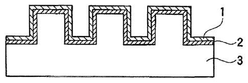
In a first embodiment of the present invention, as shown
in Fig. 1, a resin mold for imprinting having a three-layer
structure is provided which comprises a resin layer 3 having
a recessed and projected pattern surface, an inorganic material
layer 2 formed with a uniform thickness on at least the recessed
and projected pattern surface of the resin layer 3, and a release
agent layer 1 formed with a uniform thickness on at least the
recessed and projected pattern surface of the inorganic material
layer 2.
[0056]
In a second embodiment of the present invention, as shown
in Fig. 2, a resin mold for imprinting having a four-layer
structure is provided which comprises a substrate 4, a resin
layer 3 having a recessed and projected pattern surface that
is formed on the substrate, an inorganic material layer 2 formed
with a uniform thickness on at least the recessed and projected
pattern surface of the resin layer 3, and a release agent layer
1 formed with a uniform thickness on at least the recessed and
projected pattern surface of the inorganic material layer 2.
[0057]
Conventionally, the adhesion of a release agent onto a
resin layer was not good. In the present invention, however,
the provision of an inorganic material layer between the resin
CA 02768830 2012-01-20
SF-2278
layer and the release agent layer has enabled the formation with
good adhesion of the release agent layer onto the resin layer
through the inorganic material layer. Such formation has been
achieved as a result of good adhesion between the resin layer
5 and the inorganic material layer and good adhesion between the
inorganic material layer and the release agent layer.
Accordingly, the release agent layer is not peeled in imprinting,
enabling molding with good releasabilty. Furthermore, the
inorganic material layer has a thickness of not more than a
10 predetermined thickness, enabling the production of a flexible
mold.
[0058]
The first embodiment of the present invention and the
second embodiment of the present invention are related to each
15 other in such a manner that when the substrate is integrated
with the resin layer in the four-layer structure of the second
embodiment, this corresponds to the embodiment of the
three-layer structure of the first embodiment of the present
invention. The embodiment where the substrate is integrated
20 with the resin layer refers to an embodiment where the substrate
is a resin on which a pattern can be formed with a mold, in which
case the substrate represents a resin layer: in other words,
the substrate serves as a substrate and a resin layer.
[0059]
CA 02768830 2012-01-20
'SF-2278
21
1. Resin mold for imprinting
The first and the second embodiments of the present
invention each comprise a resin layer, an inorganic material
layer and a release agent layer as described below.
[0060]
(1) Resin layer having a recessed and projected pattern surface
(a) Resin
Resins forming the resin layer include thermoplastic
resins, thermosetting resins and photo-curable resins.
Preferred thermoplastic resins include acrylic resins, styrene
resins, olefin resins, polycarbonate resins, and polyester
resins. Preferred thermosetting resins or photo-curable resins
include epoxy resins. Further preferred examples include
polymethyl methacrylate, cycloolefin resins, styrene resins,
epoxy resins, polycarbonate, and polyethylene terephthalate.
[0061]
The aforementioned resins may contain components such as
antioxidants, photosensitizers, fillers and leveling agents in
a range which does not affect the nature of the aforementioned
resins.
[0062]
(b) Thickness
The resin layer has a thickness of usually 50nm to 30 pm,
preferably 500 nm to 10 pm.
CA 02768830 2012-01-20
SF-2278
22
[0063]
The resin layer having a thickness within the above range
has a strength resistant to stamping and a good smoothness and
thus can be handled easily.
[0064]
The thickness of the resin layer as used herein refers to
a distance between a bottom surface of the resin layer and the
highest surface of the recess and projected surface of the resin
layer.
[0065]
In the present invention, the thickness of the resin film
is usually 1 to 15 times, preferably 2 to 12 times, more
preferably 3 to 10 times the height of a recess and projection
formed on a surface of a master mold. Specifically, when the
thickness of the resin is defined as Y and the thickness of the
recess and projection is defined as X, as shown in Fig. 9, X
and Y are usually in the range of Y = X to Y = 15X, and preferably
in the range of Y = 2X to Y = 12X, more preferably in the range
of Y = 3X to Y = 10X. If the thickness of the resin film is less
than 1 time the height of the form, the height of the form of
the master mold is not reflected at a step such as in heat
imprinting during the preparation of the resin mold. If the
thickness of the resin film exceeds 15 times, in heat imprinting
during the preparation of the resin mold, a resin at the
CA 02768830 2012-01-20
SF-2278
23
transferred portion over-flows by pressing (which is carried
out usually at 20 MPa) , and the excess resin frequently forms
a projection at a side of the master mold. This makes it
difficult to form a resin mold having a uniform transfer surface.
The depth of a recess and projection formed on a master mold
is correlated with the resin thickness in such a manner as
described above, as a result of a considerably smaller depth
of a recess and projection employed in resin nanoimprinting in
the present invention than that in common-scale imprinting. If
Y is a large value, e.g., a value equal to 20X as adopted in
common printing technique, it is impossible to form a precise
resin replica mold for nanoimprinting.
[0066]
In the present invention, the resin thickness is an average
of thicknesses measured at arbitral five points of the surface
using a film thickness measurement instrument (model: F20,
manufactured by Filmmetrics, Inc. ) .
[0067]
(c) Surface
The resin layer has a desired form on the surface.
[0068]
The desired form is usually a recess and projection which
repeats itself in a predetermined cycle to form a pattern, i.e.,
a recess and projected pattern, preferably a recess and projected
CA 02768830 2012-01-20
F-2278
24
pattern having a cycle of 10 nm to 50 pm, a depth of 10 nm to
100 pm, and a transfer surface of 1.0 to 1.0 x 106mm2.
[0069]
Specific forms of the recess and projection include a line,
a column, a monolith, a cone, a polygonal pyramid and a microlens.
[0070]
(2) Inorganic material layer formed with a uniform thickness
on at least the recessed and projected pattern surface of the
resin layer
(a) Inorganic material
The inorganic material layer is formed from an inorganic
material or an inorganic oxide, preferably an inorganic oxide.
Preferred examples of the inorganic oxide include Si02, Zr02,
ZnO, Ta205, Hf02, ITO, FTO, and Ti02, and more preferred examples
thereof include Si02, Zr02, Ta205, Hf02, ITO, and TiO2. Preferred
examples of the inorganic material include Si and SiC.
[0071]
The use of the aforementioned inorganic materials as the
inorganic material layer improves the adhesion thereof with the
resin layer and the release agent layer.
[0072]
(b) Thickness
The thickness of the inorganic material layer is
preferably 0.5 to 100 nm, more preferably 0.5 to 20 nm, most
CA 02768830 2012-01-20
SF-2278
preferably 1 to 10 nm. When the thickness of the inorganic
material layer is within the above range, the imprinting can
be carried out with good precision and the adhesion thereof with
the resin layer and the release agent layer are good.
5 [0073]
(c) Surface
The inorganic material layer is formed with a uniform
thickness on the resin layer, at least on the recessed and
projected pattern surface of the resin layer. The uniform
10 thickness refers to a substantially uniform thickness, and
preferably a uniform thickess with a standard deviation of 0.1
to 15. Thus, the surface of the inorganic material layer retains
the form of the surface of the resin layer.
[0074]
15 (3) Release agent layer formed with a uniform thickness on at
least the recessed and projected pattern surface of the inorganic
material layer
(a) Release agent
A release agent is a component to decrease a surface energy
20 of a release surface and facilitate releasing.
[0075]
The release agent layer is preferably composed of at least
one kind selected from the group consisting of a fluorine-based
silane coupling agent, a perfluoro compound having an amino group
CA 02768830 2012-01-20
SF-2278
26
or a carboxyl group, and a perfluoroether compound having an
amino group or a carboxyl group; more preferably composed of
at least one kind selected from the group consisting of a
fluorine-based silane coupling agent having an amino group.
[0076]
The use of the aforementioned examples as the release agent
layer improves the adhesion thereof with the inorganic material
layer and the releasability thereof from a resin subjected to
imprinting.
[0077]
(b) Thickness
The thickness of the release agent layer is preferably 0.5
to 20 nm, more preferably 0.5 to 10 nm, most preferably 0.5 to
5 nm.
[0078]
(c) Surface
The release agent layer is formed with a uniform thickness
on the inorganic material layer, at least on the recessed and
projected pattern surface of the inorganic material layer. The
uniform thickness refers to a substantially uniform thickness,
and preferably a uniform thickess with a standard deviation of
0.1 to 10. Thus, the surface of the release agent layer retains
the form of the surface of the resin layer.
[0079]
CA 02768830 2012-01-20
SF-2278
27
(d) Property of the surface of the release agent layer
A contact angle of a release agent layer surface of the
release agent layer with respect to pure water is preferably
1000 or more, more preferably 100 to 1300, still more preferably
100 to 1200
.
[0080]
When the contact angle is within the above range, which
represents a low wetting property with respect to a liquid, in
the case where a surface of the release agent layer is coated
with a liquid resin to be subjected to imprinting, it is
considered that the resin can be prevented from being fluidized
on the surface of the release agent layer, and the resin subjected
to imprinting is readily released from the surface of the
release agent layer.
[0081]
(4) Substrate
In the four-layer structure embodiment of the present
invention, the resin layer is formed on a substrate.
[0082]
As the substrate, preferred is one type selected from the
group consisting of a resin, glass, silicon, sapphire, gallium
nitride, carbon and silicon carbide.
[0083]
As the resin employed for the substrate, preferred is one
CA 02768830 2012-01-20
'SF-2278
28
type selected from the group consisting of polyethylene
terephthalate, polycarbonate, polymethyl methacrylate,
polystyrene, cyclic polyolefin, polyimide, polysulfone,
polyether sulfone, and polyethylene naphthalate.
[0084]
As a form of the resin employed for the substrate, a plate
and a film can be mentioned. As a plate form, a polymethyl
methacrylate plate, a polycarbonate plate, a polycycloolefin
plate and the like can be mentioned; and as a film form, films
of polyethylene terephthalate, polycarbonate, cyclic
polyolefin, polyimide, polysulfone, polyether sulfone,
polyethylene naphthalate and the like can be mentioned, without
limiting thereto.
[0085]
(5) Surface form of the resin mold for imprinting of the present
invention
The surface form of the resin mold for imprinting of the
present invention is a recessed and projected pattern repeating
itself in a predetermine cycle.
[0086]
The pattern preferably has a cycle of 10 nm to 50 pm.
[0087]
A mold with a surface pattern form having a cycle of 20
nm to 500 nm is used suitably for semiconductor materials, media,
CA 02768830 2012-01-20
SF-2278
29
optical elements and the like. A mold with a surface pattern
form having a cycle of 200 nm to 20 pm is used suitably for optical
materials such as prisms and microlens.
[0088]
The pattern preferably has a depth of 50 nm to 1 pm, more
preferably 100 to 600 nm.
[0089]
Further, the transfer surface is preferably 1.0 to 0.25
x 106mm2.
[0090]
Specific forms of the recess and projection, which are not
particularly limited, include a line, a column, a monolith, a
cone, a polygonal pyramid and a microlens.
[0091]
(6) Roller type resin mold for imprinting
As an embodiment of the resin mold for imprinting of the
present invention, a roller type resin mold for imprinting can
be mentioned.
[0092]
In the roller type resin mold for imprinting, as shown in
Fig. 6, a mold having the same structure as that of the
aforementioned resin mold for imprinting is wound around a roller
or the like, with the recessed and projected surface facing
outside.
CA 02768830 2012-01-20
SF-2278
[0093]
The roller type resin mold for imprinting preferably has
a flexible structure in which the mold having three layers or
four layers has a thickness of 30 to 300 pm.
5 [0094]
2. Method for producing the resin mold for imprinting
A method for producing the resin mold for imprinting is
described with reference to Figures.
[0095]
10 In the Figures, the same marks are used for the same
structures as those in Figs. 1 and 2.
[0096]
A method for producing the resin mold for imprinting having
a three-layer structure is described with reference to Fig. 3.
15 [0097]
As shown in Fig. 3 (a), a substrate composed of a resin
is prepared as a resin layer 3.
[0098]
Then, as shown in Fig. 3 (b), by contacting a mold with
20 the resin layer 3, a recessed and projected pattern formed on
a surface of the mold is transferred on a surface of the resin
layer 3.
[0099]
Then, as shown in Fig. 3 (c), on at least a recessed and
CA 02768830 2012-01-20
SF-2278
31
projected pattern surface of the resin layer 3, an inorganic
material layer 2 with a uniform thickness is formed.
[0100]
Then, as shown in Fig. 3 (d), on at least a recessed and
projected pattern surface of the inorganic material layer 2,
a release agent layer 1 with a uniform thickness is formed,
thereby obtaining the resin mold for imprinting of the present
invention.
[0101]
A method for producing the resin mold for imprinting having
a four-layer structure is described with reference to Fig. 4.
[0102]
As shown in Fig. 4 (a), a substrate 4 is prepared.
[0103]
Then, as shown in Fig. 4 (b), on the substrate 4, a resin
layer 3 is formed.
[0104]
Then, as shown in Fig. 4 (c), by contacting a mold with
the resin layer 3, a recessed and projected pattern formed on
a surface of the mold is transferred on a surface of the resin
layer.
[0105]
Then, as shown in Fig. 4 (d), on at least a recessed and
projected pattern surface of the resin layer 3, an inorganic
CA 02768830 2012-01-20
SF-2278
32
material layer 2 with a uniform thickness is formed.
[0106]
Then, as shown in Fig. 4 (e), on at least a recessed and
projected pattern surface of the inorganic material layer 2,
a release agent layer 1 with a uniform thickness is formed.
[0107]
Each step will be described hereinafter. A material to
constitute each layer of the resin mold for imprinting is the
same as that described in the section of the resin mold for
imprinting as described above.
[0108]
<Step (I): a step of forming a resin layer on a substrate and/or
a step of contacting a mold with a resin layer so as to transfer
a recessed and projected pattern formed on a surface of the mold
onto a one-side surface of the resin layer>
(a) Formation of the resin layer
In the case of the resin mold for imprinting having a
three-layer structure, instead of the step of forming a resin
layer, a substrate composed of a resin is prepared as a resin
layer. At this time, preferred examples of the substrate
composed of a resin include polymethyl methacrylate,
polycarbonate and polycycloolefin, which have a suitable
hardness endurable to pressure.
[0109]
CA 02768830 2012-01-20
=
SF-2278
33
In the case of the resin mold for imprinting having a
four-layer structure, at first, a substrate is prepared. A
resin to form a resin layer on the substrate is optionally diluted
with an organic solvent or the like, and coated on the substrate
by means of e.g., spin coating, spray coating, bar coating, lip
coating, and slit coating. Then,
the coated resin is dried,
optionally using a hot plate or the like, thus forming a layer
having a thickness of preferably 50 nm to 30 pm, more preferably
50 nm to 10 pm.
[0110]
(b) Formation of form (pattern) on the resin layer surface
On the surface of the resin layer, a surface form (pattern)
of a mold, such as quartz, a metal and silicon, used for common
imprinting, is transferred (imprinted) . The surface form
(pattern) of the mold is not particularly limited, but preferably
has a cycle of 10 nm to 50 pm, a depth of 10 nm to 100 pm, a
transfer surface of 1.0 to 1.0 x 106mm2; more preferably has a
cycle of 20 nm to 20 pm, a depth of 50 nm to 1 pm, a transfer
surface of 1.0 to 0.25 x 106mm2, in which case sufficient pattern
can be formed on the resin layer.
[0111]
As transferring (imprinting) , when the resin layer is
composed of a thermoplastic resin or a thermosetting resin, heat
imprinting is carried out, and when the resin layer is composed
CA 02768830 2012-01-20
,
,
SF-2278
34
of a photo-curable resin, photo-imprinting is carried out.
[0112]
The heat imprinting can be performed through a common
operation employed for heat imprinting into thermoplastic resins
or thermosetting resins, but a preferred operation is, for
example, such that on a resin heated to a glass transition
temperature (Tg) or higher, a mold is pressed at a pressing
pressure of 0.5 to 50 MPa by retaining the mold for 10 to 600
seconds, and then the resin is cooled to a temperature of the
glass transition temperature (Tg) or lower, and the mold is
detached from the resin layer.
[0113]
The photo-imprinting can be performed through a common
operation employed for photo-imprinting into photo-curable
resins, but a preferred operation is, for example, such that
on the photo-curable resin, a mold is pressed at a pressing
pressure of 0.1 to 5 MPa by retaining the mold for 30 to 600
seconds, and ultraviolet ray is applied, and then the mold is
detached from the resin layer.
[0114]
<Step II: step of forming an inorganic material layer with a
uniform thickness on at least a recessed and projected pattern
surface of the resin layer>
On at least a surface form of the resin layer, a film of
CA 02768830 2012-01-20
SF-2278
an inorganic material or an inorganic oxide with a uniform
thickness having a thickness of preferably 0.5 to 100 nm, more
preferably 0.5 to 20 nm, most preferably 1 to 10 nm, is formed
by common film formation means such as the deposition or the
5 sputtering of an inorganic material or an inorganic oxide.
[0115]
<Step III: step of forming a release agent layer with a uniform
thickness on at least a recessed and projected pattern surface
of the inorganic material layer>
10 On at least a surface form of the inorganic material layer,
the release agent is coated by common means such as dip coating,
spin coating, deposition and spraying. The release agent may
be diluted with an organic solvent dissolving the release agent
before use.
15 [0116]
After the coating operation as described above, the
release agent coating surface is preferably subjected to rinsing
treatment using a fluorine-based solvent such as perfluorohexane
The rinsing treatment is preferred to provide the release agent
20 layer with a uniform thickness, but may not be carried out when
the release agent layer retains a uniform thickness in the
operation of coating the release agent.
[0117]
In this step, a release agent layer having a thickness of
CA 02768830 2012-01-20
SF-2278
36
preferably 0.5 to 20 nm, more preferably 0.5 to 10 nm, most
preferably 0.5 to 5 nm, is formed.
[0118]
3. Method for using the resin mold for imprinting
(1) Usual use method
The resin mold for imprinting of the present invention is
used suitably for the imprinting into a thermoplastic resin,
a thermosetting resin or a photo-curable resin; and more
preferably is used for the imprinting into a photo-curable resin_
An embodiment of a method for using the resin mold for imprinting
is described with reference to Fig. 5.
[0119]
As shown in Fig. 5 (a) , the resin mold for imprinting of
the present invention is contacted with a surface of a resin
5.
[0120]
Then, as shown in Fig. 5 (b) , the resin mold for imprinting
of the present invention is released, thereby obtaining a resin
5 provided with a form on the surface.
[0121]
<Step of contacting the resin mold for imprinting on a surface
of a resin>
The resin 5 to be subjected to imprinting is usually any
one of a thermoplastic resin, a thermosetting resin and a
CA 02768830 2012-01-20
SF-2278
37
photo-curable resin, and is usually present on a substrate 6.
[0122]
As the substrate 6, any substrate can be used without any
limitation as long as being employed for common imprinting, with
examples thereof including a resin, glass, silicon, sapphire,
gallium nitride, carbon and silicon carbide.
[0123]
When using thermoplastic resins or thermosetting resins,
a common operation employed for heat imprinting into
thermoplastic resins or thermosetting resins can be performed,
but an example of a preferred operation is such that the mold
is contacted, at a pressing pressure of 0.5 to 50 MPa, with a
resin heated to a glass transition temperature (Tg) or higher,
and the mold is pressed by retaining the mold for 10 to 600
seconds.
[0124]
When using photo-curable resins, a common operation
employed for photo-imprinting into photo-curable resins can be
performed, but an example of a preferred operation is such that
the mold is contacted with the resin at a pressing pressure of
0.1 to 5 MPa, and the mold is pressed by retaining the mold for
to 600 seconds, and then ultraviolet ray is applied.
[0125]
The photo-imprinting for the photo-curable resin does not
CA 02768830 2012-01-20
SF-2278
38
require a pressing pressure as large as that required in heat
imprinting, and thus, for the photo-imprinting into a
photo-curable resin, various embodiments of the resin mold for
imprinting of the present invention, for example, a flexible
embodiment, such as the resin mold for imprinting using a film
or the like as a substrate, can be used suitably.
[0126]
As the photo-curable resin, a common photo-curable resin
can be used without any limitation.
[0127]
<Step of releasing the resin mold for imprinting from a resin>
When using the thermoplastic resin or thermosetting resin,
the resin is cooled to a glass transition temperature (Tg) or
lower, and then the mold is pulled apart from the resin layer.
When using the photo-curable resin, the mold is pulled
apart from the resin layer.
[0128]
(2) Method for using a roller type resin mold for imprinting
The resin mold for imprinting of the present invention can
be used also as a roller type resin mold for imprinting, which
is used after the resin mold for imprinting is wound around a
roller or the like.
[0129]
The use of the roller type resin mold for imprinting is
CA 02768830 2012-01-20
SF-2278
39
suited for the imprinting into the photo-curable resin. As
shown in Fig. 6, in this use, the step of contacting the resin
mold for imprinting with the surface of the resin comprises the
steps of pressing the resin mold for imprinting, wound around
a roller, on the surface of the resin and applying an ultraviolet
ray.
[0130]
4. Use
The resin mold for imprinting of the present invention is
used for the imprinting into a thermoplastic resin, a
thermosetting resin, or a photo-curable resin.
[0131]
Individual products obtained from resins subjected to
imprinting can be used for a semiconductor material, an optical
element, a prism, a microlense, recording media, holography,
micro-machine, biology, environment, a semiconductor, a LED and
an electronic material such as a harddisk.
[0132]
When the resin mold for imprinting of the present invention
has a pattern form, on the surface, having a cycle of 20 nm to
500 nm, preferable uses are, for example, semiconductor
materials, media, and optical elements. When the resin mold for
imprinting of the present invention has a pattern form, on the
surface, having a cycle of 200 nm to 20 pm, preferable uses are,
CA 02768830 2012-01-20
SF-2278
for example, prisms and microlenses.
[0133]
When the resin mold for imprinting of the present invention
is a roller type resin mold for imprinting, continuous molding
5 is possible, and preferable uses are, for example, microlenses
and optical performance films such as anti-reflection films.
Examples
[0134]
10 The present invention will be described in detail with
reference to Examples, but the present invention shall not be
limited by these Examples.
[0135]
In the present specification and Examples, individual
15 values were measured by the following measurement methods.
[0136]
<Weight average molecular weight Mw>
The weight average molecular weight was obtained in terms
of standard polystyrene measured by gel permeation
20 chromatography (device: HLC-8220GPC manufactured by Toso
Corporation, solvent: tetrahydrofuran (THF)).
[0137]
<Thickness of a resin layer>
A distance between a bottom surface of the resin layer and
CA 02768830 2012-01-20
SF-2278
41
the highest surface of the recessed and proj ected pattern surface
of the resin layer was defined as a thickness of the resin layer.
[0138]
<Thickness of an inorganic material layer>
Arbitral five points of the surface were measured using
a film thickness measurement instrument (model: F20,
manufactured by Filmmetrics, Inc.) and an average of the measured
values was defined as a thickness of the oxide film layer. The
uniformity of the thickness was checked from the standard
deviation of the five points.
[0139]
<Thickness of a release agent layer>
Arbitral five points of the surface were measured using
a film thickness measurement instrument (model: 20,
manufactured by Filmmetrics, Inc.) and an average of the measured
values was defined as a thickness of the release agent layer.
The uniformity of the thickness was checked from the standard
deviation of the five points.
[0140]
<Contact angle of a surface of the release agent layer with
respect to pure water>
About 1 pL of a micro water droplet was placed still on
a surface of a specimen, and the specimen was subjected to
measurement in air using KYCWA CONTACT-ANGLE METER CA-D type
CA 02768830 2012-01-20
SF-2278
42
manufactured by Kyowa Interface Science Co., Ltd. The
measurement conditions were in accordance with JISR3257.
[0141]
A change ratio was calculated as follows:
(Contact angle of a release agent layer before imprinting -
Contact angle of a release agent layer after imprinting) /
Contact angle of a release agent layer before imprinting x 100
(%)
[0142]
<Surface form (pattern)
The cycle and line width were evaluated with SEM (S-4800
manufactured by Hitachi High-Technologies), and the depth
(height) was evaluated with AFM (L-trace manufactured by SII
Nano Technology Inc.).
[0143]
<Imprinting result>
Macro evaluation: a transfer surface formed on a resin
subjected to imprinting was observed with an optical microscope
(ELIPSE LV100 manufactured by Nicon Corporation) at a
magnification of 20, and the presence of the transfer-adhering
of the resin onto the mold was observed.
AA: resin transfer-adhering was absent.
BB: resin transfer-adhering was present.
SEM (cycle): a pattern formed on a resin subjected to
CA 02768830 2012-01-20
SF-2278
43
imprinting was evaluated with SEM, on the basis of a SEM
measurement result of a pattern formed on the surface of the
resin mold for imprinting, to see the presence of change under
the following criteria.
AA: a change ratio was less than 10 nm.
BB: a change ratio was not less than 10 nm.
AFM (depth): a pattern formed on a resin subjected to
imprinting was evaluated with AFM, on the basis of an AFM
measurement result of a pattern formed on the surface of the
resin mold for imprinting, to see the presence of change under
the following criteria.
AA: a change ratio was less than 10 nm.
BB: a change ratio was not less than 10 nm.
[Example 1]
(1) Production of a resin (preparation of a resin for a resin
mold (PMMA))
A flask equipped with a stirring device, a
nitrogen-introducing tube, a thermometer, and a reflux cooling
tube was charged with 100 parts by weight of methyl methacrylate
(product name: LIGHT ESTER M, manufactured by Kyoeisha Chemical
Co., Ltd.) and 100 parts by weight of toluene.
[0144]
Then, while introducing a nitrogen gas (0.3 L/min) into
the flask, the content in the flask was heated to 80 C, and 0.5
CA 02768830 2012-01-20
SF-2278
44
part by weight of dimethyl 2,2'-azobis(2-methylpropionate)
(product name: V-601, manufactured by Wako Pure Chemical
Industries, Ltd.) was added as an initiator. The mixture was
kept for 8.0 hours at 80 C.
[0145]
Then, the supply of the nitrogen gas was terminated, and
100 parts by weight of toluene was added thereby lowering the
temperature to terminate the reaction. A resin fora resin mold
(a resin fora resin layer (PMMA)) was thus obtained. A molecular
weight of the resin obtained is indicated in Table 1.
[0146]
(2) Formation of a resin layer (spin coating of the resin on
a substrate)
The resin for a resin mold (the resin for a resin layer
(PMMA)) obtained in (1) was diluted ten times with toluene, and
was spin coated on a polysulfone film (PSF) (product name:
SUMILITE71 FS-1200, manufactured by Sumitomo Bakelite Co., Ltd.,
thickness: 0.12 mm) substrate. Then, the coated resin was dried
at 130 C for 15 minutes using a hot plate, thereby preparing
a resin layer having a film thickness of 1.2 pm (the thickness
was 8 times as large as the height of the form of a master mold
to be used) on the substrate. A resin thickness was defined as
an average of thicknesses measured at arbitral five points of
the surface using a film thickness measurement instrument
CA 02768830 2012-01-20
SF-2278
(model: F20, manufactured by Filmmetrics, Inc. ) .
[0147]
(3) Formation of a pattern on a surface of the resin layer
Using ST-50 manufactured by Toshiba Machine Co., Ltd., the
5 laminate consisting of the film substrate and the resin layer
was heated to 140 C, and on a surface of the resin layer, a master
mold (a quarts mold which had been subjected to release treatment,
a transfer surface of 576 =2, 150 nmL/S, a cycle of 300 nm, a
depth of 150 nm, a linear form L/S (Line and Space) ) was pressed,
10 thereby carriing out heat imprinting at 140 C. The heat
imprinting was carried out at a pressing pressure of 20 MPa at
a retention time of 5 minutes. Then, the laminate was cooled
to a temperature of not higher than 80 C, and the master mold
was detached, thereby obtaining a resin layer having a pattern
15 formed on the one-side surface (transfer surface of 576 mm2, 150
nmL/S, a cycle of 300 nm, a depth of 150 nm) .
[0148]
(4) Formation of an inorganic material layer
On a surface on which the pattern was formed of the resin
20 layer
obtained in (3) , Si02 was deposited with the resin subjected
to rotation and revolution, thereby forming an oxide film coating
having a thickness of 3.8 nm serving as an inorganic material
layer. As the deposition, vacuum deposition was carried out at
room temperature for about 1 minute using an optical thin film
CA 02768830 2012-01-20
SF-2278
46
coater (OPTORUN OMC-1100). After the deposition, the surface
form of the inorganic material layer was visually observed to
have neither cracks nor defect.
[0149]
(5) Formation of a release agent layer
The laminate consisting of the inorganic material layer,
the resin layer and the substrate obtained in (4) was soaked
for 1 minute in a fluorine-based release agent liquid (product
name: OPTOOL HD-1100, manufactured by Daikin Industries, Ltd.),
took out from the liquid, and was allowed to stand still for
1 hour in humid heated environment of 70 C and 90%. Then, the
laminate was rinsed using a fluorine-based solvent (product
name: OPTOOL HD-TH, manufactured by Daikin Industries, Ltd.),
and was allowed to stand still for 24 hours in environment of
23 C and 65%. A resin mold for imprinting in which a release
agent layer was formed on the surface of the inorganic material
layer was thus obtained.
[0150]
The surface form of the release agent layer was observed
with SEM and AFM to have neither defect nor change (a line width
of 150 nm, a cycle of 300 rim, a depth of 150 nm, L/S). A contact
angle of the surface of the release agent layer obtained with
respect to pure water was measured and found to be 110 . Through
the above steps, a resin mold for imprinting as indicated in
CA 02768830 2012-01-20
SF-2278
47
Table 1 was produced.
[0151]
Using the resin mold for imprinting produced, the
following imprinting was carried out.
[0152]
(6) Imprinting using the resin mold for imprinting
On the resin mold for imprinting, 0.2 mL of a photo-curable
resin (product name: PAK-02, manufactured by Toyo Gosei Co.,
Ltd.) was dropped, and thereon, a polycarbonate film (product
name: LEXAN, manufactured by Asahi Glass Co., Ltd.) was placed.
Then, pressing was carried out at 0.4 MPa for 1 minute using
a photo-nanoimprinting device (manufactured by Engineerng
System Co . , Ltd.). Then, ultraviolet ray was applied (10 mW/cm2)
for 2 minutes. Then, the resin mold for imprinting was detached.
[0153]
Whether the resin mold for imprinting had a defect such
as the peeling of the release agent layer, after the imprinting,
was visually observed, and further, a contact angle was measured.
Further, a surface form of the resin subjected to imprinting
was observed with SEM and AFM, and was found to have a pattern
having a line width of 150 rim, a cycle of 300 rim, a depth of
150 rim, and L/S. The result is shown in the table as imprinting
result.
[0154]
CA 02768830 2012-01-20
SF-2278
48
Using the resin mold obtained, continuous
photo-imprinting of 20 shots was carried out. The imprinting
was achieved without any problem.
[0155]
[Example 2]
A resin mold for imprinting was prepared in the same manner
as in Example 1, except that in Example 1, (1) and (2) were not
carried out, and in (3) , using a polymethyl methacrylate (PMMA)
plate (product name: ACRYLITE EX, manufactured by Mitsubish
Rayon Co., Ltd., thickness: 3.0 mm) instead of using the laminate
consisting of the resin layer and the PSF film, heat imprinting
was carried out onto the surface of the PMMA plate at a heat
imprinting temperature of 160 C, at a pressing pressure of 5
MPa, and at a retention time of 30 seconds. Using the resin mold
for imprinting obtained, imprinting was carried out in the same
manner as in Example 1. The resin mold for imprinting obtained
and the result of the imprinting are shown in Table 5.
[0156]
Using the resin mold obtained, continuous
photo-imprinting of 20 shots was carried out. The imprinting
was achieved without any problem.
[0157]
[Example 3]
A resin mold for imprinting was prepared in the same manner
CA 02768830 2012-01-20
SF-2278
49
as in Example 1, except that in Exaple 1, the thickness of the
resin in (2) was 0.4 pm, and the master mold in (3) was changed
to a quarts mold which had been subjected to release treatment
(a transfer surface of 576 mm2, 25 nmL/S, a cycle of 50 nm, a
depth of 50 nm, a linear form L/S). Using the resin mold for
imprinting obtained, imprinting was carried out in the same
manner as in Example 1. The resin mold for imprinting obtained
and the result of the imprinting are shown in Table 1.
[0158]
Using the resin mold obtained, continuous
photo-imprinting of 20 shots was carried out. The imprinting
was achieved without any problem.
[0159]
[Example 4]
A resin mold for imprinting was prepared in the same manner
as in Example 1, except that in Example 1, the master mold in
(3) was changed to a quarts mold which had been subjected to
release treatment (a transfer surface of 576 mm2, 75 nmL/S, a
cycle of 150 nm, a depth of 150 nm, a linear form L/S). Using
the resin mold for imprinting obtained, imprinting was carried
out in the same manner as in Example 1. The resin mold for
imprinting obtained and the result of the imprinting are shown
in Table 1.
Using the resin mold obtained, continuous
CA 02768830 2012-01-20
SF-2278
photo-imprinting of 20 shots was carried out. The imprinting
was achieved without any problem.
[0160]
[Example 5]
5 A resin mold for imprinting was prepared in the same manner
as in Example 1, except that in Example 1, the master mold in
(3) was changed to a quarts mold which had been subjected to
release treatment (a transfer surface of 576 mm2, 10,000 nmL/S,
a cycle of 20,000 nm, a depth of 300 nm, a linear form L/S) .
10 Using the resin mold. for imprinting obtained, imprinting was
carried out in the same manner as in Example 1. The resin mold
for imprinting obtained and the result of the imprinting are
shown in Table 1.
[0161]
15 Using the resin mold obtained, continuous
photo-imprinting of 20 shots was carried out. The imprinting
was achieved without any problem.
[0162]
[Example 61
20 A resin mold for imprinting was prepared in the same manner
as in Example 1, except that in Example 1, the master mold in
(3) was changed to a quarts mold which had been subjected to
release treatment (a transfer surface of 576 mm2, a hole diameter
of 200 nm, a cycle of 400 nm, a depth of 200 nm, a column form) .
CA 02768830 2012-01-20
= =
SF-2278
51
Using the resin mold for imprinting obtained, imprinting was
carried out in the same manner as in Example 1. The resin mold
for imprinting obtained and the result of the imprinting are
shown in Table 1.
[0163]
Using the resin mold obtained, continuous
photo-imprinting of 20 shots was carried out. The imprinting
was achieved without any problem.
[0164]
[Example 7]
A resin mold for imprinting was prepared in the same manner
as in Example 1, except that in Example 1, the master mold in
(3) was changed to a quarts mold which had been subjected to
release treatment (a transfer surface of 576 mm2, a cycle of 300
nm, a depth of 300 nm, a moth eye form). Using the resin mold
for imprinting obtained, imprinting was carried out in the same
manner as in Example 1. The resin mold for imprinting obtained
and the result of the imprinting are shown in Table 1.
[0165]
Using the resin mold obtained, continuous
photo-imprinting of 20 shots was carried out. The imprinting
was achieved without any problem.
[0166]
[Example 8]
CA 02768830 2012-01-20
SF-2278
52
A resin mold for imprinting was prepared in the same manner
as in Example 1, except that in Example 1, the thickness of the
resin in (2) was 6.4 pm, and the master mold in (3) was changed
to a quarts mold which had been subjected to release treatment
(a transfer surface of 576 mm2, a hole diameter of 10,000 nm,
a cycle of 20,000 nm, a depth of 4,000 nm, a microlens form).
Using the resin mold for imprinting obtained, imprinting was
carried out in the same manner as in Example 1. The resin mold
for imprinting obtained and the result of the imprinting are
shown in Table 1.
[0167]
Using the resin mold obtained, continuous
photo-imprinting of 20 shots was carried out. The imprinting
was achieved without any problem.
[0168]
[Example 9]
A resin mold for imprinting was prepared in the same manner
as in Example 1, except that in (4) of Example 1, on the surface
of the resin layer, Zr02 was deposited instead of Si02 so as to
form a film of 3.2 nm serving as an inorganic material layer.
Using the resin mold for imprinting obtained, imprinting was
carried out in the same manner as in Example 1. The resin mold
for imprinting obtained and the result of the imprinting are
shown in Table 2.
CA 02768830 2012-01-20
SF-2278
53
[0169]
Using the resin mold obtained, continuous
photo-imprinting of 20 shots was carried out. The imprinting
was achieved without any problem.
[0170]
[Example 10]
A resin mold for imprinting was prepared in the same manner
as in Example 1, except that in (4) of Example 1, on the surface
of the resin layer, ITO was deposited instead of Si02 so as to
form a film of 2.8 nm serving as an inorganic material layer.
Using the resin mold for imprinting obtained, imprinting was
carried out in the same manner as in Example 1. The resin mold
for imprinting obtained and the result of the imprinting are
shown in Table 2.
[0171]
Using the resin mold obtained, continuous
photo-imprinting of 20 shots was carried out. The imprinting
was achieved without any problem.
[0172]
[Example 11]
A resin mold for imprinting was prepared in the same manner
as in Example 1, except that in (4) of Example 1, on the surface
of the resin layer, TiO2 was deposited instead of Si02 so as to
form a film of 2.2 nm serving as an inorganic material layer.
CA 02768830 2012-01-20
SF-2278
54
Using the resin mold for imprinting obtained, imprinting was
carried out in the same manner as in Example 1. The resin mold
for imprinting obtained and the result of the imprinting are
shown in Table 2.
[0173]
Using the resin mold obtained, continuous
photo-imprinting of 20 shots was carried out. The imprinting
was achieved without any problem.
[0174]
[Example 12]
A resin mold for imprinting was prepared in the same manner
as in Example 1, except that in (4) of Example 1, on the surface
of the resin layer, silicon, instead of Si02, was deposited at
room temperature by low-temperature film forming apparatus
(ICP-CVD) method with rotation and revolution, so as to form
an amorphous-silicon (a-Si) film serving as an inorganic
material layer. Using the resin mold for imprinting obtained,
imprinting was carried out in the same manner as in Example 1.
The resin mold for imprinting obtained and the result of the
imprinting are shown in Table 2.
[0175]
Using the resin mold obtained, continuous
photo-imprinting of 20 shots was carried out. The imprinting
was achieved without any problem.
CA 02768830 2012-01-20
SF-2278
[0176]
[Example 13]
A resin mold for imprinting was prepared in the same manner
as in Example 1, except that in (4) of Example 1, on the surface
5 of the resin layer, SiOx (a mixture wherein x is 1 to 5), instead
of Si02, was sputtered at room temperature with rotation and
revolution so as to forma coating film serving as an inorganic
material layer. Using the resin mold for imprinting obtained,
imprinting was carried out in the same manner as in Example 1.
10 The resin mold for imprinting obtained and the result of the
imprinting are shown in Table 2.
[0177]
Using the resin mold obtained, continuous
photo-imprinting of 20 shots was carried out. The imprinting
15 was achieved without any problem.
[0178]
[Example 14]
A resin mold for imprinting was prepared in the same manner
as in Example 1, except that in (4) of Example 1, on the surface
20 of the resin layer, Si02 and Zr02, instead of Si02, were
simultaneously sputtered at room temperature with rotation and
revolution so as to form a coating film serving as an inorganic
material layer. Using the resin mold for imprinting obtained,
imprinting was carried out in the same manner as in Example 1.
CA 02768830 2012-01-20
SF-2278
56
The resin mold for imprinting obtained and the result of the
imprinting are shown in Table 2.
[0179]
Using the resin mold obtained, continuous
photo-imprinting of 20 shots was carried out. The imprinting
was achieved without any problem.
[0180]
[Example 15]
A resin mold for imprinting was prepared in the same manner
as in Example 1, except that in (4) of Example 1, with rotation
and revolution, on the surface of the resin layer, Si02 was
deposited and then Zr02 was deposited so as to form an inorganic
material layer composed of two layers. Using the resin mold for
imprinting obtained, imprinting was carried out in the same
manner as in Example 1. The resin mold for imprinting obtained
and the result of the imprinting are shown in Table 2.
[0181]
Using the resin mold obtained, continuous
photo-imprinting of 20 shots was carried out. The imprinting
was achieved without any problem.
[0182]
[Example 16]
A resin mold for imprinting was prepared in the same manner
as in Example 1, except that in (5) of Example 1, the release
CA 02768830 2012-01-20
SF-2278
57
agent liquid was changed to
tridecafluoro(1,1,2,2)tetrahydrooctyl trichlorosilane.
Using the resin mold for imprinting obtained, imprinting was
carried out in the same manner as in Example 1. The resin mold
for imprinting obtained and the result of the imprinting are
shown in Table 3.
[0183]
Using the resin mold obtained, continuous
photo-imprinting of 20 shots was carried out. The imprinting
was achieved without any problem.
[0184]
[Example 17]
A resin mold for imprinting was prepared in the same manner
as in Example 1, except that in (5) of Example 1, the release
agent liquid was changed to perfluorohexanoic acid. Using the
resin mold for imprinting obtained, imprinting was carried out
in the same manner as in Example 1. The resin mold for imprinting
obtained and the result of the imprinting are shown in Table
3.
[0185]
Using the resin mold obtained, continuous
photo-imprinting of 20 shots was carried out. The imprinting
was achieved without any problem.
[0186]
CA 02768830 2012-01-20
SF-2278
58
[Example 18]
A resin mold for imprinting was prepared in the same manner
as in Example 1, except that in (5) of Example 1, the release
agent liquid was changed to 1H,1H-tridecafluoroheptylamine.
Using the resin mold for imprinting obtained, imprinting was
carried out in the same manner as in Example 1. The resin mold
for imprinting obtained and the result of the imprinting are
shown in Table 3.
[0187]
Using the resin mold obtained, continuous
photo-imprinting of 20 shots was carried out. The imprinting
was achieved without any problem.
[0188]
[Example 19]
A resin mold for imprinting was prepared in the same manner
as in Example 1, except that in (5) of Example 1, the release
agent liquid was changed to methyl triisocyanate silane (product
name: Orgatics ST-310, manufactured by Matsumoto Trading Co.,
Ltd.) . Using the resin mold for imprinting obtained, imprinting
was carried out in the same manner as in Example 1. The resin
mold for imprinting obtained and the result of the imprinting
are shown in Table 3.
[0189]
Using the resin mold obtained, continuous
CA 02768830 2012-01-20
SF-2278
59
photo-imprinting of 20 shots was carried out. The imprinting
was achieved without any problem.
[0190]
[Example 20]
A resin mold for imprinting was prepared in the same manner
as in Example 1, except that in (1) of Example 1, 100 parts by
weight of methyl methacrylate was replaced by 100 parts by weight
of styrene (product name: styrene monomer, manufactured by
Idemitsu Kosan Co., Ltd.) . Using the resin mold for imprinting
obtained, imprinting was carried out in the same manner as in
Example 1. The resin mold for imprinting obtained and the result
of the imprinting are shown in Table 4.
[0191]
Using the resin mold obtained, continuous
photo-imprinting of 20 shots was carried out. The imprinting
was achieved without any problem.
[0192]
[Example 21]
Instead of carrying out (1) and (2) of Example 1, the
following operation was carried out to prepare a laminate
consisting of a resin layer and a substrate.
[0193]
Into 100 parts by weight of an epoxy resin (product name:
OGSOL EG, manufactured by Osaka Gas Chemicals Co., Ltd. ) , 5 parts
CA 02768830 2012-01-20
SF-2278
by weight of an acid anhydride based curing agent (product name:
RIKACID MH-700, manufactured by New Japan Chemical Co., Ltd.)
was added, and the mixture was sufficiently stirred to form a
composition. The composition was diluted ten times with toluene,
5 and was spin coated on a polysulfone film (PSF) (product name:
SUMILITETm FS-1200, manufactured by Sumitomo Bakelite Co., Ltd.,
thickness: 0.12 mm) substrate. Then, the laminate obtained was
heated at 140 C for 3 hours using a hot plate, thereby curing
the epoxy resin to provide a laminate consisting of the substrate
10 and the resin layer.
[0194]
A resin mold for imprinting was prepared in the same manner
as in (3) to (5) of Example 1, except that the above laminate
consisting of the substrate and the resin layer was used. Using
15 the resin mold for imprinting obtained, imprinting was carried
out in the same manner as in Example 1. The resin mold for
imprinting obtained and the result of the imprinting are shown
in Table 4.
[0195]
20 Using the resin mold obtained, continuous
photo-imprinting of 20 shots was carried out. The imprinting
was achieved without any problem.
[0196]
[Example 22]
CA 02768830 2012-01-20
SF-2278
61
Instead of carrying out (1) to (3) of Example 1, the
following operation was carried out to prepare a laminate
consisting of a resin layer having a pattern form on the surface
and a substrate.
[0197]
An acrylic based photo-curable resin PAK-02 (manufactured
by Toyo Gosei Co., Ltd.) was spin coated on a polysulfone film
(product name: SUMILITETm FS-1200, manufactured by Sumitomo
Bakelite Co., Ltd. ) .
[0198]
On a surface of the resin on the film substrate, a master
mold (a quarts mold which had been subjected to release treatment,
a transfer surface of 576 mm2, 150 nmL/S, a cycle of 300 nm, a
depth of 150 nm) was pressed at 0.4 MPa for 1 minute using a
photo-nanoimprinting device (manufactured by Engineerng System
Co., Ltd.) . This was followed by the application of ultraviolet
ray (10 mW/cm2) for 2 minutes. Then, the quartz mold was detached,
thereby obtaining a resin layer having a pattern formed on the
one-side surface (transfer surface of 576 mm2, 150 nmL/S, a cycle
of 300 nm, a depth of 150 nm) .
[0199]
A resin mold for imprinting was prepared in the same manner
as in (4) to (5) of Example 1, except that the above resin layer
having a pattern form on the surface was used. Using the resin
CA 02768830 2012-01-20
SF-2278
62
mold for imprinting obtained, imprinting was carried out in the
same manner as in Example 1. The resin mold for imprinting
obtained and the result of the imprinting are shown in Table
4.
[0200]
Using the resin mold obtained, continuous
photo-imprinting of 20 shots was carried out. The imprinting
was achieved without any problem.
[0201]
[Example 23]
A resin mold for imprinting was prepared in the same manner
as in Example 1, except that (1) and (2) of Example I were not
carried out, and a cycloolefin polymer (COP) plate (product name:
ZEONEX 2T, manufactured by Zeon Corporation, thickness: 2 mm)
was a substitute for the laminate consisting of the resin layer
and the substrate, and further in (3) of Example 1, heat
imprinting was carried out on the surface of the cycloolefin
polymer plate at a heat imprinting temperature of 150 C, at a
pressing pressure of 5 MPa, and at a retention time of 30 seconds.
Using the resin mold for imprinting obtained, imprinting was
carried out in the same manner as in Example 1. The resin mold
for imprinting obtained and the result of the imprinting are
shown in Table 5.
[0202]
CA 02768830 2012-01-20
SF-2278
63
Using the resin mold obtained, continuous
photo-imprinting of 20 shots was carried out. The imprinting
was achieved without any problem.
[0203]
[Example 24]
A resin mold for imprinting was prepared in the same manner
as in Example 1, except that (1) and (2) of Example 1 were not
carried out, and a polycarbonate (PC) film (product name: LEXAN,
manufactured by Asahi Glass Co., Ltd., thickness: 1 mm) was a
substitute for the laminate consisting of the resin layer and
the substrate, and further in (3) of Example 1, heat imprinting
was carried out on the surface of the polycarbonate film at a
heat imprinting temperature of 170 C, at a pressing pressure
of 5 MPa, and at a retention time of 30 seconds. Using the resin
mold for imprinting obtained, imprinting was carried out in the
same manner as in Example 1. The resin mold for imprinting
obtained and the result of the imprinting are shown in Table
5.
[0204]
Using the resin mold obtained, continuous
photo-imprinting of 20 shots was carried out. The imprinting
was achieved without any problem.
[0205]
[Example 25]
CA 02768830 2012-05-07
72932-352
64
A resin mold for imprinting was prepared in the same manner
as in Example 1, except that (1) and (2) of Example 1 were not
carried out, and a polyethylene terephthalate (PET) film
(product name: TeijinTM Tetron TM film, manufactured by Teij in
Limited, thickness: 0.1 mm) was a substitute for the laminate
consisting of the resin layer and the substrate, and further
in (3) of Example 1, heat imprinting was carried out on the
surface of the polyethylene terephthalate film at a heat imprinting
. temperature of 170 C, at a pressing pressure of 5 MPa, and at
a retention time of 30 seconds. Using the resin mold for
imprinting obtained, imprinting was carried out in the same
manner as in Example 1. The resin mold for imprinting obtained
and the result of the imprinting are shown in Table 5.
[0206]
Using the resin mold obtained, continuous
photo-imprinting of 20 shots was carried out. The imprinting
was achieved without any problem.
[0207]
[Example 26]
A resin mold for imprinting was prepared in the same manner
as in Example 1, except that in (2) of Example 1, the substrate
was changed from the polysulfone film to soda glass (manufactured
by Asahi Glass Co., Ltd., thickness: 1.1 mm) . Using the resin
mold for imprinting obtained, imprinting was carried out in the
CA 02768830 2012-01-20
SF-2278
same manner as in Example 1. The resin mold for imprinting
obtained and the result of the imprinting are shown in Table
6.
[0208]
5 Using the
resin mold obtained, continuous
photo-imprinting of 20 shots was carried out. The imprinting
was achieved without any problem.
[0209]
[Example 27]
10 A resin
mold for imprinting was prepared in the same manner
as in Example 1, except that in (2) of Example 1, the substrate
was changed from the polysulfone film to a silicon wafer
(manufactured by Covalent Materials Corporation, grade used:
polished wafer, thickness: 0.5 mm). Using the resin mold for
15 imprinting obtained, imprinting was carried out in the same
manner as in Example 1. The resin mold for imprinting obtained
and the result of the imprinting are shown in Table 6.
[0210]
Using the resin mold obtained, continuous
20 photo-
imprinting of 20 shots was carried out. The imprinting
was achieved without any problem.
[0211]
[Example 28]
A resin mold for imprinting was prepared in the same manner
CA 02768830 2012-01-20
SF-2278
66
as in Example 1, except that in (2) of Example 1, the substrate
was changed from the polysulfone film to a sapphire substrate
(manufactured by ORBE PIONEER LTD., semiconductor grade,
thickness: 0.5 mm) . Using the resin mold for imprinting
obtained, imprinting was carried out in the same manner as in
Example 1. The resin mold for imprinting obtained and the result
of the imprinting are shown in Table 6.
[0212]
Using the resin mold obtained, continuous
photo-imprinting of 20 shots was carried out. The imprinting
was achieved without any problem.
[0213]
[Example 29]
A resin mold for imprinting was prepared in the same manner
as in Example 1, except that in (2) of Example 1, the substrate
was changed from the polysulfone film to a gallium nitride
substrate (manufactured by Sumitomo Electric Industries, Ltd.,
one-side specular finishing, thickness: 0.4 mm) . Using the
resin mold for imprinting obtained, imprinting was carried out
in the same manner as in Example 1. The resin mold for imprinting
obtained and the result of the imprinting are shown in Table
6.
[0214]
Using the resin mold obtained, continuous
CA 02768830 2012-01-20
SF-2278
67
photo-imprinting of 20 shots was carried out. The imprinting
was achieved without any problem.
[0215]
[Example 30]
A resin mold for imprinting was prepared in the same manner
as in Example 1, except that in (2) of Example 1, the substrate
was changed from the polysulfone film to a polyethylene
terephthalate (PET) film (product name: TeijiilTM Tetron TM film,
manufactured by Teij in Limited, thickness: 0.1 mm) . Using the
resin mold for imprinting obtained, imprinting was carried out
in the same manner as in Example 1. The resin mold for imprinting
obtained and the result of the imprinting are shown in Table
6.
[0216]
Using the resin mold obtained, continuous
photo-imprinting of 20 shots was carried out. The imprinting
was achieved without any problem.
[0217]
[Example 31]
A resin mold for imprinting was prepared in the same manner
as in Example 1, except that in (2) of Example 1, the substrate
was changed from the polysulfone film to a polycarbonate (PC)
film (product name: LEXAN, manufactured by Asahi Glass Co., Ltd.,
thickness: 0.12 mm) . Using the resin mold for imprinting
CA 02768830 2012-01-20
SF-2278
68
obtained, imprinting was carried out in the same manner as in
Example 1. The resin mold for imprinting obtained and the result
of the imprinting are shown in Table 6.
[0218]
Using the resin mold obtained, continuous
photo-imprinting of 20 shots was carried out. The imprinting
was achieved without any problem.
[0219]
[Example 32]
A resin mold for imprinting was prepared in the same manner
as in Example 1, except that in (2) of Example 1, the substrate
was changed from the polysulfone film to a polyethylene
naphthalate (PEN) film (product name: Teonex, manufactured by
Teijin Chemicals Limited, thickness: 0.12 mm). Using the resin
mold for imprinting obtained, imprinting was carried out in the
same manner as in Example 1. The resin mold for imprinting
obtained and the result of the imprinting are shown in Table
6.
[0220]
Using the resin mold obtained, continuous
photo-imprinting of 20 shots was carried out. The imprinting
was achieved without any problem.
[0221]
[Example 33]
CA 02768830 2012-01-20
SF-2278
69
A resin mold for imprinting was prepared in the same manner
as in Example 1, except that in (2) of Example 1, the substrate
was changed from the polysulfone film to a polyimide film
(product name: AURUM film, manufactured by Mitsui Chemicals,
Inc., thickness: 0.3 mm) . Using the resin mold for imprinting
obtained, imprinting was carried out in the same manner as in
Example 1. The resin mold for imprinting obtained and the result
of the imprinting are shown in Table 6.
[0222]
Using the resin mold obtained, continuous
photo-imprinting of 20 shots was carried out. The imprinting
was achieved without any problem.
[0223]
[Example 34]
A resin mold for imprinting was prepared in the same manner
as in Example 1, except that in (2) of Example 1, the substrate
was changed from the polysulfone film to a polymethyl
methacrylate (PMMA) film (product name: ACRYPLEN, manufactured
by Mitsuibishi Rayon Co., Ltd., thickness: 0.12 mm) . Using the
resin mold for imprinting obtained, imprinting was carried out
in the same manner as in Example 1. The resin mold for imprinting
obtained and the result of the imprinting are shown in Table
6.
[0224]
CA 02768830 2012-01-20
SF-2278
Using the resin mold obtained, continuous
photo-imprinting of 20 shots was carried out. The imprinting
was achieved without any problem.
[0225]
5 [Example 35]
A resin mold for imprinting was prepared in the same manner
as in Example 1, except that in (2) of Example 1, the substrate
was changed from the polysulfone film to glassy carbon (GC)
(grade: SA-1, manufactured by Tokai Carbon Co., Ltd., thickness:
10 1.0 mm) .
Using the resin mold for imprinting obtained,
imprinting was carried out in the same manner as in Example 1.
The resin mold for imprinting obtained and the result of the
imprinting are shown in Table 6.
[0226]
15 Using the
resin mold obtained, continuous
photo-imprinting of 20 shots was carried out. The imprinting
was achieved without any problem.
[0227]
[Example 36]
20 A resin
mold for imprinting was prepared in the same manner
as in Example 1, except that in (2) of Example 1, the substrate
was changed from the polysulfone film to a silicon carbide (SiC)
wafer (grade: 6H N-type, manufactured by TankeBlue Semiconductor
Co., Ltd., thickness: 0.43 mm) . Using
the resin mold for
CA 02768830 2012-01-20
SF-2278
71
imprinting obtained, imprinting was carried out in the same
manner as in Example 1. The resin mold for imprinting obtained
and the result of the imprinting are shown in Table 6.
[0228]
Using the resin mold obtained, continuous
photo-imprinting of 20 shots was carried out. The imprinting
was achieved without any problem.
[0229]
[Example 37]
A resin mold for imprinting was prepared in the same manner
as in Example 1, except that in (2) of Example 1, the substrate
was changed from the polysulfone film to a polymethyl
methacrylate film (product name: ACRYPLEN, manufactured by
Mitsuibishi Rayon Co., Ltd., thickness: 0.12 mm). Using the
resin mold for imprinting obtained, imprinting was carried out
in the same manner as in Example 1. The resin mold for imprinting
obtained and the result of the imprinting are shown in Table
6.
[0230]
Using the resin mold obtained, continuous
photo-imprinting of 20 shots was carried out. The imprinting
was achieved without any problem.
[0231]
[Example 38]
CA 02768830 2012-01-20
SF-2278
72
A resin mold for imprinting was prepared in the same manner
as in Example 1, except that in (2) of Example 1, the substrate
was changed from the polysulfone film to a PET (polyethylene
terephthalate) film (product name: TeijinTm Tetron TM film,
manufactured by Teij in Limited, thickness: 0.25 mm) . Using the
resin mold for imprinting obtained, imprinting was carried out
in the same manner as in Example 1. The resin mold for imprinting
obtained and the result of the imprinting are shown in Table
6.
[0232]
Using the resin mold obtained, continuous
photo-imprinting of 20 shots was carried out. The imprinting
was achieved without any problem.
[0233]
[Example 391
Using the resin mold for imprinting of Example 1,
imprinting was carried out as follows instead of carrying out
(6) of Example 1.
[0234]
As a resin for a resin layer, a commercial cyclohexyl
methacrylate (CHMA) (product name: LIGHT ESTER CH, manufactured
by Kyoeisha Chemical Co., Ltd.) was spin coated on a glass
substrate to form a laminate consisting of the substrate and
the resin. The laminate was heated to 130 C, thereby preparing
CA 02768830 2012-01-20
SF-2278
73
a resin layer to be subjected to imprinting.
[0235]
On the surface of the resin layer to be subjected to
imprinting, the resin mold for imprinting (a transfer surface
of 576=12, 150 nmL/S) prepared in Example 1 was pressed, thereby
carrying out heat imprinting at 100 C. In the heat imprinting,
the pressing pressure was 20 MPa, and the retention time was
5 minutes. Then, the laminate consisting of the resin layer
subjected to imprinting and the substrate was cooled to a
temperature of not higher than 80 C, and the resin mold was
detached. The presence of the peeling or the like of the release
agent layer of the resin mold for imprinting, after imprinting,
was visually observed, and a contact angle was meausured. The
surface form of the resin subjected to imprinting was observed
with SEM and AFM, and was found to have a pattern having a line
width of 150 nm, a cycle of 300 nm, and a depth of 150 nm.
The result is shown in Table 7 as imprinting result.
[0236]
Using the resin mold obtained, continuous
photo-imprinting of 20 shots was carried out. The imprinting
was achieved without any problem.
[0237]
[Example 40]
Using the resin mold for imprinting of Example 1,
CA 02768830 2012-01-20
,
SF-2278
74
imprinting was carried out as follows instead of carrying out
(6) of Example 1.
[0238]
The resin mold for imprinting obtained in Example 1 was
wound around a roll of 6 inches in diameter, and the roll was
pressed at 1.0 MPa on a polycarbonate film (LEXAN film,
thickness: 0.12 mm, manufactured by Asahi Glass Co., Ltd.) coated
with a photo-curable resin (product name: PAK-02, manufactured
by Toyo Gosei Co., Ltd.), and at such a state, a line was moved
(a moving rate of 1 m/min). Then, while moving the line,
ultraviolet ray was applied (70 mW/cm2) to cure the resin. Then,
the resin mold for imprinting was detached from the roll, and
was found to have no defect such as the peeling of the release
agent layer.
[0239]
Along with the visual observation after imprinting of
whether the resin mold for imprinting had any defect such as
the peeling of the release agent layer, a contact angle was
measured. Meanwhile, a surface form of the resin subjected to
imprinting was observed with SEM and AFM, and was found to have
a pattern having a line width of 150 nm, a cycle of 300 nm and
a depth of 150 nm. The result is shown in Table 7 as imprinting
result.
[0240]
CA 02768830 2012-01-20
,
,
SF-2278
[Comparative Example 1]
(1) to (3) of Example 1 were carried out, thereby preparing
a resin mold for imprinting formed from a substrate and a resin
layer. Using the resin mold for imprinting obtained, imprinting
5 was carried out in the same manner as in Example 1. The resin
mold for imprinting obtained and the result of the imprinting
are shown in Table 8.
[0241]
[Comparative Example 2]
10 (1)
to (3) and (5) of Example 1 were carried out, thereby
preparing a resin mold for imprinting formed from a substrate,
a resin layer, and a release agent layer. Using the resin mold
for imprinting obtained, imprinting was carried out in the same
manner as in Example 1. The resin mold for imprinting obtained
15 and the result of the imprinting are shown in Table 8.
[0242]
[Comparative Example 3]
(1) to (4) of Example 1 were carried out, thereby preparing
a resin mold for imprinting formed from a substrate, a resin
20 layer, and an inorganic material layer. Using the resin mold
for imprinting obtained, imprinting was carried out in the same
manner as in Example 1. The resin mold for imprinting obtained
and the result of the imprinting are shown in Table 8.
[0243]
CA 02768830 2012-01-20
SF-2278
76
[Comparative Example 4]
In (1) of Example 1, 40 parts by weight of methyl
methacrylate was replaced by 40 parts by weight of perflorooctyl
ethyl methacrylate (product name: LIGHT ESTER FM-108,
manufactured by Kyoeisha Chemical Co., Ltd. ) , thereby producing
a resin for a resin layer. Then, the same operation as in (2)
and (3) of Example 1 was carried out. (4) and (5) of Example
1 were not carried out. A resin mold for imprinting formed from
a substrate and a resin layer was thus prepared. Using the resin
mold for imprinting obtained, imprinting was carried out in the
same manner as in Example 1. The resin mold for imprinting
obtained and the result of the imprinting are shown in Table
8.
[0244]
[Comparative Example 5]
In (1) of Example 1, 40 parts by weight of methyl
methacrylate was replaced by 40 parts by weight of perflorooctyl
ethyl methacrylate (product name LIGHT ESTER FM-108,
manufactured by Kyoeisha Chemical Co., Ltd. ) , thereby producing
a resin for a resin layer. Then, the same operation as in (2)
and (3) of Example 1 was carried out. Then, (4) of Example 1
was not carried out, and (5) of Example 1 was carried out. A
resin mold for imprinting formed from a substrate, a resin layer
and a release agent layer was thus prepared. Using the resin
CA 02768830 2012-01-20
SF-2278
77
mold for imprinting obtained, imprinting was carried out in the
same manner as in Example 1. The resin mold for imprinting
obtained and the result of the imprinting are shown in Table
8.
[0245]
[Reference Example 1]
A resin mold for imprinting was prepared in the same manner
as in Example 1, except that in (4) of Example 1, the thickness
of the Si02 film layer was changed to 120 nm. Using the resin
mold for imprinting obtained, imprinting was carried out in the
same manner as in Example 1. As a result, because of the too
large thickness of the inorganic material layer, a crack occurred
in the deposition in (4). A resin subjected to imprinting had
a form reflecting the crack. The resin mold for imprinting
obtained and the result of the imprinting are shown in Table
9.
[0246]
[Reference Example 2]
A resin mold for imprinting was prepared in the same manner
as in Example 1, except that in (4) of Example 1, the thickness
of the Si02 film layer was changed to less than 0.5 nm. Using
the resin mold for imprinting obtained, imprinting was carried
out in the same manner as in Example 1.
[0247]
CA 02768830 2012-01-20
SF-2278
78
However, because of the too small thickness of the
inorganic material layer, the adhesion was not sufficiently
retained between the release agent layer formed on the inorganic
material layer and the film of the inorganic material layer,
increasing the occurrence rate of the micro peeling of the
release agent and lowering the imprinting precision.
[0248]
The resin mold for imprinting obtained and the result of
the imprinting are shown in Table 9.
[0249]
The thickness of the Si02 film layer was too small to
measure, and thus is a calculated value in view of the deposition
conditions.
[0250]
[Reference Example 3]
A resin mold for imprinting was prepared in the same manner
as in Example 1, except that in (5) of Example 1, the thickness
of the release agent layer was changed to 21.4 nm. As a result,
because of the too large thickness of the release agent layer,
there was a change in a pattern form of a resin mold for imprinting
obtained (a line width of 160 nm, a cycle of 300 nm, and a depth
of 150 nm) relative to the pattern form of the master mold. Using
the resin mold for imprinting obtained, imprinting was carried
out in the same manner as in Example 1. The resin mold for
CA 02768830 2012-01-20
SF-2278
79
imprinting obtained and the result of the imprinting are shown
in Table 9.
[0251]
Using the resin mold obtained, continuous
photo-imprinting of 20 shots was carried out. The imprinting
was achieved without any problem.
[0252]
However, the surface of the resin subjected to imprinting,
when analyzed with FT-IR, was found to have the release agent
transferred thereto, presumably because of the too large
thickness of the release agent layer.
[0253]
[Reference Example 4]
A resin mold for imprinting was prepared in the same manner
as in Example 1, except that in (5) of Example 1, the thickness
of the release agent layer was changed to less than 0.5 nm. Using
the resin mold for imprinting obtained, imprinting was carried
out in the same manner as in Example 1. As a result, the too
small thickness of the release agent layer decreased the resin
releasing efficiency.
[0254]
The resin mold for imprinting obtained and the result of
the imprinting are shown in Table 9.
[0255]
CA 02768830 2012-01-20
,
,
SF-2278
The thickness of the release agent layer was too small to
measure, and thus is a calculated value in view of the treatment
conditions.
[0256]
5 [Table 1]
,
-,l
ND
l0
W
Table 1 Differnece in Mold Form
Iv
1
c).)
Ex.1 Ex.3 Ex.4 Ex. 5 Ex. 6 Ex. 7 Ex. 8 (xi
Type PSF PSF PSF PSF
PSF PSF PSF i\>
Substrate
Thickness (mm) 0.12 0.12 0.12 0.12 0.12 0.12 0.12
Type
PMMA PMMA PMMA PMMA PMMA PMMA PMMA
esi
Rn
Thickness (}lm) 1.2 0.4 1.2 1.2 1.2 1.2 6.4
layer
Weight average molecular weight (Mw)(x104) 8.3 8.3 8.3 8.3 8.3
8.3 8.3
Inorganic Film material Si02 Si02 Si02 Si02
Si02 Si02 Si02
material Thickness (nm) 3.8 3.2 2.6 4.6
3.8 3.2 2.6
layer Standard deviation of thickness 0.75 0.75
0.49 0.49 0.75 0.75 0.49
Release agent HD-
1100 HD-1100 HD-1100 HD-1100 HD-1100 HD-1100 HD-1100 0
Thickness (nm) 3.2 4.6 3.2 2.8 3.2 4.6 3.2 0
IV
Standard deviation of thickness 0.75 0.49 0.98 0.40
0.75 0.49 0.98 --I
0
Release
0
Contact angle Before imprinting ( ) 110 110 110
110 110 110 110 0
u.)
agent with respect to After imprinting ( ) 108 110
110 110 108 110 110 co 0
1--,
layer
waterIV
Change ratio (%) between
0
1-`
before and after 1.8 0.0 0.0 0.0
1.8 0.0 0.0 -,
i
0
imprintings
rs)
i
Pattern cycle of Master mold used (nm) 300 50 150 20,000
400 300 20,000 0
ko
Form of Master mold used L/S L/S L/S L/S column moth
eye lens
Macro evaluation M AA AA AA AA
AA AA
Imprinting result SEM (cycle) AA AA M AA
AA AA AA
AFM (depth) AA AA AA AA AA AA AA
[ 0 2 57 ]
[Table 2] .
--.1
N.)
(:)
w
N)
1
Table 2 Difference in Inorganic Material Layer w
,
,\)
Ex.1 Ex,9 Ex.10 Ex, 11 Ex. 12 Ex, 13 Ex. 14 Ex.15
Type PSF PSF PSF PSF PSF
PSF PSF PSF
Substrate
Thickness (mm) 0.12 0.12 0.12 0.12 0.12 0.12 0.12
0.12
,
Type
PMMA PMMA PMMA PMMA PMMA PMMA PMMA PMMA
Resin
Thickness (pm) 1.2 1.2 1.2 1.2 1,2 1.2 1,2 1.2
layer
Weight average molecular weight (Mw)(x104) 8.3 8.3 8.3 8.3
8,3 8.3 8.3 8.3
Inorganic Film material S102 Zr02 ITO TiO2 Si
SiO, Si02/ Zr02 S1021 Zr02
material Thickness (nm) 3.8 3.2 2.8 2.2 3.4
4.8 4.8 4.2 _
layer Standard deviation of thickness 0.75
0.98 0.40 0,40 0.80 0.49 0.57 0.57 0
Release agent HD-1100 HD-
1100 HD-1100 HD-1100 HD-1100 HD-1100 HD-1100 HD-1100 0
N.,
Thickness (nm) 3,2 3.2 2.8 2.2 3.4 2.8 3.2
2.8 -,
0,
0
Standard deviation of thickness 0.75 0.98 0.40 0,40
0.80 0.40 0.45 0.58 00
w
Release
Contact angle Before imprinting ( 0*) 110 110
110 110 110 110 110 110 00
agent with respect After imprinting ( ) 108 106 106 106
106 106 106 106 0
H
laYer to water Change ratio (%) between
..,
,
before and after 1.8 3.6 3.6 3.6 3.6
3.6 3.6 3.6 0
N.,
,
imprintings 0
0
Pattern cycle of Master mold used (nm) 300 300 300 300 300
300 300 300
Form of Master mold used [IS L/S L/S L/S US US L/S
L/S
Macro evaluation AA AA AA AA AA AA
AA AA
Imprinting result SEM (cycle) M AA AA AA AA
AA AA AA
AFM (depth) AA AA AA AA AA AA AA AA
[0258]
[Table 3]
=
-]
N)
w
N)
Table 3 Type of Release Agent
1
u.)
Ex.1 Ex.16 Ex.17 Ex. 18 Ex. 19
m
Substrate Type PSF PSF PSF PSF PSF
Thickness (mm) 0.12 0.12 0.12 0.12 0.12
Type PMMA PMMA PMMA PMMA PMMA _
Resin
Thickness (pm) 1.2 1.2 1.2 1.2 1.2
layer
Weight average molecular weight (Mw)(x104) 8.3 8.3 8.3 8.3 8.3
Inorganic Film material S102 Si02 S102 Si02
Si02
material Thickness (nm) 3.8 3.2 2,6 4.6
3.2
layer Standard deviation of thickness 0.75
0.75 0.49 0.49 0.98 0
Release agent HD-1100 A B C D
>
Thickness (nm) 3.2 3.4 4.6 . 3.2 2.6
0
N.)
-4
Standard deviation of thickness 0.75 0.80
0.49 0.75 0.49 0,
Release
0
Contact angle Before imprinting ( ) 110 110 110 110
103 m
w
00
0
agent with respect After imprinting ( e ) 108 106
108 108 101 w
layer
i.,
to water Change ratio (%) between
0
,
before and after 1.8 3.6 1.8 1.8
1.9 ..,
1
0
imprintings "
i
Pattern cycle of Master mold used (nm) 300
300 300 300 300 0
0
Form of Master mold used L/S L/S US L/S L/S
Macro evaluation AA AA AA AA AA
Imprinting result SEM (cycle) AA AA AA AA
AA
AFM (depth) AA AA AA AA AA
Release agent: A: tridecafluoro(1,1,2,2)tetrahydrooctyltrichlorosilane B:
perfluorohexanoic acid
C: 1H,1H-tridecafluoroheptylamine D: methyl triisocyanate
silane
[0259]
[Table 4]
,
--i
N
lo
W
Table 4 Type of Resin
N.)
1
co
Ex.1 Ex.20 Ex,21 Ex, 22
tv
Substrate Type PSF PSF PSF PSF
Thickness (mm) 0.12 0.12 0.12 0.12
,
T pe PMMA PSI Epoxy
resin Acrylic resin
Resin
Thickness (pm) 1.2 1.2 1.2 1.2
layer
VVeight average molecular weight (Mw)(x104) 8.3 8,8 -(1)
..(1)
Inorganic Film material Si02 Si02 5102 Si02
material Thickness (nm) 3.8 2.8 2.2 3.4
layer Standard deviation of thickness 0.75
0.40 0.40 0.80 0
Release agent HD-1100 HD-1100 HD-1100 HD-
1100 >
Thickness (nm) 3,2 4.6 3.2
3.2 0
N3
--.3
Standard deviation of thickness 0.75 0.49
0.98 0.75 0,
Release
0
Contact angle Before imprinting ( ) 110 110 110
110 m
w
agent
0
with respect After imprinting () 108 108
108 108 03
layer
to water Change ratio (%) between
0
F-,
before and after 1,8 1.8 1.8 1.8
,.,
i
0
imprintings
i
Pattern cycle of Master mold used (nm 300 300 300 300
0
tO
Form of Master mold used L/S L/S [IS L/S
Macro evaluation AA AA AA AA
Imprinting result SEM (cycle) AA AA AA AA
AFM (depth) AA AA AA AA
(1): immeasurable because of cross-linked resin
[0260]
[Table 5]
---1
Ni
l0
Table 5 Three-layer Structure wN)
I
U.)
Ex.2 Ex.23 Ex.24 Ex. 25 oi
Type PMMA COP PC PET
Ni
Resin
Thickness (mm) 3.0 2.0 1.0 0.1
layer Weight average molecular weight (Mw) _(2) _(2) _(2)
.(2)
Inorganic Film type Si02 Si02 Si02 Si02
material Thickness (nm) 3.8 2.8 2.2 3.4
layer Standard deviation of thickness 0.75
0.40 0.40 0.80
Release agent HD-1100 HD-1100 HD-1100 HD-1100
Thickness (nm) 3.2 2.6 4.6 2.4
0
Standard deviation of thickness 0.75
0.49 0.49 0.49 >
Release
0
Contact angle Before imprinting ( ) 110 110 110
110 IV
--.3
agent with respect After imprinting ( ' ) 108
108 108 108 0,
0
layer to water Change ratio (%) between
00
w
before and after 1.8 1.8 1.8 1.8 00
07
0
N)
0
imprintings
Pattern cycle of Master mold used (nm) 300 300 300 300
i
0
_
Form of Master mold used L/S L/S L/S US
Macro evaluation AA AA AA AA
0
0
Imprinting result SEM (cycle) AA AA AA AA
AFM (depth) AA AA AA AA
(2): Unknown because of commercial films or plates
[0261]
[Table 6]
--]
rv
Table 6 Type of Substrate
c.0
iv
1
Ex.1 Ex.26 Ex.27 Ex. 28 Ex. 29 Ex. 30 Ex.
31 u.)
0,
Substrate Type PSF glass Si wafer sapphire
GaN PET PC N_)
Thickness (mm) 0.12 1.1 0.5 0.5 0.4 0.1 0.12
Type PMMA PMMA PMMA PMMA PMMA PMMA PMMA
Resin
Thickness (pm) 1.2 1.2 1.2 1.2 1.2 1.2 1.2
layer
Weight average molecular weight (Mw)(x104) 8.3 8,3 8.3 8.3 8.3
8.3 8.3
Inorganic Film material Si02 S102 Si02 Si02
Si02 Si02 Si02
material Thickness (nm) 3.8 4.8 3,2 2.8 4.6
3.8 3.4
layer Standard deviation of thickness 0.75
0.49 0.75 0,49 0,49 0.75 0.48
Release agent HD-
1100 HD-1100 HD-1100 HD-1100 HD-1100 HD-1100 HD-1100 0
>
Thickness (nm) 3.2 3.4 3.6 4.8 3.2 2.6 4.6
0
IV
Standard deviation of thickness 0,75 0.49 0.49 0.40 0.75
0.49 0.49
Release
0,
Contact angle Before imprinting (*) 110 110 110 110
110 110 110 co
00
agent with respect After imprinting (*)
w
108 108 108 108 108 108 108 00 0
layer
0,
to water Change ratio (%) between
0
before and after 1.8 1.8 1.8 1.8 1.8 1.8 1.8
,.1
I
imprintings
0
i.)
Pattern cycle of Master mold used (nm) 300 300 300 300 300
300 300 i
0
Form of Master mold used L/S L/S L/S US L/S L/S
L/S ko
Macro evaluation AA AA AA AA AA AA AA
Imprinting result SEM (cycle) AA AA AA AA AA
AA AA
AFM (depth) AA AA AA AA AA
AA AA
--..]
N)
l.0
w
Table 6 (continued)
Iv
1
w
Ex.32 Ex.33 Ex.34 Ex. 35
Ex. 36 Ex. 37 Ex. 38
Type PEN polyimide PMMA GC SIC
PMMA PET
N)
Substrate
Thickness (mm) 0.12 0.3 0.12 1.0 0.43
0.12 0.25
Type PMMA PMMA PMMA PMMA PMMA PMMA PMMA
Resin
Thickness (pm) 1.2 1.2 12 1.2 1.2
1.2 1.2
layer
Weight average molecular welt ht Mw x104 8.3 8.3 8.3 8.3 8.3
8.3 8.3
Inorganic Film material Si02 Si02 S102 Si02
S102 Si02 Si02
material Thickness (nm) 3.8 2.8 4.6 3.4 3.5
4.8 2.6
layer Standard deviation of thickness 0.75
0.48 0.48 0.49 0.49 0.40 0.49
0
Release agent HD-1100 HD-1100 HD-1100 HD-1100 HD-
1100 HD-1100 HD-1100 >
Thickness (nm) 3.2 2,8 3.2 2.5 4.5
2.4 3.4 0
N.,
Standard deviation of thickness 0.96 0.40 0.96 0.48
0.49 0.49 0.49 ...,
0,
Release
0
Contact angle Before imprinting ( *) 110 110 110 110
110 110 110 00
w
layer agent with respect After imprinting ( 0 ) 108 108
108 108 108 108 108 CO
---1
N)
to water0
Change ratio (%) between
before and after 1.8 1.8 1.8 1.8 1.8 1.8
1.8 ..,
,
0
imprintings
,
Pattern cycle of Master mold used (nm) 300 300 300 300 300
300 300 0
0
Form of Master mold used L/S L/S L/S L/S L/S L/S L/S
Macro evaluation AA AA AA AA AA
AA AA
Imprinting result SEM (cycle) AA AA AA AA AA
AA AA
AFM (depth) AA AA AA AA AA
AA AA
[0262]
[Table 7]
-,J
N.)
LLD
w
rv
Table 7 Imprinting Method
1
(.0
Ex.1 Ex.39 Ex.40
,\)
Substrate Type PSF PSF PSF
Thickness (mm) 0.12 0.12 0.12
Type PMMA CHMA PMMA
Resin
layer Thickness (p,m) 1.2 1.2 1.2
Weight average molecular weight (Mw)(x104) 8.3 8.3 8.3
Inorganic Film material Si02 SI02 Si02
material Thickness (nm) 3.8 4.6 2.4
layer Standard deviation of thickness 0.75
0.49 0.49
0
Release agent HD-1100 HD-1100 HD-1100
_ >
Thickness (nm) 32 3.4 3.2
0
N3
-.3
Standard deviation of thickness 0.75
0.49 0.75 0,
0
Release
03
Contact angle Before imprinting ( ) 110 110 110
w
0
agent
with respect After imprinting ( ) 108
108 108 ,0 NJ
layer to water Change ratio (/0) between
0
F-,
,.1
I
before and after 1.8 1.8 1.8
0
IV
imprintings
,
Pattern cycle of Master mold used (nm) 300 300 300
0
0
Form of Master mold used US L/S US
UV/batch heat/batch UV/continuous
Imprinting method
(sheet) (sheet) (roll)
Macro evaluation AA AA AA
Imprinting result SEM (cycle) AA AA AA
AFM (depth) AA AA AA
[ 0 2 6 3 ]
[Table 8]
-1
N.)
q)
Lo
Table 8
Iv
1
Com.Ex.1 Com.Ex.2 Com.Ex.3 Com.Ex. 4
Com Lo
Ex. 5
0-1
Substrate Type PSF PSF PSF PSF
PSF iv
Thickness (mm) 0.12 0.12 0.12 0.12 0.12
Type PMMA PMMA PMMA Fluorine-base
Fluorine-base
Resin
layer Thickness (lam) 1.2 1.2 _
1.2 1.2 1.2
Weight average molecular weight (Mw)(x104) 8.3 8.3 8.3 8.3
8.3
Inorganic Film material - S102 -
-
material Thickness (nm) - - 4.8
_ -
layer Standard deviation of thickness -
- 0.40 - -
_
Release agent - HD-1100 - -
HD-1100 0
>
Thickness (nm) - 4,6 - -
3.6 0
IV
Standard deviation of thickness - 0.49 ..
- 0.49 ...,
0,
Release
co
Contact angle Before imprinting ( ) 90 93 30
96 98 00
agent
w
00
0
with respect After imprinting ( *) 62 66
22 65 68
layer
IV
to water Change ratio (%) between
0
F-,
before and after 31.1 29.0 26.7 32.3 30.6
i
imprintings 0
N)
I
Pattern cycle of Master mold used (nm) 300
300 300 300 300 0
ko
Form of Master mold used L/S L/S LIS L/S L/S
Macro evaluation BB BB BB BB BB
' Imprinting result SEM (cycle) BB BB BB BB
BB
AFM (depth) BB BB BB BB BB
[0264]
[Table 9]
--J
N,)
l0
CU
Table 9
[v
1
(..0
Ref.Ex.1 Ref.Ex.2 Ref.Ex.3
Ref.Ex. 4 cri
Substrate Type PSF PSF PSF PSF
r\>
Thickness (mm) 0.12 0.12 0.12 0,12
Type PMMA PMMA PMMA PMMA
Resin
layer Thickness (pm) 1.2 1.2 1.2 1.2
Weight average molecular weight (Mw)(x104) 8.3 8.3 8.3 8.3
Inorganic Film material Si02 Si02 S102 Si02
material Thickness (nm) 120 less than 0.5 4.6
2.4
layer Standard deviation of thickness 0.49
0.04 0.49 0.49
Release agent HD-1100 HD-1100 HD-1100
HD-1100 0
>
Thickness (nm) 4.6 3.2 21.4 less than 0.5
0
IV
Standard deviation of thickness 0.49 0.75 0.49 0.07
0,
Release0
Contact angle Before imprinting ( ) 90 92 110
80 0
agent
w
with respect After imprinting.( ) 75 70
108 65 0
layerD
N)
to water Change ratio (%) between
0
,
before and after 16.7 23.9 1.8 25
,)
,
imprintings 0
N)
,
Pattern cycle of Master mold used (nm) 300
300 300 300 0
0
Form of Master mold used L/S US US L/S
Macro evaluation BB BB AA BB
Imprinting result SEM (cycle) BB AA BB BB
AFM (depth) BB AA BB BB
CA 02768830 2012-01-20
SF-2278
91
[0265]
[Example 41]
(i) Preparation of a resin for a resin mold (PMMA)
Into a flask equipped with a stirring device, a
nitrogen-introducing tube, a thermometer and a reflux cooling
tube, 100 parts by weight of methyl methacrylate (product name,
manufactured by Kyoeisha Chemical Co., Ltd.) and 100 parts by
weight of toluene were added. Then, while introducing 0.3
L/min of a nitrogen gas into the flask, the content in the flask
was heated to 80 C, and 0.5 part by weight of dimethyl
2,2-azobis(2-methylpropionate) (trade name: V-601,
manufactured by Wako Pure Chemical Industries, Ltd.) was added
as an initiator. The mixture was kept for 8.0 hours at 80 C.
[0266]
Then, the supply of the nitrogen gas was terminated, and
100 parts by weight of toluene was added thereby lowering the
temperature of the reaction liquid to terminate the reaction.
A resin for a resin mold was thus produced.
[0267]
A weight average molecular weight of the resin obtained
was measured by gas chromatography, and found to be 83,000.
(ii) Production of a resin mold
(ii)-a
The resin for a resin mold produced in (i) was diluted
CA 02768830 2012-05-07
72932-352
92
ten times (volume) with toluene, and was spin coated on a PET
film (product name: Lumirroirm, manufactured by Toray
Industries, Inc., thickness: 0.125 mm) substrate. The coated
resin was dried using a hot plate at 130*C for 15 minutes,
thereby forming a resin layer having a thickness of 1.2 pin (the
thickness was 8 times the height of a form of a master mold
to be used) . The resin thickness was an average of thicknesses
measured at arbitral five points of the surface using a film
thickness measurement instrument (model: F20, manufactured by
Filmmetrics, Inc.) . Then, to see the adhesion between the
resin and the substrate (PET film) , after the coating of the
resin, an adhesive tape (product name: CELLOTAPETK No.405,
manufactured by Nichiban Co . , Ltd.) was attached on the surface
of the resin, and immediately thereafter, was peeled by hand,
to see at the portion whether there was a peeling of the resin
(a test to see adhesion with the substrate) .
(ii)-b Heat nanoprinting of an adhesive layer
The laminate consisting of the film substrate and the
resin layer was heated to 140*C. On the surface of the resin
layer, a master mold (a quarts mold which had been subjected
to release treatment, a transfer surface of 576 mm2, 150 nunL/S,
a cycle of 300 mm, a depth of 150 mm) was pressed, thereby
carrying out heat transferring at 140 C. Then, the laminate
was cooled to not higher than 80*C, and the master mold was
CA 02768830 2012-01-20
4 = .
SF-2278
93
detached. A resin mold (a transfer surface of 576 mm2, 150
L/S, a cycle of 300 nm, a depth of 150 nm) was thus obtained.
The cycle and line width were evaluated with SEM (S-4800
manufactured by Hitachi High Technologies), and the depth
(height) was evaluated with AFM (L-trace manufactured by SII
Nano Technology Inc.).
(iii) Coating of the resin mold with an oxide film
On the surface of the resin mold produced in (ii), an
oxide film (Si02) was deposited in order for the film to have
a thickness of 5 nm, thereby obtaining a resin mold coated with
the oxide film. The deposition was vacuum deposition using
an optical thin film coater (OPTORUNOMC-1100) and was carried
out at room temperature for about 1 minute. The vacuum
deposition was carried out with rotation and revolution with
respect to a target, and at 30 seconds from the initiation of
the deposition, the direction of the revolution was reversed.
[0268]
After the deposition, the form surface was visually
observed to have neither cracks nor defect. The thickness of
the oxide film was determined by cutting the film with a
microtome (Leicac ENUC 6 manufactured by Leica Microsystems)
and observing a cross section thereof with SEM.
[0269]
(iv) Release treatment of the resin mold coated with the oxide
CA 02768830 2012-05-07
72932-352
94
film
The resin mold coated with the oxide film obtained in
(iii) was soaked for 1 hour in a release agent liquid (product
name: OPTOOL HD-1100, manufactured by Daikin Industries, Ltd. ) ,
and took out from the liquid, and was allowed to stand still
for 1 hour in humid heated environment of 70'C and 90%. The
resultant mold was rinsed using a fluorine-based solvent
(product name: OPTOOL HD-TH, manufactured by Daikin Industries,
Ltd.) , and was allowed to stand still for 24 hours in
environment of 23 C and 65%. Then, the mold was subjectd to
measurement of a contact angle with respect to pure water.
The contact angle was
found to be 110 . The form had neither defect nor change (line
width: 150 nm, cycle: 300 nm, depth: 150 ma). The thickness
of the release layer was determined by cutting the film with
a microtome (Leicac ENUC 6 manufactured by Leica Microsystems)
and observing a cross section thereof with SEM.
(y) Photo-nano-printing using the resin mold
On the resin mold for imprinting obtained in (iv) , 0.2
mL of a photo-curable resin (product name: PAK-02,
manufactured by Toyo Gosei Co., Ltd.) was dropped, and thereon,
a polycarbonate film (product name: LEXAN, manufactured by
Asahi Glass Co., Ltd.) was placed. Then, pressing was carried
CA 02768830 2012-01-20
SF-2278
out at 0.4 Ma for 1 hour using a photo-nano-printing device
(manufactured by Engineerng System Co., Ltd.). Then,
ultraviolet ray was applied (10 mW/cm2) for 2 minutes. Then,
the resin mold was detached. Then, with respect to the resin
subjected to transferring, the resin transfer onto the mold
was observed with an optical microscope, and the presence of
a form change in the resin subjected to transferring was
observed with SEM and AFM (line width: 148 nm, cycle: 298 nm,
depth: 148 nm).
[0270]
Using the resin mold obtained, continuous
photo-nanoimprinting of 20 shots was carried out. The
imprinting was achieved without any problem.
[0271]
[Example 42]
A resin for a resin mold was produced in the same manner
as in the step (i) of Example 41, except that in the step (i)
of Example 41, 100 parts by weight of methyl methacrylate was
replaced by 80 parts by weight of methyl methacrylate and 20
parts by weight of glycidyl methacrylate (product name: LIGHT
ESTER G, manufactured by Kyoeisha Chemical Co., Ltd.). Except
for using the resin for a resin mold thus obtained, the same
operation was carried out as in the steps (ii) to (v).
[0272]
CA 02768830 2012-05-07
72932-352
96 .
The result is shown in Table 10.
[0273]
[Table 10]
Table 10 Treatment Method of Inorganic Material Layer
Ex.41 Ex.42 Ex.45
Master mold I I I
Type PET PET PET
Substrate
Thickness (mm) 0.125 0.125 0.125
Methyl methacrylate 100 80 80
Composition
Glycidyl methacrylate 20 20
Resin Thickness Actual Film Thickness (p.m) 1.2 1.2
1.2
layer Form height x n (times) 8 8 a
Weight average molecular weight (Mw)(x104)1 8.3 8.3 8.3
Adhesion with substrate ¨ M M AA
Film material S102 S102 S102
Treatment method A A B
Inorganic a 4 4 4
material Thickness b 4 4 4
layer (nm) c 4 4 3
-0 d 3 3 6
0
Standard deviation 0.43 0.43 1.09
Release agent HD-1100 HD-1100 HD-1100
e 3 3 3
Release Thickness f 3 3 3
layer (nm) 9 3 3 3
h 2 2 2
Standard deviation 0.43 0.43 0.43
Contact angle with respect Before imprinting 110 110
110
to water After imprinting 108 108 110
Change ratio (%) between
before and after 1.8 1.8 0.0
imprintings
Macro inspection AA AA AA
Im printing result SEM (cycle) AA AA M
AFM (depth) M M AA
Possible number of shots AA AAA AA
CA 02768830 2012-05-07
72932-352
97
Table 10 (continued)
Ref. Ex.5 Ref.Ex.6
Master mold
Type PET PET
Substrate
Thickness (mm) 0.125 0.125
Methyl methacrylate 80 80
Composition
Glycidyl methacrylate 20 20
Resin Thickness Actual Film Thickness (pm) 1.2 1.2
layer Form height x n (times) 8 8
Weight average molecular weight (Mw)(x1 04) 8.3 8.3
Adhesion with substrate AA AA
Film material Si02 Si 02
Treatment method
Inorganic a 3 4
material Thickness b 4 5
layer (nm) 2 3
9 11
0
Standard deviation 8.92 12.4
Release agent HD-1100 HD-1100
3 3
Release Thickness f 3 3
layer (nm) g 3 3
_ 2 2
Standard deviation 0.43 0.43
Contact angle with respect Before imprinting 110 105
to water After imprinting 90 85
Change ratio (%) between
before and after 18.2 19.0
= irnprintings
Macro inspection AA BB
SEM (cycle) BB BB
Imprinting result
AFM (depth) BB BB
Possible number of shots
A: rotation + revolution (with direction reverse)
B: rotation + revolution (without direction reverse)
C: only rotation
D: only revolution
Master mold: I: pattern cycle: 300 nm, height: 150 nm, form: US
Imprinting result:
Macro inspection: AA: transfer-adhering was less than 1% of overall area,
BB: transfer-adhering was 1% or more of overall area
SEM/AFM inspection: AA: change ratio after imprinting was less than 5%
BB: change ratio after imprinting was 5% or more
Possible number of shots: AA: 20 shots was possible
AM: 50 shots was possible
CA 02768830 2012-01-20
SF-2278
98
[0274]
[Example 43]
A resin for a resin mold was prepared in the same manner
as in (i) of Example 41, except that in the step (i) of Example
41, 100 parts by weight of methyl methacrylate was replaced
by 99 parts by weight of methyl methacrylate and 1.0 part by
weight of 4-hydroxybutylacrylate glycidyl ether (product
name: 4HBAGE, manufactured by Nihon Kasei Co., Ltd.).
[0275]
The resin for a resin mold thus obtained was subjected
to the steps (ii) to (v) in the same manner.
[0276]
The result is shown in Table 11.
[0277]
Using the resin mold obtained, continuous
photo-nanoimprinting of 20 shots was carried out. The
imprinting was achieved without any problem.
[0278]
[Example 44]
A resin for a resin was prepared in the same manner as
in the step (i) of Example 41, except that in the step (i) of
Example 41, 100 parts by weight of methyl methacrylate was
replaced by 51 parts by weight of methyl methacrylate and 49.0
parts by weight of 1,2-epoxy-vinylcyclohexane (product name:
CA 02768830 2012-01-20
SF-2278
99
CEL2000, manufactured by Dicel Chemical Industies, Ltd.) .
[0279]
Using the resin obtained, a resin was formed in the same
manner as in Example 41, and using this resin mold, continuous
photo-nanoimprinting of 20 shots was carried out. The
imprinting was achieved without any problem.
[0280]
[Table 11]
CA 02768830 2012-05-07
72932-352
100
Table 11 Composition of Resin Layer
Ex.41 Ex=42 Ex.43
Master mold
Type PET
Substrate
Thickness (mm) 0.125
=¨
Methyl methacrylate 100 80 99
Styrene
Isobonyl methacrylate
Composition Glycidyl methacrylate 20
4-hydroxybutyl acrylate 1
Resin glycidyl ether
layer 1,2-epoxy-vinylcyclohexane
Actual Film Thickness (Tim) 1.2 1.2 1.2
Thickness
, Form height X n (times) 8 8 8
Weight average molecular weight (Mw)(x104 8.3 8.3 _ 8.8
Adhesion with substrate AA AA AA
Film material S102
Treatment method A
Inorganic a 4 4 4
material Thickness b 44 4
layer (nm) 4 - 4 4
5 5
Standard deviation 0.43 0.43 0.43
Release agent HD-1100
3 3 3
Release Thickness f 3 3 3
layer (nm) g 3 3 3
2 2 2
Standard deviation 0.43 0.43 0.43
Contact angle with respect Before imprinting 110 110
110
to water After imprinting 108 108 110
Change ratio (%) between
1.8 1.8 0.0
before and after imprintigs
Macro inspection AA AA AA
Imprinting result SEM (cycle) AA AA AA
AFM (depth) AA AA M
CA 02768830 2012-05-07
72932-352
=
101
- Table 11 (continued)
Ex.44 Ex.63 Ex.64
Master mold
Type PET
Substrate
Thickness (mm) 0.125
Methyl methacrylate 51
Styrene 80
Isobonyl methacrylate 80
Composition Glycidyl methacrylate 20 20
4-hydroxybutyl acrylate
Resin glycidyl ether
layer 1,2-epoxy-vinylcyclohexane 49
Actual Film Thickness (pm) 1.2 1.2 1.2
Thickness
Form height X n (times) 8 8 8
Weight average molecular weight (Mw)(x104), 9.2 9.5 8.5
Adhesion with substrate M M AA
Film material Si02
Treatment method A
77-1, Inorganic a 4 4 4
material Thickness b 4 4 4
layer (nm) c 4 4 4
5 5
Standard deviation 0.43 0.43 0.43
Release agent HD-1100
3 3 3
Release Thickness f 3 3 3
layer (nm) g 3 3 3
2 2 2
Standard deviation 0.43 0.43 0.43
Contact angle with respect Before imprinting 110 110 110
to water After imprinting 110 108 108
Change ratio (%) between
0.0 1.8 1.8
before and after imprintings
Macro inspection AA AA AA
Imprinting result SEM (cycle) AA M AA
AFM (depth) M M AA
Inorganic material treatment method: as in Note of Table 10
Master mold: I: pattern cycle: 300 nm, height: 150 nm, form: US
*1: Resin was not able to be produced.
*2: Immeasurable
CA 02768830 2012-01-20
SF-2278
102
[0281]
[Example 45]
A resin mold was prepared in the same manner as in Example
41, except that in Example 41, in the deposition of a metal,
with the adherend subjected to rotation and revolution without
direction reverse, vacuum deposition was carried out for 60
seconds. The inorganic material layer formed had a form change,
but when using the resin mold obtained to carry out continuous
photo-nanoimprinting of 20 shots, the imprinting was achieved
without any problem. The result is shown in Table 10.
[0282]
[Example 46]
The same operation was carried out as in the steps (i)
to (v) of Example 42, except that in the step (ii) of Example
42, the thickness of the resin was changed to 0.4 um, and the
master mold to be used was changed to a quarts mold which had
been subjected to release treatment (a transfer surface of 576
mm2, 25 nmL/S, a cycle of 50 nm, a depth of 50 nm) .
[0283]
The result is shown in Table 12.
[0284]
Using the resin mold obtained, continuous
photo-nanoimprinting of 20 shots was carried out. The
imprinting was achieved without any problem.
CA 02768830 2012-01-20
SF-2278
103
[0285]
[Example 47]
The same operation was carried out as in the steps (i)
to (v) of Example 42, except that in the step (ii) of Example
42, the master mold to be used was changed to a quarts mold
which had been subjected to release treatment (a transfer
surface of 576 mm2, 75 nmL/S, a cycle of 150 nm, a depth of
150 nm).
[0286]
The result is shown in Table 12.
[0287]
Using the resin mold obtained, continuous
photo-nanoimprinting of 20 shots was carried out. The
imprinting was achieved without any problem.
[0288]
[Example 48]
The same operation was carried out as in the steps (i)
to (v) of Example 42, except that in the step (ii) of Example
42, the thickness of the resin was changed to 2.4 um, and the
master mold to be used was changed to a quarts mold which had
been subjected to release treatment (a transfer surface of 576
mm2, 10,000 nmL/S, a cycle of 20,000 nm, a depth of 300 nm).
[0289]
The result is shown in Table 12.
CA 02768830 2012-01-20
SF-2278
104
[0290]
Using the resin mold obtained, continuous
photo-nanoimprinting of 20 shots was carried out. The
imprinting was achieved without any problem.
[0291]
[Example 49]
The same operation was carried out as in the steps (i)
to (v) of Example 42, except that in the step (ii) of Example
42, the thickness of the resin was changed to 1.6 pm, and the
master mold to be used was changed to a quarts mold (a column
mold) which had been subjected to release treatment (a transfer
surface of 576 mm2, a hole diameter of 200 nm, a cycle of 400
nm, a depth of 200 nm).
[0292]
The result is shown in Table 12.
[0293]
Using the resin mold obtained, continuous
photo-nanoimprinting of 20 shots was carried out. The
imprinting was achieved without any problem.
[0294]
[Example 50]
The same operation was carried out as in the steps (i)
to (v) of Example 42, except that in the step (ii) of Example
42, the thickness of the resin was changed to 2.4 pm, and the
CA 02768830 2012-01-20
SF-2278
105
master mold to be used was changed to a quarts mold (a moth
eye mold of 300 nm) which had been subjected to release
treatment (a transfer surface of 576 mm2, a cycle of 300 nm,
a depth of 300 nm).
[0295]
The result is shown in Table 12.
[0296]
Using the resin mold obtained, continuous
photo-nanoimprinting of 20 shots was carried out. The
imprinting was achieved without any problem.
[0297]
[Example 51]
The same operation was carried out as in the steps (i)
to (v) of Example 42, except that in the step (ii) of Example
=15 42; the thickness of the resin was changed to 6.4 um, and the
master mold to be used was changed to a quarts mold (a microlens
mold) which had been subjected to release treatment (a transfer
surface of 576 mm2, a hole diameter of 10,000 nm, a cycle of
20,000 nm, a depth of 800 nm).
[0298]
The result is shown in Table 12.
[0299]
Using the resin mold obtained, continuous
photo-nanoimprinting of 20 shots was carried out. The
CA 02768830 2012-05-07
72932-352
106
imprinting was achieved without any problem.
[0300]
[Table 12]
Table 12 Form of Master Mold
Ex.42 Ex.46 Ex.47
Type of mold I II III
Master mold Cycle (nm) 300 50 150
Form US US US
Type PET
Substrate
Thickness (mm) 0.12
Methyl methacrylate 80
Composition
Glycidyl methacrylate 20
Resin Weight average molecular weight (Mw)(x1041- 8.3
layerActual Film Thickness (pm) 1.2 0.4 1.2
Thickness
Form height X n (times) 8 8 8
Adhesion with substrate AA
Film material Si02
Treatment method A
Inorganic a 4 4 4
material Thickness b 4 4 4
layer (nm) c 4 4 4
0 5 5 5
2
Standard deviation 0.43 0.43 0.43
Release agent HD-1100
3 3 3
Release Thickness f 3 3 3
layer (nm) g 3 3 3
2 2 2
Standard deviation 0.43 0.43 0.43
Contact angle with' respect Before imprinting 110 110 110
to water After imprinting 108 106 106
Change ratio (%) between i .8 3.8
before and after imprintings _
Macro inspection AA AA AA
Imprinting result SEM (cycle) AA AA AA
AFM (depth) AA AA AA
CA 02768830 2012-05-07
72932-352
107
Table 12 (continued)
Ex.48 Ex.49 Ex.50 Ex.51
Type of mold IV V VI VII
Master mold Cycle (nm) 20,000 400 300 20,000
Moth
Form US column lens
eye
Type PET
Substrate
Thickness (mm) 0.12
Methyl methacrylate 80
Composition
Glycidyl methacrylate 20
Resin Weight average molecular weight (Mw)(x164)t 8.3
layerActual Film Thickness (pm) 2.4 1.6 2.4 6.4
Thickness
Form height x n (times) 8 8 8 8
Adhesion with substrate =
Film material Si02
Treatment method A
Inorganic a 4 5 5 6
material Thickness b 4 5 7 6
layer (nm) c 4 6 7 4
-0d 5 5 5 5
0
Standard deviation 0,43 0,52 0.72 0.65
Release agent HD-1100
3 3 3 3
Release Thickness f 3 3 3 3
layer (nm) g 3 3 3 3
2 2 2 2
Standard deviation 0.43 0.43 0.43 0.43
Contact angle with respect Before imprinting 110 110 110
110
to water After imprinting 106 106 106 106
Change ratio (%) between
before and after 3.6 3,6 3.6 3.6
imprintings
Macro inspection AA AA AA AA
Imprinting result SEM (cycle) AA AA AA AA
AFM (depth) AA AA AA AA
Inorganic material treatment method: as in Note of Table 10
CA 02768830 2012-01-20
SF-2278
108
[0301]
[Example 52]
The same operation was carried out as in the steps (i)
to (v) of Example 42, except that in the step (iii) of Example
42, with rotation and revolution, the oxide film was changed
to Zr02.
[0302]
The result is shown in Table 13.
[0303]
Using the resin mold obtained, continuous
photo-nanoimprinting of 20 shots was carried out. The
imprinting was achieved without any problem.
[0304]
[Example 53]
The same operation was carried out as in the steps (i)
to (v) of Example 42, except that in the step (iii) of Example
42, with rotation and revolution, the oxide film was changed
to ITO.
[0305]
The result is shown in Table 13.
[0306]
Using the resin mold obtained, continuous
photo-nanoimprinting of 20 shots was carried out. The
imprinting was achieved without any problem.
CA 02768830 2012-01-20
,
SF-2278
109
[0307]
[Example 54]
The same operation was carried out as in the steps (i)
to (v) of Example 42, except that in the step (iii) of Example
42, with rotation and revolution, the oxide film was changed
to Ti02.
[0308]
The result is shown in Table 13.
[0309]
Using the resin mold obtained, continuous
photo-nanoimprinting of 20 shots was carried out. The
imprinting was achieved without any problem.
[0310]
[Example 55]
The same operation was carried out as in the steps (i)
to (v) of Example 42, except that in the step (iii) of Example
42, with rotation and revolution, the oxide film was changed
to an amorphous-silicon (a-Si).
[0311]
The result is shown in Table 13.
[0312]
Using the resin mold obtained, continuous
photo-nanoimprinting of 20 shots was carried out. The
imprinting was achieved without any problem.
CA 02768830 2012-01-20
SF-2278
110
[0313]
[Example 56]
The same operation was carried out as in the steps (i)
to (v) of Example 42, except that in the step (iii) of Example
42, with rotation and revolution, the oxide film was changed
to SiGx, a mixture wherein x is 1 to 5.
[0314]
The result is shown in Table 13.
[0315]
Using the resin mold obtained, continuous
photo-nanoimprinting of 20 shots was carried out. The
imprinting was achieved without any problem.
[0316]
[Example 57]
The same operation was carried out as in the steps (i)
to (v) of Example 42, except that in the step (iii) of Example
42, with rotation and revolution, Si02 and Zr02were deposited
simultaneously on the surface of the resin layer to form a
coating film of a mixture of the two, thereby changing the oxide
film from Si02 to SiOx.ZrOx.
[0317]
The result is shown in Table 13.
[0318]
Using the resin mold obtained, continuous
CA 02768830 2012-05-07
72932-352
111
photo-nanoimprinting of 20 shots was carried out. The
imprinting was achieved without any problem.
[0319]
[Example 58]
The same operation was carried out as in the steps (i)
to (v) of Example 42, except that in the step (iii) of Example
42, on the surface of the resin layer, Si02 was deposited
and then Zr02 was deposited, thereby forming a coating film
serving as an inorganic material layer.
[0320]
The result is shown in Table 13.
[0321]
Using the resin mold obtained, continuous
photo-nanoimprinting of 20 shots was carried out. The
imprinting was achieved without any problem.
[0322]
[Table 13]
CA 02768830 2012-05-07
=
72932-352
112
Table 13 Type of Oxide Film
Ex.42 Ex.52 Ex.53 Ex.54
Master mold I
Type PET
Substrate
Thickness (mm) 0.125
Methyl methacrylate 80
Composition
Glycidyl methacrylate 20
Resin Weight avera e molecular weight (Mw)(x11 8.3
layerActual Film Thickness (p.m) 1.2
Thickness
Form height x n (times) 8
Adhesion with substrate AA
Film material S102 ZrO2 ITO TiO2
Treatment method A
Inorganic a 4 4 4 4
material Thickness b 4 4 4 4
layer (nm) c 4 4 5 5
1:3 d 5 5 5 5
i) Standard deviation 0.43 0,43
0.58 0.58
Release agent HD-1100
e 3 3 3 3
Release Thickness f 3 3 3 3
layer (nm) 9 3 3 3 3
h 2 2 2 2
Standard deviation 0.43 0.43 0.43 0.43
Contact angle with respect Before imprinting 110 110 110 110
to water After imprinting 108 106 106 106
Change ratio (%) between
before and after 1.8 3.6 3.6 3.6
imprintings
Macro inspection AA AA AA AA
Imprinting result SEM (cycle) AA AA AA M
AFM (depth) AA AA AA AA '
CA 02768830 2012-05-07
72932-352
113
=
Table 13 (continued)
Ex.55 Ex.56 Ex.57 Ex.58
Master mold I
Type PET
Substrate
Thickness (mm) 0.125
Methyl methacrylate 80
Composition
Glycidyl methactylate20
Resin Weight average molecular weight (Mw)(x1p4a 8.3
layerActual Film Thickness(pm) 1.2 ,
Thickness
Form height X n (times) 8
Adhesion with substrate AA
Si02 ' Si02/
Film material Si, SiOx +zr02 Zr02
(mixture) (laminate)
Inorganic Treatment method A
material a 4 4 5 5
layer Thickness b 4 4 5 5
-0 (nm) c 5 4 6 6
0 _
m d 5 5 6 6
Standard deviation 0.58 0.43 0.58 0.58
_
Release agent HD-1100
e 3 3 3 3
Release Thickness f 3 3 3 3
layer (nm) 9 3 3 3 3
h 2 2 - 2 2
Standard deviation 0.43 0.43 _ 0.43 0.43
Contact angle with respect Before imprinting 110 _ 110 _
110 110
to water After imprinting 106 106 106 106
Change ratio (%)
between before and 3.6 3.6 3.6 3.6
after imprintings
Macro inspection AA AA AA AA
Imprinting result SEM (cycle) AA AA AA AA
AFM (depth) M , M AA M
Inorganic material treatment method: as in Note of Table 10
CA 02768830 2012-01-20
SF-2278
114
[0323]
[Example 59]
The same operation was carried out as in the steps (i)
to (v) of Example 42, except that in the step (iv) of Example
42, the release agent liquid Was changed to
tridecafluoro ( 1, 1 , 2, 2- ) tetrahydrooctyltrichlorosilane
(manufactured by Gelest, Inc.).
[0324]
The result is shown in Table 14.
[0325]
Using the resin mold obtained, continuous
photo-imprinting of 20 shots was carried out. The imprinting
was achieved without any problem.
[0326]
[Example 60]
The same operation was carried out as in the steps (i)
to (v) of Example 42, except that in the step (iv) of Example
42, the release agent liquid was changed to perfluorohexanoic
acid.
[0327]
The result is shown in Table 14.
[0328]
Using the resin mold obtained, continuous
photo-imprinting of 20 shots was carried out. The imprinting
CA 02768830 2012-01-20
SF-2278
115
was achieved without any problem.
[0329]
[Example 61]
The same operation was carried out as in the steps (i)
to (v) of Example 42, except that in the step (iv) of Example
42, the release agent liquid was changed to
1H,11-1-tridecafluoroheptylamine.
[0330]
The result is shown in Table 14.
[0331]
Using the resin mold obtained, continuous
photo-imprinting of 20 shots was carried out. The imprinting
was achieved without any problem.
[0332]
[Example 62]
The same operation was carried out as in the steps (i)
to (v) of Example 42, except that in the step (iv) of Example
42, the release agent liquid was changed to methyl
triisocyanate silane (product name: Orgatics SI-310,
manufactured by Matsumoto Trading Co., Ltd.).
[0333]
The result is shown in Table 14.
[0334]
Using the resin mold obtained, continuous
CA 02768830 2012-05-07
72932-352
116
photo-imprinting of 20 shots was carried out. The imprinting
was achieved without any problem.
[0335]
[Table 14]
Table 14 Type of Release Agent
Ex.42 Ex.59 Ex.60
Master mold
Type PET
Substrate
Thickness (mm) 0.125
Corn position Methyl methacrylate 80
Glycidyl methacrylate 20
Resin Weight average molecular weight (Mw)(x194)1 8.3
layer
Thickness Actual FilmThickness (pm) 1.2
Form height x n (times) 8
Adhesion with substrate
Film material Si02
Treatment method A
Inorganic a 4 4 4
material Thickness b 4 4 4
layer (nm) c 4 4 4
1:3 5 5 5
0
Standard deviation 0.43 0.43 0.43
Release agent HD-1100 a
3 3 3
Release Thickness 3 3 3
layer (nm) g 3 3 3
2 2 2
Standard deviation 0.43 0.43 0.43
Contact angle with respect Before imprinting - 110 110
110
to water After imprinting 108 106 108
Change ratio (%) between
before and after 1.8 3.6 1.8
imprintings
Macro inspection AA AA AA
Imprinting result SEM (cycle) AA AA AA
AFM (depth) AA AA AA
CA 02768830 2012-05-07
72932-352
117
Table 14 (continued)
Ex.61 Ex,62
Master mold
Type PET
Substrate
Thickness (mm) 0.125
Methyl methacrylate 80
Composition
Glycidyl methacrylate 20
Resin Weight average molecular weight (Mw)(x104) 8.3
layerActual FilmThickness (pm) 1.2
Thickness
Form height X n (times) 8
Adhesion with substrate AA
Film material SiO2
Treatment method A
Inorganic a 4 4
material Thickness b 4 4
layer (nm) C 4 4
0
Standard deviation 0.43 0.43
Release agent
3 3
Release Thickness f 3 3
layer (nm) g 3 3
2 2
Standard deviation 0.43 0.43
Contact angle with respect Before imprinting 110 103
to water After imprinting 108 101
Change ratio (%) between
before and after 1.8 1.9
imprintings
Macro inspection AA AA
Imprinting result SEM (cycle) AA AA
AFM (depth) AA AA
Inorganic material treatment method: as in Note of Table 10
a: tridecafluom(1,1,2,2)tetrahydrooctyltrichlomsilane
b: perfluorohexanoic acid
c: 1H,1H-tridecafluoroheptylamine
d: methyl triisocyanate silane
CA 02768830 2012-01-20
SF-2278
118
[0336]
[Example 63]
A resin for a resin mold was prepared in the same manner
as in the step (i) of Example 41, except that in the step (i)
of Example 42, 80 parts by weight of methyl methacrylate was
replaced by 80 parts by weight of styrene (product name: styrene
monomer, manufactured by Idemitsu Kosan Co., Ltd.).
[0337]
The resin obtained was subjected to the steps (ii) to
(v) of Example 41.
[0338]
The result is shown in Table 11.
[0339]
Using the resin mold obtained, continuous
photo-imprinting of 20 shots was carried out. The imprinting
was achieved without any problem.
[0340]
[Example 64]
A resin for a resin mold was prepared in the same manner
as in the step (i) of Example 41, except that in the step (i)
of Example 42, 80 parts by weight of methyl methacrylate was
replaced by 80 parts by weight of isobonyl methacrylate
(product name: IB-X, manufactured by Kyoeisha Chemical Co.,
Ltd.).
CA 02768830 2012-01-20
. .
SF-2278
119
[0341]
Using the resin obtained, the steps (ii) to (v) of Example
41 were carried out.
[0342]
The result is shown in Table 11.
[0343]
Using the resin mold obtained, continuous
photo-imprinting of 20 shots was carried out. The imprinting
was achieved without any problem.
[0344]
[Example 65]
The same operation was carried out as in the steps (i)
to (v) of Example 42, except that in the spin coating of the
step (ii) of Example 42, the substrate was changed from the
PET film to soda glass (manufactured by Asahi Glass Co., Ltd.,
thickness: 1.1 mm) .
[0345]
The result is shown in Table 15.
[0346]
Using the resin mold obtained, continuous
photo-imprinting of 20 shots was carried out. The imprinting
was achieved without any problem.
[0347]
[Example 66]
CA 02768830 2012-01-20
, . .
SF-2278
120
The same operation was carried out as in the steps (i)
to (v) of Example 42, except that in the spin coating of the
step (ii) of Example 42, the substrate was changed from the
PET film to a silicon wafer (manufactured by Covalent Materials
Corporation, grade used: polished wafer, thickness: 0.5 mm).
[0348]
The result is shown in Table 15.
[0349]
Using the resin mold obtained, continuous
photo-imprinting of 20 shots was carried out. The imprinting
was achieved without any problem.
[0350]
[Example 67]
The same operation was carried out as in the steps (i)
to (v) of Example 42, except that in the spin coating of the
step (ii) of Example 42, the substrate was changed from the
PET film to a sapphire substrate (manufactured by ORBE PIONEER
LTD., semiconductor grade, thickness: 0.5 mm).
[0351]
The result is shown in Table 15.
[0352]
Using the resin mold obtained, continuous
photo-imprinting of 20 shots was carried out. The imprinting
was achieved without any problem.
CA 02768830 2012-01-20
SF-2278
121
[0353]
[Example 68]
The same operation was carried out as in the steps (i)
to (v) of Example 42, except that in the spin coating of the
step (ii) of Example 42, the substrate was changed from the
PET film to a polycarbonate film (product name: LEXAN,
manufactured by Asahi Glass Co., Ltd., thickness: 0.12 mm).
[0354]
The result is shown in Table 15.
[0355]
Using the resin mold obtained, continuous
photo-imprinting of 20 shots was carried out. The imprinting
was achieved without any problem.
[0356]
[Example 69]
The same operation was carried out as in the steps (i)
to (v) of Example 42, except that in the spin coating of the
step (ii) of Example 42, the substrate was changed from the
PET film to a polyethylene naphthalate (PEN) film (product
name: Teonex, manufactured by Teijin Chemicals, Ltd.,
thickness: 0.12 mm).
[0357]
The result is shown in Table 15.
[0358]
CA 02768830 2012-01-20
. . ,
SF-2278
122
Using the resin mold obtained, continuous
photo-imprinting of 20 shots was carried out. The imprinting
was achieved without any problem.
[0359]
[Example 70]
The same operation was carried out as in the steps (i)
to (v) of Example 42, except that in the spin coating of the
step (ii) of Example 42, the substrate was changed from the
PET film to a polyimide film (product name: AURUM film,
manufactured by Mitsui Chemicals, Inc., thickness: 0.3 mm).
[0360]
The result is shown in Table 15.
[0361]
Using the resin mold obtained, continuous
photo-imprinting of 20 shots was carried out. The imprinting
was achieved without any problem.
[0362]
[Example 71]
The same operation was carried out as in the steps (i)
to (v) of Example 42, except that in the spin coating of the
step (ii) of Example 42, the substrate was changed from the
PET film to a polymethyl methacrylate film (product name:
ACRYPLEN, manufactured by Mitsuibishi Rayon Co., Ltd.,
thickness: 0.12 mm).
CA 02768830 2012-01-20
SF-2278
123
[0363]
The result is shown in Table 15.
[0364]
Using the resin mold obtained, continuous
photo-imprinting of 20 shots was carried out. The imprinting
was achieved without any problem.
[0365]
[Example 72]
The same operation was carried out as in the steps (i)
to (v) of Example 42, except that in the spin coating of the
step (ii) of Example 42, the substrate was changed from the
PET film to a polysulfone film which surface had been subjected
to coating treatment (film thickness: 1 pm) with diamond-like
carbon (DLC) (product name: Geniuscoat DLC, manufactured by
Nippon-ITE Inc., thickness: 0.12 mm).
[0366]
The result is shown in Table 15.
[0367]
Using the resin mold obtained, continuous
photo-imprinting of 20 shots was carried out. The imprinting
was achieved without any problem.
[0368]
[Example 73]
The same operation was carried out as in the steps (i)
CA 02768830 2012-01-20
SF-2278
124
to (v) of Example 42, except that in the spin coating of the
step (ii) of Example 42, the substrate was changed from the
PET film to glassy carbon (GC) (grade: SA-1, manufactured by
Tokai Carbon Co., Ltd., thickness: 1.1 mm).
[0369]
The result is shown in Table 15.
[0370]
Using the resin mold obtained, continuous
photo-imprinting of 20 shots was carried out. The imprinting
was achieved without any problem.
[0371]
[Example 74]
The same operation was carried out as in the steps (i)
to (v) of Example 42, except that in the spin coating of the
step (ii) of Example 42, the substrate was changed from the
PET film to a silicon carbide (SiC) wafer (grade: 6HN-Type,
manufactured by TankeBlue Semiconductor Co., Ltd., thickness:
0.43 mm).
[0372]
The result is shown in Table 15.
[0373]
Using the resin mold obtained, continuous
photo-imprinting of 20 shots was carried out. The imprinting
was achieved without any problem.
CA 02768830 2012-01-20
. . , .
SF-2278
125
[0374]
[Example 75]
The same operation was carried out as in the steps (i)
to (v) of Example 42, except that in the spin coating of the
step (ii) of Example 42, the substrate was changed from the
PET film to a polysulfone film (product name: SUMILITET14FJ-1200,
manufactured by Sumitomo Bakelite Co., Ltd., thickness: 0.25
mm).
[0375]
The result is shown in Table 15.
[0376]
Using the resin mold obtained, continuous
photo-imprinting of 20 shots was carried out. The imprinting
was achieved without any problem.
[0377]
[Table 15]
CA 02768830 2012-05-07
72932-352
126
Table 15 Type of Substrate
Ex.42 Ex.65 Ex.66
Master mold
Type PET Glass Si wafer
Substrate
Thickness (mm) 0.125 1.1 0.5
Methyl methacrylate 80
Composition - Glycidyl methacrylate 20
Resin Weight avera e molecular weight (Mw)(x104) 8.3
layer
Thickness Actual Film Thickness Go) 1.3
Form height X n (times) 8
Adhesion with substrate AA AA AA
Film material S102
Treatment method A
Inorganic a 4 4 4
material Thickness b 4 4 4
layer (nm) c 4 4 4
5 5
Standard deviation 0.43 0.43 0.43
Release agent HD-1100
3 3 3
Release Thickness f 3 3 3
layer (nm) g 3 3 3
2 2 2
Standard deviation 0.43 0.43 0.43
Contact angle with respect _ Before imprinting 110 110
110
to water After imprinting 108 108 108
Change ratio (%)
between before and after 1,8 1,8 1.8
imprintings
Macro inspection AA M AA
Imprinting result SEM (cycle) AA AA AA
AFM (depth) AA M AA
CA 02768830 2012-05-07
72932-352
127
Table 15 (continued)
Ex.67 Ex.68 Ex.69
Master mold I
Type
sapphire PC PEN
Substrate
Thickness (mm) 0.5 , 0.12 , 0.12
Methyl metthacrylate 80
Composition G
yciyl meh acryl ate 20
Resin _ Weight avera e molecular weight (Mw)(x104)1 8.3
layer
Thickness Actual FilmThickness
(pm) 1.3
Form height x n (times) 8
Adhesion with substrate AA AA M
Film material Si02
Treatment method A
Inorganic a 4 4 4
material Thickness b ¨ 4 4 4 .
layer (nm) c 4 4 4
-0 cl 5 5 5
0
Standard deviation 0.43 0.43 0.43
Release agent HD-1100
e 3 3 3
Release Thickness f 33 3
layer (nm) g 3 - 3 . 3
h 2 2 2
Standard deviation 0.43 0.43 0.43
Contact angle with respect Before imprinting 110 108
110
to water After imprinting 108 106 108
Change ratio (%)
between before and after 1.8 1.9 1.8
imprintings
Macro inspection AA AA AA
Imprinting result SEM (cycle) AA _ AA AA
AFM (depth) AA AA AA
1
CA 02768830 2012-05-07
72932-352
128
Table 15 (continued)
Ex.70 Ex.71 Ex.72
Master mold
Type polyimide-` PMMA DLC
Substrate
Thickness (mm) 0.3 0.12 0.12
Methyl methacrylate 80
Composition
Glycidyl methacrylate 20
Resin Weight avera e molecular weight (Mw)(004) 8.3
layer
Thickness Actual Film Thickness (pm) 1.3
Form height x n (times) 8
Adhesion with substrate AA AA AA
Film material Si02
Treatment method A
Inorganic a 4 4 4
material Thickness b 4 4 4
layer (nm) c 4 4 4
5 5 5
Standard deviation 0.43 0.43 0.43
Release agent HD-1100
3 3 3
Release Thickness f 3 3 3
layer (nm) g 3 3 3
2 2 2
Standard deviation 0.43 0.43 0.43
Contact angle with respect Before imprinting 110 110
110
to water After imprinting 108 108 107
Change ratio (%)
between before and after 1.8 1.8 2.7
imprintings
Macro inspection AA AA AA
Imprinting result SEM (cycle) AA AA AA
AFM (depth) AA AA AA
CA 02768830 2012-05-07
72932-352
129
Table 15 (continued)
Ex.73 Ex.74 Ex.75
Master mold
Type GC SIC PSF
Substrate
Thickness (mm) 1.0 0.43 0.12
Methyl methacrylate 80
Composition
Glycidyl methacrylate 20
Resin Weight avera e molecular weight (M4004) 8.3
layerActual Film Thickness GO) 1.3
Thickness
Form height x n (times) 8
Adhesion with substrate AA AA AA
Film material Si02
Treatment method A
Inorganic a 4 4 4
material Thickness b 4 4 4
layer (nm) c 4 4 4
5 5 5
0
Standard deviation 0.43 0.43 0.43
Release agent HD-1100
3 3 3
Release Thickness f 3 3 3
layer (nm) 9 3 3 3
h 2 2 2
Standard deviation 0.43 0.43 0.43
Contact angle with respect Before imprinting 110 110
110
to water After imprinting 108 108 107
Change ratio (%) between
before and after 1.8 1.8 2.7
imprintings
Macro inspection AA AA AA
Imprinting result SEM (cycle) AA AA AA
AFM (depth) AA AA AA
Inorganic material treatment method: As in Note of Table 10
CA 02768830 2012-01-20
. .
SF-2278
130
[0378]
[Example 76]
In the step (i) of Example 41, instead of methyl
methacrylate, cyclohexylmethacrylate (product name: LIGHT
ETSER CH, manufactured by Kyoeisha Chemical Co. , Ltd.) was used
to produce a polymer of cyclohexylmethacrylate, and this
polymer was spin coated on a glass substrate. The resin
laminate was heated to 130 C, thereby preparing a transfer
sheet.
[0379]
Using the transfer sheet thus obtained, the resin mold
(which had been subjected to release treatment, a transfer
surface of 576 mm2, 150 mmL/S) prepared in the steps of (i)
to (iv) of Example 42 was pressed to carry out heat transferring
at 80 C. In the heat transferring, the pressing pressure was
MPa, and the retention time was 5 minutes.
[0380]
Five minutes thereafter, the laminate was cooled to 55 C.
The resin mold was detached, and was found not to have a transfer
20 defect.
[0381]
The result is shown in Table 16.
[0382]
Using this resin mold, continuous photo-imprinting of
CA 02768830 2012-01-20
. .
SF-2278
131
20 shots was carried out. The imprinting was achieved without
any problem.
[0383]
[Example 77]
In the step (v) of Example 42, the resin mold obtained
in the step (v) was wound around a roll, and the roll was pressed
on a polycarbonate resin (product name: LEXAN film,
manufactured by Asahi Glass Co., Ltd., a transfer region width
of 21mm, 200 cm) at a pressing pressure of 1.0 MPa. In such
a state to enable uniform coating of a photo-curable resin
(PAK-02, manufactured by Toyo Gosei, Co., Ltd.), a line was
moved using a hand-made device (a moving rate of 1 m/min).
[0384]
Then, while moving the line, ultraviolet ray was applied
(70 mW/cm2) for 1 second to cure the resin, thereby carrying
out roll imprinting continuously for 5 minutes, whereby a
molded film of 5 m was obtained. Then, the resin mold was
detached from the roll, and it was confirmed that the mold had
no transfer defect.
[0385]
A contact angle was measured in the same manner as in
the step (iv) of Example 41, and found to have no change.
[0386]
Further, the presence of form change in the resin
CA 02768830 2012-01-20
. .
SF-2278
132
subjected to transferring was observed with SEM and AFM.
[0387]
The result is shown in Table 16.
[0388]
[Table 16]
= CA 02768830 2012-05-07
72932-352
133
Table 16 Use Examples
Ex.42 Ex.76 Ex.77
Master mold
Type PET
Substrate
Thickness (mm) 0.125
Methyl methacrylate 80
Composition
Glycidyl methacrylate 20
Resin Weight avera e molecular weight (Mw)(x104) 8.3
layer Thickness Actual Film Thickness (pm) 1.2
Form height x n (times) 8
Adhesion with substrate AA
Film material S102
Treatment method A
Inorganic a 4
material Thickness b 4
a layer (nm) 4
:9c5 Standard deviation 0.43
Release agent HD-1100
3
Release Thickness f 3
layer (nm) g 3
2
Standard deviation 0.43
Contact angle with respect Before imprinting 110 110 110
to water After imprinting 108 108 108
Change ratio (%) between
before and after 1.8 1.8 1.8
imprintings
-
UV/ UV/ UV/
Nanoimprinting method batch batch
continuous
(sheet) (sheet) (roll)
Macro inspection AA AA AA
Imprinting result SEM (cycle) AA AA AA
AFM (depth) AA AA AA
Inorganic material treatment method:As in Note of Table 10
CA 02768830 2012-01-20
SF-2278
134
[0389]
[Reference Example 5]
The same operation was carried out as in the steps (i)
to (v) of Example 41, except that in the step (iii) of Example
42, vacuum deposition was carried out for 60 seconds with the
device subjected to rotation but not to revolution.
[0390]
As a result, an edge portion of the transferred recessed
and projected form sometimes had a defect of the oxide film
layer, and from this portion, the peeling of the release layer
occurred in photo-nanoimprinting.
[0391]
[Reference Example 6]
The same operation was carried out as in the steps (i)
to (v) of Example 41, except that in the step (iii) of Example
44, vacuum deposition was carried out for 60 seconds with the
device subjected to revolution but not to rotation.
[0392]
As a result, the transferred oxide film layer had a biased
thickness, which resulted in a different size at nano scale
from the size of the master mold. Thus, it was clear that there
would be a form change after photo-nanoimprinting.
[0393]
[Reference Example 7]
CA 02768830 2012-01-20
SF-2278
135
In the step (i) of Example 44, the usage amounts of methyl
methacrylate and 1,2-epoxyvinyl cyclohexane were changed to
49.0 parts by weight and 51.0 parts by weight, respectively,
thereby attempting to produce a resin. However, the excessive
amount of 1,2-epoxyvinylcyclohexane caused gelation, failing
to produce a polymer.
[0394]
[Comparative Example 5]
The same operation was carried out as in the steps (i),
(ii) and (v) of Example 41, but the steps (iii) and (iv) of
Example 42 were not carried out, i.e., the surface of the resin
mold was not coated with the oxide film and the release
treatment of the resin mold coated with the oxide film was not
carried out. As a result, in the step (v), the
transfer-adhering of the resin was visually observed.
[0395]
A contact angle was 30 .
[0396]
The result is shown in Table 17.
[0397]
[Comparative Example 6]
The same operation was carried out as in the steps (i),
(ii), (iv) and (v) of Example 41, but the step (iii) of Example
42 was not carried out, i.e., the surface of the resin mold
CA 02768830 2012-01-20
SF-2278
136
was not coated with the oxide film. As a result, in the step
(v), the transfer-adhering of the resin was visually observed.
[0398]
A contact angle was 30 .
[0399]
The result is shown in Table 17.
[0400]
[Comparative Example 7]
The same operation was carried out as in the steps (i),
(ii), (iii) and (v) of Example 41, but the step (iv) of Example
42, i.e., the release treatment of the resin mold coated with
the oxide film, was not carried out. As a result, in the step
(v), the transfer-adhering of the resin was slightly
recognized by visual observation.
[0401]
A contact angle was 40 .
[0402]
The result is shown in Table 17.
[0403]
[Reference Example 8]
The same operation was carried out as in Example 41,
except that in the step (iii) of Example 42, the thickness of
Si02 was changed to less than 0.5 nm. As a result, because
of the too small thickness of the Si02 film, the adhesion was
CA 02768830 2012-01-20
,
SF-2278
137
not sufficiently retained between the Si02 film and the release
agent layer formed on the surface of the film composed of the
oxide, increasing the occurrence rate of the micro peeling of
the release agent and lowering the imprinting precision in the
photo-imprinting of the step (v).
[0404]
The result is shown in Table 17.
[0405]
The thickness of the Si02 film layer was too small to
measure, and thus is a calculated value in view of the
deposition conditions.
[0406]
[Reference Example 9]
The same operation was carried out as in Example 41,
except that in the step (iii) of Example 42, the thickness of
Si02 was changed to 120 nm. As a result, because of the too
large thickness of the Si02 film, a crack was likely to be
generated in deposition, and the transfer-adhering of the
resin sometimes occured from this crack in the resin mold in
the photo-imprinting of the step (v).
[0407]
The result is shown in Table 17.
[0408]
[Example 78]
CA 02768830 2012-01-20
SF-2278
138
A resin mold was prepared in the same manner as in Example
41, except that in the step (i) of Example 42, the thickness
of the resin was changed to 0.12 pm.
[0409]
However, the thickness of the resin was not necessarily
recognized to be sufficient compared with the height of the
recess and projection formed on the master mold. The thickness
of the resin needs to be one time or more the depth of the recess
and projection (in the present invention, 150 nm) formed on
the master mold.
[0410]
The result is shown in Table 17.
[0411]
[Example 79]
The same operation was carried out as in Example 41,
except that in the step (i) of Example 42, the thickness of
the resin was changed to 2.7 pm.
[0412]
In the heat imprinting during the preparation of the
resin mold, the recess and projection formed on the master mold
was transferred at a pressing pressure of 20 MPa. As a result,
because of the thickness of the resin being too large compared
with the depth (in the present Example, 150 nm) formed on the
master mold, the resin at the transferred portion sometimes
CA 02768830 2012-01-20
SF-2278
139
flew out, causing a problem with the uniformity of the resin
of the resin mold produced.
[0413]
Such flowing-out of the resin is prevented by defining
the thickness of the resin so as to be not more than 15 times
the depth of the recess and projection formed on the master
mold.
[0414]
The result is shown in Table 17.
[0415]
The same operation was carried out as in Example 41,
except that in the step (i) of Example 42, the thickness of
the resin was changed to 4.5 pm.
[0416]
In the heat imprinting during the preparation of a resin
mold, the recess and projection formed on the master mold was
transferred at a pressing pressure of 20 MPa. As a result,
because of the thickness of the resin being too large compared
with the depth (in the present Example, 150 nm) formed on the
master mold, the resin at the transferred portion flew out.
Thus, the step (iii) (formation of an oxide film) was not
carried out.
[0417]
The thickness of the resin needs to be not more than 15
CA 02768830 2012-05-07
72932-352
140
times the depth of the recess and projection formed on the
master mold.
[0418]
The result is shown in Table 17.
[0419]
[Table 17]
Table 17 Comparative Examples
Com.Ex.5 Com.Ex.6 Com.Ex.7
Master mold
Type PET
Substrate
Thickness (mm) 0.125
Methyl methacrylate 80
Composition
Glycidyl methacrylate 20
Resin Weight average molecular weight (Mw)(x1 8.3
layerActual Film Thickness (pm) 1.2
Thickness
Form height x n (times) 8
Adhesion with substrate AA AA AA
Film material Si02
Treatment method A
Inorganic a 4
material Thickness 4
layer (n m) c 4
-0 3
0
Standard deviation 0.43
Release agent HD-1100
3
Release Thickness f 3
_
layer (nm) 3
2
= Standard deviation 0.43
Contact angle with respect Before imprinting 30 30 40
to water After imprinting 23 23 25
Change ratio (%)
between before and 23.3 23.3 37.5
after imprintings
Macro inspection BB BB _ BB
Imprinting result SEM (cycle) BB BB BB
AFM (depth) BB BB BB
CA 02768830 2012-05-07
= 72932-352
141
Table 17 (continued)
Ref.Ex.8
Ref.Ex.9
Master mold
Type PET
Substrate
Thickness (mm) 0.125
Methyl methacrylate 80
Composition
Glycidyl methacrylate 20
Resin _ Weight average molecular weight (MwXx104)I 8.3
layerActual Film Thickness (1110 1.2
Thickness
Form height x n (times) 8
. Adhesion with substrate AA AA
Film material Si02
Treatment method A
Inorganic a less than0.5 120
material Thickness b less than0.5 120
layer (nm) c less than0.5 116
less than0.5 118
0
Standard deviation immeasurable
1.66
Release agent HD-1100
3 3
Release Thickness f 3 3
layer (nm) g 3 3
2 2
Standard deviation 0.43 0.43
Contact angle with respect Before imprinting 92 90
to water After imprinting 70 75
Change ratio (%)
between before and 23.9 16.7
after imprintings =
Macro inspection BB BB
Imprinting result SEM (cycle) AA BB
AFM (depth) AA BB
CA 02768830 2012-05-07
72932-352
142
Table 17 (continued)
Ex.78 Ex.79 Ref.Ex.11
Master mold I
Type PET
Substrate
Thickness (mm) 0.125
Methyl methacrylate 80
Composition
Glycidyl methacrylate 20
Resin Weight average molecular weight (Mw)(x104)1 8.3
layer. Actual FilmThickness (pm) 0.12 2.7 4.5
Thckness
Form height x n (times) 0.8 1.8 30
Adhesion with substrate AA AA AA
Film material Si02 S102 -
Treatment method A A -
Inorganic a 4 4 -
material Thickness b 4 4 -
layer (nm) c 4 4 -
-0 d 3 3 -
,
0
Standard deviation 0.43 0.43 -
Release agent HD-1100 -
e 3 3 -
Release Thickness f 3 3 -
layer (nm) 9 3 3 -
h 2 2 -
Standard deviation 0.43 0.43 -
Contact angle with respect Before imprinting 110 110 -
to water After imprinting 108 108 -
Change ratio (%)
between before and 1.8 1.8 -
after imprintings
Macro inspection AA AA -
Imprinting result SEM (cycle) AA BB -
AFM (depth) BB BB -
Inorganic material treatment method: As in Note of Table 10
Thickness of Release agent layer in Ref. Ex. 5 is difficult to measure with
SEM
-: Step was not carried out because of severe deformation
CA 02768830 2012-01-20
SF-2278
143
[0420]
[Reference Example 12]
The same operation was carried out as in Example 41,
except that in the step (iv) of Example 42 (the step of forming
a release agent layer) , the thickness of the release agent layer
was changed to less than 0.5 nm. As a result, because of the
release layer being so thin, the resin releasing efficiency
decreased.
[0421]
Accordingly, the precision of the imprinting decreased
in the photo-nanoimprinting of the step (v).
[0422]
The result is shown in Table 18.
[0423]
The thickness of the release agent layer was too small
to measure, and thus is a calculated value in view of the
treatment conditions.
[0424]
[Reference Example 13]
The same operation was carried out as in Example 41,
except that in the step (iv) of Example 42 (the step of forming
a release agent layer) , the thickness of the release agent layer
was changed to 21.0 nm. As a result, because of the release
layer being so thick, the resin subjected to transferring had
CA 02768830 2012-05-07
72932-352
=
144
a form change in photo-nanoimprinting of the step (v).
[0425]
The result is shown in Table 18.
[0426]
[Table 18]
Table 18 Reference Eaxmples (Thickness of Release Layer)
Ref.Ex.12 Ref.Ex.13
Master mold
Type PET
Substrate
Thickness (mm) 0.12
Methyl methacrylate 80
Composition
Glycidyl methacrylate 20
Resin Weight avera e molecular weight (Mw)(x104) 8.3
layerActual Film Thickness (pm) 1.2
Thickness Form height x n (times) 8
Adhesion with substrate AA
Film material Si02
Treatment method A
Inorganic a 4
material Thickness b 4
layer (rim) c 4
13 Standard deviation 0.43
Release agent HD-1100
less than0.5 21
Release Thickness f less than0.5
21
layer (rim) g less than0.5
18
less than0.5 16
Standard deviation incalculable 2.45
Contact angle with respect Before imprinting 80 110
to water After imprinting 66 108
Change ratio (%)
between before and 17.5 1.8
after imprintings
Macro inspection BB AA
Imprinting result SEM (cycle) BB BB
AFM (depth) BB BB
CA 02768830 2012-01-20
SF-2278
145
Description of Marks
[0427]
1: release agent layer
2: inorganic material layer
3: resin layer
4: substrate
5: resin
6: substrate
7: roller type resin mold for imprinting
8: light source