Note: Descriptions are shown in the official language in which they were submitted.
CA 02769854 2014-10-03
ADVANCED MODULATION FORMATS FOR
SILICON-BASED OPTICAL MODULATORS
Technical Field
The present invention relates to silicon-based optical modulators and, more
particularly, to a segmented silicon-based optical modulator utilizing a
digital encoder for
mapping a multi-bit input data signal into a plurality of signals for driving
the separate
modulator segments in a combination that is selected to address performance
problems
(e.g., attenuation) associated with unique properties of silicon-based
modulators.
Background of the Invention
For many years, optical modulators have been made out of electro-optic
material,
such as lithium niobate. Optical waveguides are formed within the electro-
optic material,
with metal contact regions disposed on the surface of each waveguide ann. A
continuous
wave (CW) optical signal is launched into the waveguide, and an electrical
data signal
input is applied as an input to the metal contact regions. The applied
electrical signal
modifies the refractive index of the waveguide region underneath the contact,
thus
changing the speed of propagation along the waveguide. By applying the
voltage(s) that
produce a It phase shift between the two arms, a nonlinear (digital) Mach-
Zehnder
modulator is formed.
Although this type of external modulator has proven extremely useful, there is
an
increasing desire to form various optical components, subsystems and systems
on silicon-
based platforms. It is further desirable to integrate the various electronic
components
associated with such systems (for example, the input electrical data drive
circuit for an
clectro-optic modulator) with the optical components on the same silicon
substrate.
Clearly, the use of lithium niobate-based optical devices in such a situation
is not an
option. Various other conventional electro-optic devices are similarly of a
material (such
as I II-V compounds) that are not directly compatible with a silicon platform.
Moreover, it
CA 02769854 2012-02-01
WO 2011/022308
PCT/US2010/045555
is well-known that any of these field-based devices have inherent performance
limitations
at data rates exceeding, for example, 1GB/s. In particular, lithium niobate-
based
arrangements need to be modeled as traveling wave structures, with relatively
complex
electrical drive structures required to attempt to have the device operate at
the requisite
speed.
A significant advance has been made in the ability to provide optical
modulation in
a silicon-based platform, as disclosed in U.S. Pat. No. 6,845,198 issued to R.
K.
Montgomery et al. on January 18, 2005, assigned to the assignee of this
application and
incorporated herein by reference. FIG. 1 illustrates one exemplary arrangement
of a
silicon-based modulator device as disclosed in the Montgomery et al. patent.
In this case, a
silicon-based optical modulator 1 comprises a doped silicon layer 2
(typically, polysilicon)
disposed in an overlapped arrangement with an oppositely-doped portion of a
sub-micron
thick silicon surface layer 3 (often referred to in the art as an SOT layer).
SOT layer 3 is
shown as the surface layer of a conventional silicon-on-insulator (SOI)
structure 4, which
further includes a silicon substrate 5 and a buried oxide layer 6.
Importantly, a relatively
thin dielectric layer 7 (such as, for example, silicon dioxide, silicon
nitride, potassium
oxide, bismuth oxide, hafnium oxide, or other high-dielectric-constant
electrical insulating
material) is disposed along the overlapped region between SOI layer 3 and
doped
polysilicon layer 2. The overlapped area defined by polysilicon layer 2,
dielectric 7 and
SO1 layer 3 defines the "active region" of optical modulator 1. In one
embodiment,
polysilicon layer 2 may be p-doped and SOT layer 3 may be n-doped; the
complementary
doping arrangement (i.e., n-doped polysilicon layer 2 and p-doped SOT layer 3)
may also
be utilized.
FIG. 2 is an enlarged view of the active region of modulator 1, illustrating
the
optical intensity associated with a signal propagating through the structure
(in a direction
perpendicular to the paper) and also illustrating the width W of the overlap
between
polysilicon layer 2 and SOI layer 3. In operation, free carriers will
accumulate and deplete
on either side of dielectric layer 7 as a function of the voltages (i.e., the
electrical data
input signals) applied to doped polysilicon layer 2 (VREF2) and SO1 layer 3
(VREF3). The
modulation of the free carrier concentration results in changing the effective
refractive
index in the active region, thus introducing phase modulation of an optical
signal
propagating along a waveguide defined by the active region. In the diagram of
FIG. 2, the
optical signal will propagate along the y-axis, in the direction perpendicular
to the paper.
2
CA 02769854 2012-02-01
WO 2011/022308
PCT/US2010/045555
FIG. 3 illustrates an exemplary prior art silicon-based Mach-Zehnder
interferometer (MZI) 10 that is configured to utilize silicon-based modulating
devices 1 as
described above. As shown, prior art MU I 10 comprises an input waveguide
section 12
and an output waveguide section 14. A pair of waveguiding modulator arms 16
and 18 are
shown, where in this example waveguide arm 16 is formed to include a
modulating device
1 as described above.
In operation, an incoming continuous wave (CW) light signal from a laser
source
(not shown) is coupled into input waveguide section 12. The CW signal is
thereafter split
to propagate along waveguide arms 16 and 18. The application of an electrical
drive signal
to modulator 1 along arm 16 will provide the desired phase shift to modulate
the optical
signal, forming a modulated optical output signal along output waveguide 14. A
pair of
electrodes 20 are illustrated in association with modulator 1 and used to
provide the
electrical drive signals (VREF25VREF3). A similar modulating device may be
disposed
along waveguiding arm 18 to likewise introduce a phase delay onto the
propagating
optical signal. When operating in the digital domain, the electrodes may be
turned "on"
when desiring to transmit a logical 111" and then turned "off to transmit a
logical "0".
To the first order, the output power of a conventional modulator as shown
above is
given by the equation:
Poiõ = Põ7/2 (1 + cosA0,
where P011t is the output power from the modulator, Po is the input power, and
Ac0 is the net
optical phase difference between the two arms (e.g., arms 16 and 18 of
modulator 10 of
FIG. 3). As a result, the optical output power level is controlled by changing
the value of
the net phase shift it, between the two arms. FIG. 4 is a plot of this
relationship, illustrating
the output power as a function of phase shift between the two arms (a "1"
output
associated with maximum output power Pout and a "0" output associated with
minimum
output power Pout). That is, a differential phase shift between the two arms
of the
modulator provides either constructive interference (e.g., "1") or destructive
interference
(e.g., "0"). Although not shown or described, it is to be understood that in
implementation
such a modulator may utilize a DC section to optically balance the arms and
set the
operating point at a desired location along the transfer curve shown in FIG.
4.
3
CA 02769854 2014-10-03
There have also been advances in the art of silicon-based optical modulators
in
terms of utilizing advanced signaling formats. See, for example, US Patent
7,483,597
issued to K. Shastri et al. on January 27, 2009, assigned to the assignee of
this application.
As disclosed therein, a multi-bit electrical input data is used and the
modulator itself is
configured to include at least one modulator arm comprising multiple sections
of different
lengths, with the total length being equal to one It phase shift. One such
exemplary modulator
25 is shown in FIG. 5. Each separate section is driven with an digital logic
"1" or a digital
logic "0", that is, digitally driven to either be "on" or "off, creating the
multi-level modulation.
It is known that each modulator section can be optimized in terms of nominal
length to provide nearly equal power levels in absolute value, regardless of
the position of the
section along the modulator arm (i.e., its "position" relative to the cosine-
based power
curve). Referring again to the transfer function curve of FIG. 4, it is clear
that longer
length modulation sections are needed to operate at the peak and valley of the
cosine curve
and provide the same output power change as sections associated with the
"steeper",
central area of the transfer curve.
While the arrangement disclosed in Shastri et al. is useful for allowing a
multi-bit
data signal to drive a silicon-based optical modulator, it has been recognized
that the free-
carrier dispersion effect utilized for optical phase modulation in silicon
exhibits a
nonlinear phase modulation response, while also exhibiting attenuation that is
proportional
to the amount of phase modulation. FIG. 6(a) is a plot of the nonlinear phase
modulation
response versus applied voltage and FIG. 6(b) is a plot of attenuation of a
silicon-based
optical modulator as a function of applied voltage for the prior art device of
FIG. 5. As
shown in FIG. b(a), the phase modulation is nonlinear for applied voltages
less than about
one volt, where the attenuation as shown in FIG. 6(b) increases as the applied
voltage
increases, reaching a value approaching 3 dB/mm for an applied voltage of 2V
and an
operating wavelength of 1550 nm.
Thus, a need remains in the art for a silicon-based optical modulator that
recognizes and addresses the nonlinearity and attenuation problems associated
with the
free-carrier dispersion effect in these silicon devices.
Summary of the In
4
CA 02769854 2012-02-01
WO 2011/022308
PCT/US2010/045555
The need remaining in the prior art is addressed by the present invention,
which
relates to silicon-based optical modulators and, more particularly, to a
silicon-based
optical modulator that is configured as a multi-segment device that utilizes a
modified
electrical data input signal format to address phase modulation nonlinearity
and
attenuation problems associated with free-carrier-dispersion based modulation
along its
waveguiding regions.
In accordance with the present invention, the nonlinear phase modulation and
free
carrier-based dispersion-based attenuation are mitigated by utilizing a
multiple segment
modulator structure, where for an N bit input signal, an M segment modulator
is
employed, where M 21\112. An N-to-M digital encoder is included in the
modulator
arrangement and used to map the N bit input signal into the desired M signals
used to
selectively drive the modulator segments.
It is an aspect of the present invention that the lengths of the modulator
segments
may also be adjusted to address the nonlinearity and attenuation problems.
Additional
phase adjustments may be utilized at the output of the modulator (beyond the
combining
waveguide).
Advantageously, the inclusion of multiple modulator segments controlled by an
encoding of the digital input signal allows for the inputs to the segments
themselves to
take the form of digital signals, allowing for a CMOS-based configuration to
be utilized.
The modulator of the present invention is considered to be useful with a
variety of
advanced modulation schemes including, but not limited to, quadrature
amplitude
modulated (QAM), QAM-m, star-QAM, quadrature phase shift keying (QPSK), PAM
(phase amplitude modulation), OFDM (orthogonal frequency division
multiplexing), and
the like.
Other and further aspects of the present invention will become apparent during
the
course of the following discussion and by reference to the accompanying
drawings.
Brief Description of the Drawings
Referring now to the drawings,
FIG. 1 is a cut-through sectional view of an exemplary silicon-based
modulating
device;
FIG. 2 is an enlarged view of the active region of the device illustrated in
FIG. 1;
5
CA 02769854 2012-02-01
WO 2011/022308
PCT/US2010/045555
FIG. 3 illustrates an exemplary Mach-Zehnder interferometer (MZI) utilizing
the
silicon-based modulating device of FIG. 1;
FIG. 4 shows the transfer function of the MZI of FIG. 3;
FIG. 5 illustrates an exemplary segmented MZI for use with a multi-level
electrical
input (data) signal;
FIG. 6(a) is a graph of the nonlinear phase response of a silicon-based
modulating
device;
FIG. 6(b) is a graph of the attenuation associated with a silicon based
modulating
device;
FIG. 7 shows an exemplary segmented, silicon-based optical modulator formed in
accordance with the present invention to provide encoding of the electrical
data input
signal to overcome the phase nonlinearity and attenuation problems associated
with the
prior art;
FIG. 8 is an exemplary QAM modulator formed in accordance with the present
invention;
FIG. 9 is a rectangular constellation diagram for QAM-64 utilizing a
conventional
three-segment modulator of the prior art;
FIG. 10(a) is a QAM-64 diagram associated with using a four-segment MZI and
associated input signal encoder formed in accordance with the present
invention;
FIG. 10(b) is a QAM-64 diagram associated with using a six-segment MZI and
associated input signal encoder formed in accordance with the present
invention;
FIG. 11 is a diagram of an alternative embodiment of the present invention,
utilizing a single MZI to provide QAM signaling and includes the use of
additional
segments disposed beyond the output of the MZI to provide additional
compensation; and
FIG. 12 is an alternative embodiment of the arrangement of FIG. 11, utilizing
different lengths of each segment of the modulator structure.
Detailed Description
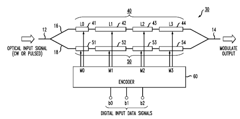
FIG. 7 illustrates an exemplary silicon-based optical modulator 30 formed in
accordance with the present invention to address the nonlinearity and
attenuation problems
associated with the use of free carrier dispersion-based modulation in a multi-
segment
modulator configuration. As shown, modulator 30 comprises the same MZI
architecture
as discussed above, including an input waveguide 12, output waveguide 14 and a
pair of
6
CA 02769854 2012-02-01
WO 2011/022308
PCT/US2010/045555
waveguiding arms 16, 18. A CW optical signal is coupled into input waveguide
12 and a
"modulated" optical signal appears along output waveguide 14, the modulation
introduced
by an electrical input (data) signal applied as an input to modulating devices
disposed
along waveguide arms 16, 18. Each waveguide arm 16, 18 is shown as comprising
multiple segments, with the electrical (data) input signals used to control
the degree of
phase modulation introduced into the propagating optical signal.
In particular, optical waveguide arm 16 is shown as comprising a first
plurality of
segments 40, in this case a set of four segments 41, 42, 43 and 44 of various
lengths
(shown as LO, Li, L2 and L3 in F1G. 7), although more than four segments can
be used.
The segment lengths are prescribed, in particular, on design criteria
described
hereinbelow, including compensating for nonlinear phase modulation and free-
carrier
induced attenuation. Optical waveguide arm 18 is shown as formed as a second
plurality
of segments 50 (including, again, four segments 51, 52, 53 and 54 of
prescribed lengths).
Each segment may be formed similar to the configuration of modulator 1 as
shown in
FIGs. 1-3; alternatively, a P-N junction silicon-based modulator as also known
in the art
may be utilized in the modulator of the present invention.
In accordance with the present invention, an input signal encoder 60 is used
to
convert a set of N input electrical data signal bits into a set of M
electrical drive signals
used to the control first and second pluralities of segments 40 and 50. As
noted above, the
number of segments M is related to the number of bits N by the relation M
2N12. For the
exemplary embodiment of FIG. 7, N=3 and M=4. Input signal encoder 40 functions
to
map the eight possible input conditions from the three-bit input electrical
data signal (b0,
bl, b2) into control signals (MO, Ml, M2, M3) for segments 20, 30. It is
advantageous
that the outputs are also digital signals, allowing for CMOS-based circuit
elements to be
used in the fabrication of the modulator. Table I, shown below, illustrates
one exemplary
encoding scheme that may be used to create control signals MO-M3:
b2 b 1 b0 MO M1 M2 M3
0 0 0 off off off off
0 0 1 on off off off
0 1 0 on on off off
0 1 1 on on on off
1 0 0 off off off on
7
CA 02769854 2012-02-01
WO 2011/022308 PCT/US2010/045555
1 0 1 off off on on
1 1 0 off on on on
1 1 1 on on on on
TABLE I
In this case, input signal encoder 60 maps the eight possible input conditions
of the
three-bit electrical data input signal into eight of the possible sixteen
output states for
control signals M0-M3. The judicious choice of the "best" eight states allows
for the
silicon-based modulator to overcome the nonlinear phase response and
attenuation
problems associated with free carrier dispersion-based modulation. It is to be
understood
that although not explicitly shown in this table or in the associated
drawings, each one of
the M control signals applied to the modulator segments actually comprises a
pair of
oppositely-biased signals. Moreover, it is to be understood that an
additional, constant
phase bias is applied to modulator 30 so as to allow it to function at the
desired operating
point.
FIG. 8 illustrates an embodiment of the present invention as configured for a
QAM
optical modulator 100. In this case, waveguide 16 is shown as associated with
the in-
phase (I) component of the QAM modulation scheme, and waveguide 18 is
associated
with the quadrature (Q) component of this scheme. A first multi-segment
modulator 110
and associated first input signal encoder 120 are disposed along waveguide 16,
as shown.
A second multi-segment modulator 130 and associated second input signal
encoder 140
are similarly disposed along waveguide 18. In order to re-combine the signals
along arms
16 and 18, a 7E/2 phase shift element 135 is disposed at the output of
modulator 130 so as
to allow for the orthogonal components to be re-aligned.
As shown, the in-phase data bit inputs IO, Ii and 12 are used as inputs to
first input
signal encoder 120, where in this particular embodiment, first input signal
encoder 120 is
shown as generating a set of six control signals MO-M5 (more particularly six
pair of
complementary control signals). This set of six control signals MO-M5 is then
used to
control a six-segment modulator structure, shown as segments 150 along a first
waveguide
16-1 and segments 152 along a second waveguide 16-2. In a similar fashion, a
set of
quadrature data bit inputs QO, QI and Q2 are used as inputs to second input
signal encoder
140, again creating a set of six control signals for segments 154 and 156
disposed along
waveguides 18-1 and 18-2, respectively. Again, encoders 120 and 140 are used
to map the
8
CA 02769854 2012-02-01
WO 2011/022308
PCT/US2010/045555
input signal bits into the "best" set of output signals that over the
nonlinearity and
attenuation problems associated with silicon-based optical modulators.
FIG. 9 is a diagram of the prior art constellation diagram associated with QAM-
64,
using a three segment modulator to directly apply the three-bit input signal
(b0, bl and b2)
to the I and Q modulators in an arrangement similar to FIG. 8 (in this case,
using only
three segments along each modulator). It is to be understood that an "ideal"
modulator
structure would yield a constellation diagram comprising an array of equally-
spaced
points. However, the various nonlinear properties of the MZI (i.e., its
inherent nonlinear
transfer function, as well as the presence of attenuation along the signal
path and the
nonlinear phase modulation) all contribute to introducing displacements in
various ones of
the 64 possible data signals with respect to their hypothetical locations.
This displacement
is particularly problematic for the "outer signals", as indicated in FIG. 9.
In accordance with the present invention, by increasing the number of segments
utilized in the modulator, and judiciously selecting the control signal input
pattern
supplied by the encoder, the attenuation associated with these signals can be
reduced.
FIG. 10(a) is a constellation diagram for an embodiment of the present
invention utilizing
a four segment modulator structure, and FIG. 10(b) is a constellation diagram
for an
embodiment utilizing a six-segment modulator. The improvement over the three-
segment
arrangement of the prior art is visible. Indeed, by increasing the number of
segments, the
error rate in the data recovered from modulated output signal at an associated
optical
receiver is significantly reduced.
FIG. 11 illustrates an alternative embodiment of the present invention, in
this case
implementing QAM-64 with a single modulator 200. In order to provide a
complete
representation of all 64 possible data bits, a set of phase modulation
segments 210 are
located "outside" of modulator 200 along output signal path 14. As shown, the
three in-
phase data bits (I0, 11 and 12), as well as the three quadrature data bits
(QO, Q1 and Q2)
are applied as inputs to a single encoder 220. The particular embodiment of
FIG. 11
comprises a six-segment modulator structure 230, with control signals M0-M5
(and their
complements) applied as drive signal inputs to separate segments 231, 232,
233, 234, 235
and 236, respectively, forming modulator structure 230. Encoder 220 thus
utilizes the I, Q
input signals to create not only the drive signals for the modulator segments
230, but also
digital drive signals 4?0, (I? I and 4?2 for phase modulation segments 210,
where the lengths
9
CA 02769854 2012-02-01
WO 2011/022308
PCT/US2010/045555
of segments 230 and drive signal patterns are also selected to address
attenuation problems
associated with the silicon-based optical modulating device.
Although not particularly illustrated, it is to be understood that the
embodiment of
the present invention as discussed above in association with FIG. 8 may be
modified to
further include a plurality of phase modulating segments disposed "outside" of
modulator
100, along output waveguide 14.
For some design applications, it may be necessary to optimize the length of
each
segment on an individual basis. Specific silicon-based limitations (such as
free-carrier
dispersion-based attenuation) are known to be a function of the length of the
MZI structure
(see, for example, the diagrams of FIGs. 6(a) and (b), which illustration
phase modulation
and attenuation as a function of the length (mm) of a silicon-based modulating
device.
However, it may also be advantageous to choose the lengths based on a
geometric series.
For example, in a five segment embodiment, the lengths may be geometrically
related by
L/2, L/4, L/8, L/16 and L/32, where L is chosen based on some criteria such as
maximum
optical modulation amplitude (OMA), extinction ratio, or the like. The
specific selected
criteria is considered to be a design consideration of the specific
implementation and not a
requirement of the present invention. FIG. 12 illustrates an alternative
arrangement 300
of the embodiment of FIG. 11 utilizing such a scheme for defining the lengths
of each
modulation segment (both segments 310 "inside" MZI 300 and segments 320
"outside" of
MZI 300). in this approach, the modulator segments may be driven in a manner
resulting
in an effective total length of 31L/32 in L/32 increments. As with the other
arrangements
discussed above, a suitably programmed encoder 330 is used to provide a
plurality of
digital drive signals to the separate segments, shown as a first set of
digital drive signals
MO ¨ M4 (of complementary form) to segments 310 within MZI and a second set of
digital drive signals O0 - (single-sided) to phase segments 320 disposed
along output
waveguide 14.
It is to be understood that the encoding technique used in the modulator of
the
present invention is applicable for a variety of different modulation schemes.
Exemplary
modulation formats include, but are not limited to, pulse amplitude modulation
(PAM-n),
which is sometimes referred to in the art as amplitude-shift-keying (ASK), QAM-
n
(implementing rectangular as well as star constellation diagrams), orthogonal
frequency
division multiplexing (OFDM), and the like. Indeed, while the present
invention has been
described with reference to several embodiments thereof, those skilled in the
art will
CA 02769854 2014-10-03
recognize various changes may be made. Therefore, the scope of the claims
should not be
limited by the preferred embodiments set forth in the examples, but should be
given the
broadest interpretation consistent with the description as a whole.
Accordingly, the invention
is not limited to what is shown in the drawings and described in the
specification, but only as
indicated in the claims appended hereto.
11