Note: Descriptions are shown in the official language in which they were submitted.
CA 02770057 2012-02-02
WO 2011/021468
PCT/JP2010/062284
-1-
DESCRIPTION
TITLE OF THE INVENTION
MULTI-BEAM LASER POWER CONTROL CIRCUIT AND
IMAGE FORMING APPARATUS USING THE SAME
TECHNICAL FIELD
The present invention relates to a multi-
beam laser power control circuit used in an image
forming apparatus, and more particularly to a multi-
beam laser power control circuit detecting the output
power of plural semiconductor lasers using a
photodiode and controlling the output power as
desired.
BACKGROUND ART
Semiconductor lasers have been widely used
in printers, optical disks, optical communications
and the like because of their compact size, lower
cost, and easiness of obtaining a laser light simply
by passing a current. However, the current-output
power (optical amount) characteristic of the
semiconductor lasers varies depending on the
environmental temperature. Because of this feature,
it is required to perform a special output power
CA 02770057 2012-02-02
WO 2011/021468 PCT/JP2010/062284
-2-
control to obtain a fixed (constant) optical output
power. The power (optical output power) control is
called Automatic Power Control (APC).
In the Automatic Power Control (APC), before
a semiconductor laser is practically used, the
semiconductor laser is operated so that the output
power of the semiconductor laser is received by using
a photodiode (FD). Then, a current value when the
output of the photodiode (FD) reaches a predetermined
level is stored in a storage means. By using the
current value, the output power is controlled to
obtain a stable output power. With the recent
increase of writing speed in printers and the like, a
method has become popular in which plural
semiconductor lasers disposed in an array shape are
simultaneously driven. In such a semiconductor laser
array, the photodiode(s) to be used for the Automatic
Power Control (APC) is integrated without fail.
However, the number of the photodiodes may be smaller
than that of the semiconductor lasers; and in some
cases, only one photodiode is integrated.
When the number of the photodiode (FD) is
only one, it is required to separately drive the
semiconductors one by one. FIG. 7 is a block diagram
showing a prior-art relationship among a multi-beam
CA 02770057 2012-02-02
WO 2011/021468 PCT/JP2010/062284
-3-
laser power control circuit 15, a semiconductor laser
array (multi-beam unit) 5, and an image control
circuit 54. As shown in FIG. 7, the semiconductor
laser array (multi-beam unit) 5 includes two
semiconductor lasers (LD1, LD2) and only one
photodiode 3 corresponding to each of the
semiconductor lasers (LD1, LD2).
In the semiconductor laser array (multi-beam
unit) 5 of FIG. 7, if the Automatic Power Control
(APC) is simultaneously performed on those two
semiconductor lasers (LD1, LD2), the photodiode 3
regards the total output power from the two
semiconductor lasers (LD1, LD2) as the basic output
power of each of the two semiconductor lasers (LD1,
LD2). Namely, in this case, the APC may be
terminated before the power output from the two
semiconductor lasers (LD1, LD2) becomes sufficient.
To address such an inconvenience,
conventionally, for example, there is a known timing
chart in which a time margin is inserted between
plural timings at which corresponding APC execution
signals (APC1, APC2) are input into the multi-beam
laser power control circuit 15, the time margin being
determined so as to prevent the APC execution signals
(APC1, APC2) from being overlapped with each other
CA 02770057 2014-04-10
76311-9
-4-
when the APC execution signals (APC1, APC2) are input
into the multi-beam laser power control circuit 15 in
view of parasitic resistance/capacitance due to
substrate wirings and the like, the APC execution
signals (APC1, APC2) corresponding to two
semiconductor lasers and being output from the image
control circuit 54 that is provided in a preceding
-stage of the multi-beam laser power control circuit
and that controls the multi-beam laser power
10 control circuit 15 (see, for example, a timing chart
of FIG. 8 of Patent Document 1, a timing chart =of FIG.
9 of Patent Document 2, and a timing chart of FIG. 8
of Patent Document 3).
. 15= SUMMARY OF THE INVENTION
As shown in FIG. 7, generally, the multi-
beam laser power control circuit 15 and the image
control circuit 54 provided in the preceding stage of
the multi-beam laser power control circuit 15 are
disposed in different substrates. In this
configuration, in order to reduce the influence of
external noises, a LPF (Low Pass Filter) circuit 52
or the like may be inserted in a preceding stage of
the multi-beam laser power control circuit 15 to
CA 02770057 2012-02-02
WO 2011/021468
PCT/JP2010/062284
-5-
avoid the malfunction of the Automatic Power Control
(APC) due to surrounding external noises. Namely, in
a case where the Automatic Power Control (APC) is
sequentially performed on plural channels, an extra
delay component due to the LPF (Low Pass Filter)
circuit 52 may be added to the APC execution signals.
Further, the delay component may vary depending on
the LPF (Low Pass Filter) circuit 52. Therefore, it
is required to determine the time margin between the
APC execution signals (channels) in view of the
variance of the delay component.
On the other hand, the time period in which
the Automatic Power Control (APC) can be performed is
limited. For example, as shown in FIG. 8, in a laser
printer capable of performing high-speed printing or
the like, a scanning time for writing one line may be
equal to or less than 200 ps, and only approximately
5 ps may be allowed to be used for performing the
Automatic Power Control (APC).
The longer the time period to perform the
Automatic Power Control (APC) becomes, the more
accurately the output power of the semiconductor
laser can be controlled. From this point of view,
the longer the time period to perform the Automatic
Power Control (APC) becomes, the better. Typically,
CA 02770057 2014-04-10
76311-9 =
-6-
the time period if equal to or more than 2 ps. Under
the condition that the Automatic Power Control (APC)
for plural channels is required to be performed
within the limited time period allowed for the
Automatic Power Control (APC), the time margin
between the APC execution signals (channels) to be
properly set becomes a practical loss in the time
period of the Automatic Power Control (APC) and is a
disadvantageous factor in adjusting the output power
of the semiconductor lasers.
The present invention is made in light of
the above circumstances, and may provide a multi-beam
laser power control circuit capable of controlling to
perform accurate Automatic Power Control (APC) =for a
long period as long as possible even when the number
of semiconductor lasers is increased without
necessarily performing the Automatic Power Control
(APC) of the image control circuit in view of the
influences of the substrate configuration and the low
pass filter (Noise reduction circuit), and an image
forming apparatus using the multi-beam laser power
control circuit.
According to one aspect of the present
CA 02770057 2012-02-02
WO 2011/021468
PCT/JP2010/062284
-7-
invention, a multi-beam laser power control circuit
includes a light receiving element receiving power
output from semiconductor lasers to control output
power of a semiconductor laser array having plural
semiconductor lasers, automatic power control
circuits (APC circuits) receiving corresponding
automatic power control execution signals (APC
execution signals) and controlling emission power
output from semiconductor lasers based on the
received corresponding automatic power control
execution signals (APC execution signals) so that the
emission power output from the respective
semiconductor lasers are set to predetermined
emission power based on output from the light
receiving element, and APC execution signal input
terminals inputting the corresponding automatic power
control execution signals, a number of the input
automatic power control execution signals
corresponding to a number of the automatic power
control circuits (APC circuits). Further, in the
multi-beam laser power control circuit, when plural
APC execution signals input to the corresponding APC
execution signal input terminals are overlapped in
time domain, the automatic power control circuits
(APC circuits) to be preferentially operated is
CD, 02770057 2014-04-10
76311-9
-8-
determined based on input timings of the plural APC
execution signals and *operated.
Further, in the multi-beam laser power
control circuit according to an aspect of the present
invention, at the input timings of the APC execution
signals, the automatic= power control circuit (APC
circuit) corresponding to the APC execution signal
that is input earlier may be preferentially operated;
otherwise, at the input timings of the APC execution
signals, the automatic power control circuit (APC
circuit) corresponding to the APC execution signal
that is input later may be preferentially operated.
= Further, the multi-beam laser power control
circuit according to an aspect of the present
invention may include a reporting unit externally
reporting information indicating that, when the
received plural APC execution signals are overlapped
in time domain, the received plural APC execution
= signals are overlapped.
Further, in the multi-beam laser power
control circuit according to an aspect of the present
invention, when plural APC execution signals are
simultaneously received, the automatic power control
circuits (APC circuits) may be preferentially
=operated based on a predetermined priority order.
CA 02770057 2014-04-10
76311-9
- 8a -
According to another aspect of the present invention,
there is provided a multi-beam laser power control circuit
comprising: a light receiving element configured to receive
power output from semiconductor lasers to control output power
of a semiconductor laser array having plural semiconductor
lasers; automatic power control circuits (APC circuits)
configured to receive corresponding automatic power control
execution signals (APC execution signals) and control emission
power output from semiconductor lasers based on the received
corresponding automatic power control execution signals (APC
execution signals) so that the emission power output from the
respective semiconductor lasers are set to predetermined
emission power based on output from the light receiving
element; -and APC execution signal input terminals configured to
input the corresponding automatic power control execution
signals, a number of the input automatic power control
execution signals corresponding to a number of the automatic
power control circuits (APC circuits), wherein when plural APC
execution signals input to the corresponding APC execution
signal input terminals are overlapped in time domain, the
automatic power control circuits (APC circuits) to be
preferentially operated is determined based on input timings of
the plural APC execution signals and operated; the multi-beam
laser power control circuit further comprising a reporting unit
configured to externally report information indicating that,
when the received plural APC execution signals are overlapped
in time domain, the received plural APC execution signals are
overlapped.
= CA 02770057 2014-04-10
76311-9
= -9-
= According to an aspect of the present
invention, there is provided an image forming
apparatus including any one of the above-described
multi-beam laser power control circuits.
5=
According to an embodiment of the present
invention, it may become possible to transmit the APC
execution signals to the multi-beam laser power
control circuit without necessarily performing a
complicated timing control including, for example,
controlling the delay due to surrounding external
noises in the image control circuit disposed in the
preceding stage of the multi-beam laser power control
circuit. For example, even when two or more APC
execution signals each indicating APC execution
status are transmitted from the image control circuit
disposed in the preceding stage, it may becbme
possible for the multi-beam laser power control
circuit to perform the Automatic Power Control (APC)
by determining the priority order of the APC
execution signals without causing overlaps among the
APC execution signals. Further, when plural
Automatic Power Controls (APC) are performed within a
short time period, the plural Automatic Power
CA 02770057 2012-02-02
WO 2011/021468
PCT/JP2010/062284
-10-
Controls (APC) may be performed sequentially without
necessarily setting the time margin between the APC
execution signals (channels). Because of this
feature, it may become possible to perform more
accurate Automatic Power Control (APC).
Further, it may become possible to reduce
the time period required for performing the Automatic
Power Control (APC), thereby enabling realizing a
high-speed image forming apparatus.
Patent Document 1: Japanese Patent Application
Publication No. 2006-035703
Patent Document 2: Japanese Patent Application
Publication No. 2005-153283
Patent Document 3: Japanese Patent Application
Publication No. 2001-257418
BRIEF DESCRIPTION OF THE DRAWINGS
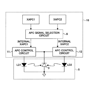
FIG. 1 is a schematic block diagram showing
a multi-beam laser power control circuit according to
a first embodiment of the present invention;
FIG. 2 is an exemplary timing chart
corresponding to an example based on a selection
logic employed in an APC signal selection circuit
according to the first embodiment of the present
invention;
CA 02770057 2012-02-02
WO 2011/021468 PCT/JP2010/062284
-11-
FIG. 3 is an exemplary timing chart
corresponding to an example based on another
selection logic employed in the APC signal selection
circuit according to the first embodiment of the
present invention;
FIG. 4 is an example of a circuit diagram of
the APC signal selection circuit according to the
first embodiment of the present invention;
FIG. 5 is an exemplary timing chart
including a signal for externally reporting
information indicating that the APC execution signals
are overlapped with each other;
FIG. 6 is another example of a circuit
diagram of the APC signal selection circuit according
to the first embodiment of the present invention;
FIG. 7 is a block diagram showing a prior-
art relationship among the multi-beam laser power
control circuit, a semiconductor laser array (a
multi-beam unit), and an image control circuit; and
FIG. 8 is a schematic drawing showing a
relationship among a one-line scanning period, an APC
execution allowed period, an effective writing period,
and a loss period in view of a delay to the multi-
beam laser power control circuit.
CA 02770057 2012-02-02
WO 2011/021468
PCT/JP2010/062284
-12--
DESCRIPTION OF THE REFERENCE NUMERALS
LD1, LD2: SEMICONDUCTOR LASER
3: PHOTODIODE
5: SEMICONDUCTOR LASER ARRAY (MULTI-BEAM UNIT)
6: APC SIGNAL SELECTION CIRCUIT
10,11,12: APC CONTROL CIRCUIT
15,16: MULTI-BEAM LASER POWER CONTROL CIRCUIT
24: RS LATCH CIRCUIT
26: DELAY CIRCUIT
54: IMAGE CONTROL CIRCUIT
MODE FOR CARRYING OUT THE INVENTION
In the following, preferred embodiments of
the present invention are described with reference to
the accompanying drawings.
First embodiment
FIG. 1 is a schematic block diagram of a
multi-beam laser power control circuit 16 according
to a first embodiment of the present invention. In
FIG. 1, in addition to the block diagram of the
multi-beam laser power control circuit 16, a block
diagram of a semiconductor laser array (multi-beam
unit) 5 is included.
As shown in FIG. 1, the semiconductor laser
CA 02770057 2012-02-02
WO 2011/021468 PCT/JP2010/062284
-13-
array (multi-beam unit) 5 includes two semiconductor
lasers (LD1, LD2) and one photodiode 3 corresponding
to those two semiconductor lasers (LD1, LD2).
Further, the multi-beam laser power control circuit
16 of FIG. 1 includes an APC signal selection circuit
6, an APC control circuit 11 for LD1, and an APC
control circuit 12 for LD2, and APC execution signal
input terminals to externally input the APC execution
signals. The APC execution signals are input to the
respective APC execution signal input terminals, the
number of the APC execution signals corresponding to
that of the APC control circuits 11 and 12.
Further, in FIG 1, the symbols "XAPC1" and
"XAPC2" refer to the APC execution signals from an
external circuit (such as an image control circuit)
("external APC execution signal(s)"). As described
above, in this description, it is assumed that when
the APC execution signal is "Low", the APC is to be
executed ("APC execution logic"). The APC signal
selection circuit 6 receives the "XAPC1" and "XAPC2".
Then, in a period when the both received "XAPC1" and
"XAPC2" are "Low" (i.e., in the APC execution logic ),
at the timing when both of the "XAPC1" and "XAPC2"
are input (i.e., become "low") (input timing of both
of the "XAPC1" and "XAPC2"), the APC signal selection
ak 02770057 2014-04-10
76311-9 ,
=
. -14-
circuit 6 selects one of the received signals in a
manner such that the APC signal selection circuit 6
sets the selected one to be "Low" and the other to be
"High" and outputs the results as "Internal-XAPC 1"
and "Interna1-XAPC2". The symbols "Internal-XAPC 1"
and "Internal-XAPC2" refer to the APC execution
signals finely adjusted by the APC signal selection
=
circuit 6 based on the "XAPC1" and "XAPC2",
respectively and transmitted within the multi-beam
laser power control circuit 16 ("internal APC
execution signal(s)"): The "Internal-XAPC 1" is
input into the APC control circuit 11 to control the
APC execution of the semiconductor laser LD1.
Similarly, the "Internal-XAPC 2" is input into the
APC control circuit 12 so as to control the APC
execution of the semiconductor laser LD2.
As described above, in a period when bothof
the "XAPC1" and "XAPC2" are "Low", the APC signal
selection circuit 6 selects one of the "XAPC1" and
"XAPC2" signals, sets the selected signal to "Low",
sets the other signal to "High", and outputs the
signals as the "Internal-XAPC 1" and the '"Internal-
XAPC2". IN this case, for example, at the input
timing of both of the APC execution signals (the
"XAPC1" and "XAPC2"), the APC signal selection
=
CA 02770057 2012-02-02
WO 2011/021468
PCT/JP2010/062284
-15-
circuit 6 may employ a selection logic that a higher
priority is given to the operation of the APC control
circuit corresponding to the APC execution signal
that is input earlier (i.e., the APC signal selection
circuit 6 sets only the internal APC execution signal
to "Low", the internal APC execution signal
corresponding to the external APC execution signal
that is input earlier). FIG. 2 is an example of
timing chart corresponding to this selection logic.
FIG. 2 is an exemplary timing chart of a
multi-beam laser power control circuit dedicated to a
two-channel LD-A. In this timing chart, a symbol
"RST" refers to a reset signal of the multi-beam
laser power control circuit 16, and the reset status
is released when the reset signal is "Low". The
symbols "XAPC1" and "XAPC2" refer to the external APC
execution signals, and the APC is to be executed (APC
execution logic) when the corresponding external APC
execution signal is "Low". Namely, the status that
the "XAPC1" and "XAPC2" are "Low" indicates that each
execution of the APC of the respective LD1 and LD2 is
externally instructed. The symbols "Internal-XAPC1"
and "Internal-XAPC2" refers to the internal APC
execution signals. The status that the internal APC
execution signal is "Low" indicates that the
CA 02770057 2014-04-10
76311-9
-16-
corresponding APC is executed (APC execution logic).
Namely, when the "Internal-XAPC1" and "Internal-
XAPC2" are "Low", the APC of the respective LD1 and
LD2 is actually executed.
Referring back to FIG. 2, after the RST is
released, in the period of (1), the "XAPC1" and the
"XAPC2" have their own "Low" periods; and accordingly,
the APC for the corresponding semiconductor lasers
(LD1, LD2) is separately executed.
. .Next, in the period of (2), there is a
period when both of "XAPC1" and "XAPC2" are "Low".
However, before this period, the "XAPC1" becomes
"Low" earlier than the "XAPC2". Therefore, in this
period, even when the "XAPC2" becomes "Low", the
"Internal-XAPC2" remains "High". After that, the
"Interna1-XAPC2" becomes effective ("Low") only when
"XAPC2" remains "Low" and the "XAPC1" is "High".
In the period of (3), in contrast to the
period of period (2), while the "XAPC2" remains "Low",
the "XAPC1" becomes "Low". In this case also,
"Internal-XAPC1" does not become effective ("Low") until
= "XAPC2" becomes "High".
As described above, FIG. 2 shows an example
of a timing chart showing a case where, at the .input
timings of the external APC execution signals, the
CA 02770057 2012-02-02
WO 2011/021468
PCT/JP2010/062284
-17-
APC signal selection circuit 6 employs the selection
logic that a higher priority is given to the
operation of the APC control circuit corresponding to
the external APC execution signal that is input
earlier. However, in contrast, the signal selection
circuit 6 may employ another selection logic that a
higher priority is given to the operation of the APC
control circuit corresponding to the external APC
execution signal that is input later. FIG. 3 shows
an example of the timing chart corresponding to the
selection logic.
Next, FIG. 4 shows an exemplary APC signal
selection circuit 6 based on the selection logic that
"a higher priority is given to the operation of the
APC control circuit corresponding to the external APC
execution signal that is input earlier", the
selection logic being illustrated in the timing chart
of FIG. 2. In the APC signal selection circuit 6,
the logic sum (OR) between the "XAPC1" or the "XAPC2"
and the "RST" is given as the "XAPCla" or the
"XAPC2a", respectively. A NOR-type RS latch circuit
24 selects only one of the "XAPCla" and the "XAPC2a"
which is input earlier as effective. Based on a
result of this selection, the NOR-type RS latch
circuit 24 outputs the "Internal-XAPC1" and the
CA 02770057 2012-02-02
WO 2011/021468 PCT/JP2010/062284
-18-
"Internal-XAPC2". As described above, the "Internal-
XAPC1" and the "Internal-XAPC2" are the APC execution
signals within the multi-beam laser power control
circuit 16 (internal APC execution signals).
In the prior art, the "XAPC1" and "XAPC2"
are directly used as the "Internal-XAPC1" and
"Internal-XAPC2". However, by adding the small-scale
circuit according to an embodiment of the present
invention as shown in FIG. 4, it may become possible
to avoid the occurrence of a power control error due
to simultaneous APC execution between plural channels.
Further, as shown in FIG. 4, the APC signal
selection circuit 6 may include a delay circuit 26
that delays the corresponding APC execution signal
when, for example, the APC execution signals are
simultaneously input in plural channels. By having
the delay circuit 26 in FIG. 4, the "XAPC2a" signal
within the APC signal selection circuit 6 is delayed,
so that a higher priority is given to the "XAPCla"
signal and as a result, only the "Internal-XAPC1"
becomes low. Namely, a higher priority is given to
the APC execution of the LD1.
As described above, by inserting the delay
circuit 26 as described= in FIG. 4, it may become
possible to determine which semiconductor laser has a
CA 02770057 2012-02-02
WO 2011/021468 PCT/JP2010/062284
-19-
higher priority to execute the APC when plural APC
execution signals are simultaneously input.
Embodiment generating a signal indicating an overlap
of APC execution signals
First, FIG. 5 is a timing chart including a
timing of a signal externally reporting an overlap of
the APC execution signals when the APC execution
signals of plural channels are overlapped in time
domain (external report signal).
In the timing chart of FIG. 5, the "XERR"
signal corresponds to the external report signal.
The "Low" status of the "XERR" signal indicates that
the APC execution signals are overlapped. In this
case, if the "XERR" signal reports only the period
during the APC execution signals are exactly
overlapped, since the period during the APC execution
signals are overlapped is a very short period such as
several ns (nanoseconds), the period may not be
correctly detected by an external receiving device
(e.g., control circuit). To overcome this
inconvenience, as shown in the timing chart of FIG. 5,
the APC signal selection circuit 6 adds several ps
(microseconds) (one ps in FIG. 5) to the period
during the APC execution signals are overlapped to
elongate the report signal.
CA 02770057 2012-02-02
WO 2011/021468 PCT/JP2010/062284
-20-
FIG. 6 shows an exemplary APC signal
selection circuit 6 generating the elongated report
signal. The circuit of FIG. 6 is basically similar
to that of FIG. 4 except that the circuit of FIG. 6
includes an OR circuit 28 and a Delay section, the OR
circuit 28 receiving the "XAPCla" and the "XAPC2a"
signals.
The Delay section includes an inverter
circuit 34 having an input connected to a resistor 30
and a capacitor 32. As soon as both the "XAPCla" and
the "XAPC2a" are "Low", the "XERR" signal is "Low".
However, even when at least one of the "XAPCla" and
the "XAPC2a" is returned to "High", due to a time
constant formed by the resistance of the resistor 30
and the capacitance of the capacitor 32, a delay is
generated between a period from "Low" to "High" of
the "XERR" signal. By doing in this way, the period
of the report signal may be elongated.
Other embodiment
In the above description, a configuration of
the multi-beam laser power control circuit dedicated
to a two-channel LD-A is described. However, the
present invention may also be applied to a multi-beam
laser power control circuit for an LD-A having three
CA 02770057 2014-04-10
76311-9
- 21 -
or more channels, and the present invention may be realized in
a circuit for three or more channels in a similar manner to
that for the two-channel LD-A as described above.
Further, by using the above-described multi-beam
laser power control circuit in an image forming apparatus, it
may become possible to realize a high-speed image forming
apparatus capable of reducing the exact time period allowed for
the APC execution.