Note: Descriptions are shown in the official language in which they were submitted.
CA 02770386 2012-02-07
WO 2011/016817 PCT/US2009/066149
ASSEMBLY AND METHOD FOR ILLUMINATING
THROUGH A CIRCUIT BOARD
Reference to Related Application
[0001] The present application claims the benefit of U.S. Provisional Patent
Application
No. 61/232,263, filed August 7, 2009, whose disclosure is hereby incorporated
by reference
in its entirety into the present disclosure.
Field of the Invention
[0002] The present invention relates to illuminating through a circuit board.
In particular,
the present invention relates to an assembly and a method for illuminating
through a circuit
board so that the light from the light source substantially maintains its
color and intensity.
Background of the Invention
[0003] Known circuit boards are made from dielectric materials that are
opaque. For
example, many circuit boards are made from dielectric materials, such as Flame
Retardant 4
or FR4, which is formed from woven glass and epoxy, or some other epoxy-based
material.
Such dielectric materials are usually green or yellow, and the green or yellow
coloring is
inconsistent. Thus, when these dielectric materials are backlit or illuminated
such that light
has to travel through the dielectric material, the light traveling through the
dielectric material
changes color or loses its intensity. That is, the dielectric material filters
the light that travels
through it. Therefore, the light source that provides the light that travels
through the
dielectric material must emit a light with a color that compensates for the
filtering or emit a
light with a stronger intensity. However, a light source that emits a light
with stronger
intensity consumes more power and produces more heat.
CA 02770386 2012-02-07
WO 2011/016817 PCT/US2009/066149
[0004] Thus, a dielectric material that compensates for the filtering of light
is needed.
However, known dielectric material that compensate for the filtering of light,
such as
polyester flex circuits, are not compatible with lead free solders or two-
sided traces. Also,
polyester flex circuits cannot withstand the heat required for lead free
solders. Lead-free
solder is needed for certain circuit elements or components, for example,
those associated
with capacitive or field effect circuits and sensors. Thus, known dielectric
material cannot be
used with such circuit elements or components.
[0005] Also, known dielectric materials do not adhere well to another surface.
In some
applications, printed circuit boards are mated to another surface for mounting
or mechanical
support. If the other surface has an irregular shape or a non-planar contour,
the known
printed circuit board does not have the flexibility to conform to the
irregular shape or the non-
planar contour. Furthermore, pressure sensitive tape and adhesives are used to
mate the
printed circuit board to another surface. However, pressure sensitive tape and
adhesives are
prone to forming air gaps between the printed circuit board and the other
surface, thereby
forming thick, unreliable, and non-uniform bonding between printed circuit
boards and their
mating surfaces. Also, for devices using capacitive or field effect circuits
and sensors, air
gaps impair their performance. Furthermore, pressure sensitive tape and
adhesives change
the color or intensity of light passing through them.
[0006] Thus, there is a need for a dielectric material that can be backlit
such that the light
traveling through the dielectric material does not substantially change color
or lose its
intensity. If the dielectric material is mated to another surface, the mating
should be thin,
reliable, uniform, and allow light to pass without substantially changing its
color or intensity.
2
CA 02770386 2012-02-07
WO 2011/016817 PCT/US2009/066149
Also, the same dielectric material should be compatible with lead free solder
and two-sided
traces. Furthermore, the dielectric material should be flexible so that it can
conform to the
contours of another surface.
Summary of the Invention
[0007] Accordingly, an aspect of the invention may provide an assembly that
includes a
substrate, a flexible layer, and an adhesive mating the substrate and the
flexible layer. The
substrate has a first surface and a second surface opposite the first surface.
The flexible layer
has a first surface and a second surface opposite the first surface. The
flexible layer has a
thickness such that light passes through the flexible layer without
substantial change to a
color or an intensity of the light and such that the flexible layer
substantially conforms to a
shape of the substrate. The adhesive mates the second surface of the substrate
and the first
surface of the flexible layer and has a viscosity that substantially fills in
a texture of at least
one of the second surface of the substrate and the first surface of the
flexible layer. The
adhesive also forms substantially no air gaps.
[0008] Another aspect of the invention may provide an assembly that includes a
substrate, a flexible layer, and an adhesive mating the substrate and the
flexible layer. The
substrate has a first surface and a second surface opposite the first surface
and allows some
portion of light to pass through the first surface and the second surface. The
flexible layer
has a first surface and a second surface opposite the first surface and allows
some portion of
light to pass through the first surface and the second surface. The flexible
layer has a
thickness such that light passes through the flexible layer without
substantial change to a
3
CA 02770386 2012-02-07
WO 2011/016817 PCT/US2009/066149
color or an intensity of the light and such that the flexible layer
substantially conforms to a
shape of the substrate. The adhesive mates the second surface of the substrate
and the first
surface of the flexible layer. The adhesive allows some portion of light to
pass through the
adhesive and has a viscosity that substantially fills in a texture of at least
one of the second
surface of the substrate and the first surface of the flexible layer. The
adhesive also forms
substantially no air gaps.
[0009] Yet another aspect of the invention may provide a method of
manufacturing an
assembly. The method includes the steps of. providing a substrate with a first
surface and a
second surface opposite the first surface; providing a flexible layer with a
first surface and a
second surface opposite the first surface; placing an adhesive on at least one
of the second
surface of the substrate and the first surface of the flexible layer; filling
in a texture of at least
one of the second surface of the substrate and the first surface of the
flexible layer with the
adhesive; and pressing together the substrate, the adhesive, and the flexible
layer. The
substrate allows some portion of light to pass through the first surface and
the second surface.
The flexible layer allows some portion of light to pass through the first
surface and the
second surface.
[0010] Other objects, advantages and salient features of the invention will
become
apparent from the following detailed description, which, taken in conjunction
with the
annexed drawings, discloses exemplary embodiments of the present invention.
4
CA 02770386 2012-02-07
WO 2011/016817 PCT/US2009/066149
Brief Description of the Drawings
[0011] A more complete appreciation of the invention and many of the attendant
advantages thereof will be readily obtained as the same becomes better
understood by
reference to the following detailed description when considered in connection
with the
accompanying drawings, wherein:
[0012] FIG. I is a front elevational view of an assembly according to an
exemplary
embodiment of the present invention;
[0013] FIG. 2 is a cross-sectional view of the assembly illustrated in FIG. 1
along line 2-
2;
[0014] FIG. 3 is a side elevational view of an apparatus for manufacturing the
assembly
illustrated in FIG. 1;
[0015] FIG. 4 is a side elevational view of the apparatus illustrated in FIG.
3 with an
upper die set and a lower die set closed;
[0016] FIG. 5 is a perspective view showing a step in the manufacture of the
assembly
illustrated in FIG. 1;
[0017] FIG. 6 is a perspective view showing another step in the manufacture of
the
assembly illustrated in FIG. 1;
[0018] FIG. 7 is a perspective view showing another step in the manufacture of
the
assembly illustrated in FIG. 1;
[0019] FIG. 8 is a perspective view showing another step in the manufacture of
the
assembly illustrated in FIG. 1;
CA 02770386 2012-02-07
WO 2011/016817 PCT/US2009/066149
[0020] FIG. 9 is a perspective view showing another step in the manufacture of
the
assembly illustrated in FIG. 1;
[0021] FIG. 10 is a perspective view showing another step in the manufacture
of the
assembly illustrated in FIG. 1;
[0022] FIG. 11 is a perspective view showing another step in the manufacture
of the
assembly illustrated in FIG. 1;
[0023] FIG. 12 is a perspective view showing another step in the manufacture
of the
assembly illustrated in FIG. 1;
[0024] FIG. 13 is a perspective view showing another step in the manufacture
of the
assembly illustrated in FIG. 1;
[0025] FIG. 14 is a perspective view showing another step in the manufacture
of the
assembly illustrated in FIG. 1; and
[0026] FIG. 15 is a perspective view showing another step in the manufacture
of the
assembly illustrated in FIG. 1
Detailed Description of the Invention
[0027] Referring to FIGS. 1-15, the present invention provides an apparatus
and a method
for illuminating a circuit board such that the light traveling through the
circuit board does not
substantially change color or lose its intensity. Also, the apparatus and
method may be used
with lead free solder and two-sided traces.
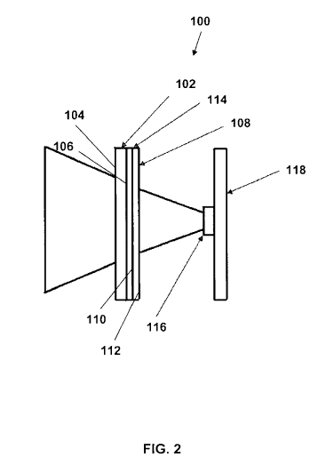
[0028] Turning to FIGS. I and 2, an assembly 100 is shown. The assembly 100
includes
a substrate 102 with a first surface 104 and a second surface 106 opposite the
first surface
6
CA 02770386 2012-02-07
WO 2011/016817 PCT/US2009/066149
104, a flexible layer 108 with a first surface 110 and a second surface 112
opposite the first
surface 110, and an adhesive 114 between the substrate 102 and the flexible
layer 108. In the
embodiment shown, the assembly 100 is illuminated by a light source 116. The
depicted
light source 116 is mounted to an illumination printed circuit board 118.
However, in other
embodiments, the light source 116 need not be mounted to an illumination
printed circuit
board 118. Also, the light source 116 can be an incandescent bulb, fluorescent
bulb, light
emitting diode, combinations of the aforementioned, or any other device that
provides light or
illumination.
[0029] For the sake of simplifying the description, the invention is described
in reference
to an embodiment where the assembly 100 provides a substrate 102 with which a
user
interacts. The user interactions on the first surface 104 of the substrate 102
actuate one or
more capacitive or field effect devices disposed on the flexible layer 108
adjacent to the
substrate 102. The first surface 104 of the substrate 102 can include indicia
such as words,
diagrams, pictures, signs, and other indicators that can be imprinted,
printed, etched, sculpted,
painted, adhered, or other mated to the first surface 104. The user touches
the first surface
104 near one or more of the capacitive or field effect devices, and the touch
on the first
surface 104 actuates the one or more capacitive or field effect devices
disposed on the
flexible layer 108. Such an assembly 100 can be used, for example, in an
automobile to
control or manipulate one or more functions of a system of the automobile. For
example, the
first surface 104 of the substrate 102 can have indicia for temperature
control and the flexible
layer 108 can have a capacitive device associated with the indicia for
temperature control.
The light source 116 can emit light through the substrate 102 and the flexible
layer 108 and
7
CA 02770386 2012-02-07
WO 2011/016817 PCT/US2009/066149
thus illuminate the indicia for temperature control on the first surface 104
of the substrate 102
and the associated capacitive device on the flexible layer 108 such that the
user can visually
perceive the indicia and the associated capacitive device. Thus, when the user
touches the
first surface 104 near the indicia for temperature control, the associated
capacitive device on
the flexible layer 108 is actuated and sends a signal that changes the
temperature setting of an
air conditioning system or heating system. However, the invention is not
limited to such an
embodiment and can be applied to any assembly 100 that requires a
substantially transparent
or translucent flexible layer 108 coupled to a substrate 102.
[0030] The substrate 102 can provide mechanical support, an interface for a
user, a
surface 104 for decorative features, combinations of the aforementioned, or
some other
similar function. Although the substrate 102 is shown as being a generally
flat board, the
substrate 102 can have an irregular shape or contour. The second surface 106
of the substrate
may be mated to the flexible layer 108. The substrate 102 can be made from
plastic,
thermoset, thermoset polyethylene, thermoplastic such as acrylic or
acrylonitrile butadiene
styrene, thermoplastic polymer such as polycarbonate, thermoplastic
fluoropolymer,
fluorocarbon-based polymer, polyethylene, polyvinyl chlorides, polyvinylidene
fluoride,
ethylene tetrafluoroethylene, silicone, glass, combinations of the
aforementioned, or any
other rigid material that is substantially transparent, translucent, or allows
some portion of
light to pass. In the embodiment shown, the substrate 102 is made from
polycarbonate and
acrylonitrile butadiene styrene (ABS).
[0031] The flexible layer 108 provides a surface 110 or 112 for mounting
components.
The flexible layer 108 is flexible so that it can substantially match the
shape and contour of
8
CA 02770386 2012-02-07
WO 2011/016817 PCT/US2009/066149
the substrate 102. The flexible layer 108 is also substantially transparent,
translucent, or
white to allow at least a portion of light to travel through it with
substantially no change in
the color or intensity of the light. In the embodiment shown, components are
mounted on the
surface 110 or 112 to form one or more circuits. The components can be surface
mount
resistors, application specific integrated circuits, capacitors, connectors,
traces, or some other
component that provides a pathway for an electrical signal or manipulates an
electrical signal.
The flexible layer 108 can be made from a polytetrafluoroethylene (PTFE) film,
plastic,
thermoset, thermoset polyethylene, thermoplastic such as acrylic or
acrylonitrile butadiene
styrene, thermoplastic polymer such as polycarbonate, thermoplastic
fluoropolymer,
fluorocarbon-based polymer, polyethylene, polyvinyl chlorides, polyvinylidene
fluoride,
ethylene tetrafluoroethylene, silicone, constructs containing glass or glass
fibers,
combinations of the aforementioned, or any other rigid material that is
substantially
transparent or translucent and flexible enough to conform to the shape and
contours of the
substrate. In the embodiment shown, the flexible layer 108 is made from thin,
flexible FR408
with substantially no ultraviolet inhibitors or doping. FR408 is made from
resin-reinforced
glass fibers and is commercially available from Isola Global. Also, a flexible
layer 108 with
a thickness of approximately 0.08 mm provides optimal characteristics for
light transmission
and flexibility for matching the contours of the substrate 102.
[0032] The adhesive 114 couples the substrate 102 and the flexible layer 108.
The
adhesive 114 can be substantially transparent, translucent, or allow some
portion of light to
pass so that, when the adhesive 114 is used to mate the substrate 102 and the
flexible layer
104, the adhesive 114 allows at least some portion of light to pass without
substantially
9
CA 02770386 2012-02-07
WO 2011/016817 PCT/US2009/066149
changing the color or intensity of the light. Furthermore, the adhesive 114
can form a thin
mating that is more reliable and more uniform than a mating formed from
pressure sensitive
tape and adhesives. The adhesive 114 can be a solvent-free plastic adhesive
(such as
acrylated urethane commercially available as Dymax 3069), a solvent-free glob
top chip
encapsulant (such as modified urethane commercially available as the Dymax
9001 series of
adhesives), modified acrylate (such as those commercially available as the
Loctite 3492
series of adhesives or the Loctite 3493 series of adhesives), modified acrylic
(such as those
commercially available as the Loctite 3494 series of adhesives), or any other
appropriate
adhesive that cures substantially transparent or translucent. The adhesive 114
can be an
ultraviolet light (UV) or natural light curable adhesive. In an embodiment
using UV light
curable adhesive, the flexible layer 108 has substantially no UV blocking
agent so that UV
light can substantially pass through the flexible layer 108 to cause curing of
the UV light
curable adhesive. In the embodiment shown, the adhesive is a UV or natural
light curable
adhesive, such as Dymax 3069, and the flexible layer 108 is made from FR408
with
substantially no UV blocking agent. In other embodiments, the adhesive 114 can
be a heat
curable adhesive such as thermoplastic or chemical reaction curable adhesive
such as
polyvinyl acetate, epoxy, polyurethane, cyanoacrylate polymers,
polychloroprene, acrylate
based polymers, a resin and its corresponding accelerant, and similar
adhesives.
[0033] Before curing, the adhesive 114 can be disposed on either the second
surface 106
of the substrate or the first surface 110 of the flexible layer 108 as a thin,
uniform coating.
Also, when the adhesive 114 is made from UV or natural light curable adhesive,
it
substantially prevents formation of air gaps between the substrate 102 and the
flexible layer
CA 02770386 2012-02-07
WO 2011/016817 PCT/US2009/066149
108. Thus, when a capacitive or field effect circuit, device, or sensor is
placed on the flexible
layer 108, air gaps do not substantially impair the performance of the
capacitive or field
effect circuit, device, or sensor.
[0034] In addition, in the embodiment where the adhesive 114 is a UV or
natural light
curable adhesive, the adhesive 114 can aid in making the substrate 102 or the
flexible layer
108 more transparent, more translucent, or allow at least some portion of
light to pass more
readily. If the adhesive 114 has a viscosity so that it allows the adhesive
114 to fill in the
texture of the surface 104, 106, 110, or 112, then the adhesive 114 can make
the substrate 102
or the flexible layer 108 more transparent, more translucent, or allow some
portion of light to
pass more readily. Such an adhesive 114 acts as a wetting agent and allows
more light to
pass through the substrate 102 or the flexible layer 108.
[0035] The flexible layer 108 may be connected to the illumination printed
circuit board
118 by an electrical pathway. In the embodiment shown, a flat flexible cable
(FFC)
connector connects the flexible layer 108 and the illumination circuit board
118. In other
embodiments, the flexible layer 108 and the illumination circuit board 118 can
be connected
by a trace, a wire, a cable, a coaxial cable, a wireless transmission path,
combinations of the
aforementioned, or any other pathway for signals between two components.
[0036] Referring to FIGS. 3-4, an apparatus 200 for manufacturing the assembly
100 is
shown. Turning to FIG. 3, the apparatus 200 includes an upper die set 202 and
a lower die
set 204. The terms "upper" and "lower" are not meant to be limiting but are
used to describe
the relative positions of the components within the apparatus 200. For
example, in another
embodiment, the die sets 202 and 204 may be oriented laterally so that the die
sets 202, 204
11
CA 02770386 2012-02-07
WO 2011/016817 PCT/US2009/066149
are to the right or left of each other or some other orientation. The upper
die set 202 can be
moved towards or away from the lower die set 204 as indicated by the arrows in
the figure.
In FIG. 3, the upper die set 202 and the lower die set 204 are apart from each
other.
[0037] The upper die set 202 includes a curing light source 206 and a pressure
pad 208.
The curing light source 206 emits a light that causes curing of the adhesive
114. The curing
light source 206 can be one or more light emitting diodes, metal halide bulbs,
or the like. The
pressure pad 208 presses together the substrate 102 and the flexible layer 108
so that the
flexible layer 108 conforms to the irregular shape or contours of the
substrate 102. The
substrate 102 and the flexible layer 108 may be disposed in the lower die set
204, and the
pressure pad 208 provides substantially uniform pressure to press together the
substrate 102
and the flexible layer 108 when the upper die set 202 is pressed towards the
lower die set
204. In the embodiment shown, the pressure pad 208 is between the curing light
source 206
and lower die set 204. Also, the curing light source 206 emits light of
approximately 6
mW/cm2 and approximately 365 nm to cure the UV light curable adhesive. The
depicted
pressure pad 208 is a substantially continuous surface. In other embodiments,
the pressure
pad 208 can formed from a lattice structure or a surface that is not
continuous. However, a
pressure pad 208 formed from a lattice structure is less efficient and forms a
less reliable
mating of the substrate 102 and the flexible layer 108. A lattice structure
pressure pad 208
causes a "doming" effect in the adhesive 114 between the substrate 102 and the
flexible layer
108, and the "doming" effect produces an adhesive 114 with an inconsistent
thickness. In an
embodiment where the adhesive 114 is a heat curable or chemical reaction
curable adhesive,
the curing light source 206 is replaced with a heat source.
12
CA 02770386 2012-02-07
WO 2011/016817 PCT/US2009/066149
[0038] The lower die cast 204 includes a nest 210. The nest 210 receives the
substrate
102, the adhesive 114, and the flexible layer 108. The adhesive 114 is placed
between the
substrate 102 and the flexible layer 108 so that when the upper die set 202 is
pressed towards
the lower die set 204, the adhesive 114 is pressed between the substrate 102
and the flexible
layer 108 so that the substrate 102 and the flexible layer 108 are mated. The
nest 210 is
shaped to conform to the first surface 104 of the substrate 102.
[0039] Turning to FIG. 4, after the substrate 102, the adhesive 114, and the
flexible layer
108 are placed in the nest 210 of the lower die set 204, the upper die set 202
is pressed
towards the lower die set 204. When the upper die set 202 is pressed toward
the lower die set
204, the substrate 102, the adhesive 114, and the flexible layer 108 are
pressed together
between the pressure pad 208 and the nest 210. The pressure pad 208 presses
together the
substrate 102, the adhesive 114, and the flexible layer 108 to ensure that
flexible layer 108
substantially conforms to the shape and contour of the substrate 102. The
pressure pad 208
also ensures that the adhesive 114 is substantially thin, uniform, and has no
air gaps. After
the substrate 102, the adhesive 114, and the flexible layer 108 are pressed
together, the curing
light source 206 is actuated, and the light emitted from the curing light
source 206 causes
curing of the adhesive 114. After the adhesive 114 is substantially cured, the
upper die set
202 is moved away from the lower die set 204, and the finished assembly 100 is
removed
from the nest 210.
[0040] Referring to FIGS. 5-15, steps in a method 300 of manufacturing the
assembly
100 are shown. The steps shown are not meant to be limiting to the invention.
Instead, the
illustrated steps show one exemplary embodiment of the method 300 of
manufacturing the
13
CA 02770386 2012-02-07
WO 2011/016817 PCT/US2009/066149
assembly 100. One or more of the steps may be omitted in other embodiments, or
the steps
may be performed in an order different from the one shown in FIGS. 5-15.
Turning to FIG.
5, an adhesive stencil fixture 402 is provided, step 302. Referring to FIG. 6,
a flexible layer
108 is placed on the adhesive stencil fixture 402, step 304. In the embodiment
shown, the
flexible layer 108 includes components to form a circuit. Referring to FIG. 7,
the flexible
layer 108 is shown disposed in the adhesive stencil fixture 402.
[0041] Referring to FIG. 8, an adhesive stencil 404 is placed over the
flexible layer 108
and the adhesive stencil fixture 402, step 306. The adhesive stencil 404 has
one or more
apertures 406 that expose the underlying flexible layer 108 so that uncured
adhesive 114 is
applied to only predetermined portions of the flexible layer 108 exposed by
the apertures 406.
Also, an applicator 408 is placed over the adhesive stencil 404. Referring to
FIG. 9, the
applicator 408 moves over the adhesive stencil 404 and applies uncured
adhesive 114 to the
adhesive stencil 404, step 308. As the applicator 408 applies the uncured
adhesive 114 to the
adhesive stencil 404, the uncured adhesive 114 is applied to only the portions
of the flexible
layer 108 exposed by the apertures 406. Referring to FIG. 10, applicator 408
and the
adhesive stencil 404 are removed, step 310. Thus, uncured adhesive 114 is
disposed on
portions of the flexible layer 108. The flexible layer 108 is shown disposed
in the adhesive
stencil fixture 402.
[0042] Referring to FIG. 11, the flexible layer 108 with uncured adhesive 114
is removed
from the adhesive stencil fixture 402, step 312. The substrate 102 is disposed
in the nest 210
of the lower die set 204, step 314. Referring to FIG. 12, the flexible layer
108 with uncured
adhesive 114 is disposed on the substrate 102 such that the uncured adhesive
114 is between
14
CA 02770386 2012-02-07
WO 2011/016817 PCT/US2009/066149
portions of the flexible layer 108 and the substrate 102, step 316. Referring
to FIG. 13, the
upper die set 202 is pressed towards the lower die set 204, step 318.
Referring to FIG. 14, as
the upper die set 202 is pressed towards the lower die set 204, the curing
light source 204 is
actuated, step 320. The light from the curing light source 204 causes curing
of the uncured
adhesive 114. Referring to FIG. 15, the upper die set 202 is moved away from
the lower die
set 204 when the uncured adhesive 114 is substantially cured, step 322.
[0043] While particular embodiments have been chosen to illustrate the
invention, it will
be understood by those skilled in the art that various changes and
modifications can be made
therein without departing from the scope of the invention as defined in the
appended claims.