Note: Descriptions are shown in the official language in which they were submitted.
ULTRA-THIN MULTI-LAYER PACKAGING
10
BACKGROUND OF THE INVENTION
1. Field of the Invention
[0001] The invention relates to hermetic biocompatible packaging and more
particularly to
packaging that is deposited in successive layers over three-dimensional
structures.
2. Description of the Related Art
[0002] Packaging which is cost-effective and compatible with miniaturization
is an important
factor in the production of an implantable medical device. There is a need for
a reliable, cost-
effective batch-manufacturing packaging process such as a wafer level
packaging, to protect
components such as electronic- and mechanical components, micro-electronic-
and mechanical
systems, micro-electro-mechanical systems and substrates carrying such
components. The
mentioned packaging must be mechanically and chemically stable to protect the
body tissue from
potentially toxic dissolvents, and also to protect the components of the
implanted device from
corrosion or degradation created by bodily fluids.
[0003] Encapsulation of organic light emitting diodes by at least one barrier
stack is disclosed in
U.S. Patent No. 6,570,325 by Graff et al. The barrier stack includes at least
one barrier layer and
at least one decoupling layer. Other protective barriers which include
parylene for opto-
electronic devices are disclosed by Lee et al. in U.S. Patent Application
Publication Nos.
2005/0146267, now U.S. Patent No. 7,364,925, and 2007/0216300, now abandoned.
1
CA 2770611 2018-08-08
CA 02770611 2012-02-08
WO 2011/018709
PCT/IB2010/002197
[0004] Techniques for protecting integrated circuits using copolymers formed
of parylene N and
co-monomers with various double bonds is disclosed by Lang et al. in U.S.
Patent No. 6,709,715.
Other, more recent coating techniques utilizing parylene are disclosed by
Bedinger et al. in U.S.
Patent Application Publication No. 2009/0291200 and by Martin, III et al. in
U.S. Patent
Application Publication Nos. 2009/0263581 and 2009/0263641.
[0005] It is therefore desirable to provide improved hermetic biocompatible
packaging,
especially for implantable medical devices for which reduction of size is
preferred.
SUMMARY OF THE INVENTION
[0006] An object of the present invention is to provide improved, lower-cost
multi-layer
packaging having low permeability to bodily fluids to protect both the patient
and components
beneath the packaging.
[0007] Another object of the present invention is to provide such packaging
which can be
applied to medical devices substantially at room temperature to protect the
medical devices
against temperature defects which may otherwise occur at higher application
temperatures.
[0008] This invention features an implantable medical device including a
plurality of
components on a substrate, and a biocompatible multi-layer coating applied by
vapour deposition
to conform to and sealingly cover at least a portion of the components. The
coating is applied in
at least two sets, each set having at least first, second and third layers. At
least one of the first,
second and third layers consist essentially of a polymer such as parylene and
at least one of the
other two layers of the set consist essentially of inorganic material such
that each layer differs in
at least one diffusion barrier property from the other layers in the set and
adds to the overall
barrier effect of the coating.
[0009] In some embodiments, a barrier property for the transport of impurities
is dominated
more by the interface between two adjacent layers than by the thickness of
each individual layer,
and diffusion through each layer differs from that of the other layers in the
set. The inorganic
material is supplied by vapour deposition. In one embodiment, the multi-layer
coating conforms
to and sealingly covers at least substantially all of the components, some or
all of which may be
three-dimensional, and may cover some or all of the substrate as well. In
certain embodiments,
the inorganic material is generated from a downstream plasma enhanced chemical
vapour
deposition, and in other embodiments from an in-situ plasma in a reactor. In
some embodiments,
2
CA 02770611 2012-02-08
WO 2011/018709
PCT/IB2010/002197
the polymer is a type of parylene, and the inorganic layers are selected from
the group consisting
of metals, metal oxides, metal nitrides, metal carbides, metal oxynitrides,
metal oxyborides,
semi-metals, semi-metal oxides, semi-metal nitrides, semi-metal carbides, semi-
metal
oxynitrides and combinations thereof.
BRIEF DESCRIPTION OF THE DRAWINGS
[00010] In
what follows, preferred embodiments of the invention are explained in more
detail with reference to the drawings, in which:
FIG. 1 is a schematic cross-sectional view of complex, three-dimensional
components and a
substrate coated with multiple layers according to the present invention;
FIG. 2 is an enlarged cross-sectional view of multiple layers according to the
present invention
protecting a component on a substrate; and
FIG. 3 is a schematic diagram of a reactor system for producing multi-layer
packaging according
to the present invention.
DETAILED DESCRIPTION OF THE PRESENTLY PREFERRED EMBODIMENTS
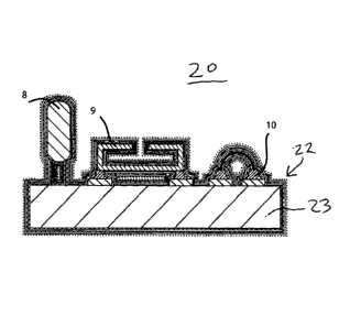
[00011] FIG. I
illustrates an example of components and a substrate of an implantable
medical device 20 with three-dimensional conformal packaging according to the
present
invention. Device 20 includes a plurality of three-dimensional components,
such as transistor 8,
micro-electro-mechanical system 9 and conductive bonding 10, on a substrate 23
which can be
flexible or rigid as desired. A biocompatible multi-layer coating 22 applied
by vapour deposition
conforms to and sealingly covers at least a portion of the components 8,9,10
and the substrate 23.
[00012] The
coating 22 is applied in at least two sets 24, 26, as illustrated
schematically in
FIG. 2, to form coating 22a over component 2 of device 20a with substrate 23a.
Each set has at
least first, second and third layers, such as layers 3, 4 and 5 of set 24. At
least one of the first,
second and third layers consist essentially of a polymer such as parylene and
at least one of the
other two layers of the set consist essentially of inorganic material such
that each layer differs in
at least one diffusion barrier property from the other layers in the set, for
example differing in
diffusion behaviour through each layer relative to the other layers. In some
constructions, the
barrier property for the transport of impurities, such as unwanted molecules,
atoms or ions, both
inward toward a packaged device as well as outward toward a patient in which
the device is
3
CA 02770611 2012-02-08
WO 2011/018709
PCT/IB2010/002197
implanted, is dominated more by the interface between two adjacent layers than
by the thickness
of each individual layer. Preferably, the diffusion behaviour of each layer is
additive to that of
the other layers, and set 26 repeats the same sequence of layers with layers
6, 7, 7' (not shown)
etc. As many sets of layers can be applied as desired. In
some constructions, an additional
treatment, such as a gas plasma, or an additional layer is added to improve
the interface between
two layers, especially with respect to impurity diffusion.
[000131 It is
a realization of the inventors that increasing the number and type of thinner
layers, rather than having fewer, thicker layers, enhances overall barrier
properties of packaging
according to the present invention due to the increased number of layer
interfaces. In other
words, the sum of the interfaces dominates diffusion behaviour, and therefore
the overall barrier
effect of the coating, more than the sum of the thicknesses of the layers.
This may also be
expressed as the diffusion barrier being composed by the layer interface and
each layer itself.
Polymers such as parylene are especially desirable for properties such as
being pin-hole free,
homogenous, and stress-free, and denser materials such as certain inorganic
materials are
especially desirable for their density.
[000141 One
system 100 for achieving such conformal packaging with multi-layer
coatings is shown in FIG. 3. Deposition chamber 103 can be utilized for a
thermal process, such
as a conventional Gorham process, or a plasma enhanced process. For the
thermal process, such
as for parylene deposition, a vaporization chamber 101 is provided to vaporize
a solid parylene
precursor, for example a stable di-cyclic dimer, di-p-xylylene, or halogenated
derivatives at
temperature between 1100 and 200 C. The vaporized precursor then passes to a
pyrolysis
chamber 102 to decompose the dimer in reactive species, such as monomers, at
temperatures
between 400 C and 700 C. For dichloro-p-xylylene, typical parameters are 150 C
for the
vaporization and 650 C for the pyrolysis. The pyrolized precursor then passes
from the pyrolysis
chamber through a gate valve 108 to the medical devices to be treated on a
sample holder 111 in
the deposition chamber 103. Typical parylene layer thickness is between 1 Onm
¨ 100microns.
The precursor vapour pressure in the deposition chamber 103 is approximately
between 1 and 10
Pa, typically 7 Pa, and the substrate temperature is substantially at room
temperature. The
remaining vapour mixture then passes from deposition chamber 103 to a cold
trap 104 connected
to a vacuum pump 105. During the parylene deposition, gate valves 107 and 112
are closed.
4
CA 02770611 2012-02-08
WO 2011/018709
PCT/IB2010/002197
[00015] For
the plasma enhanced process, the deposition process performed in chamber
103 can be either an external downstream plasma enhanced chemical vapour
deposition
(PECVD) facility or an in-situ plasma enhanced process. The downstream reactor
is composed of
a plasma tube 113 and a coil 114 around the plasma tube connected to the RF
generator 115. The
tube 113 is in gaseous communication with the gas source 116 and the
deposition chamber 103.
The desired amounts and proportions of gases supplied by gas source 116
introduced into the
plasma tube 113 may be regulated using one or more mass flow controllers. The
capacitively
and/or inductively coupled high frequency plasma is utilized to excite and/or
dissociate most of
the entering process gas created by organic or inorganic precursors. This
reactive gas is then
injected in the deposition chamber 103 through a valve 112 that is
alternatively opened and
closed in counter phase with the gate valve 108 for parylene deposition.
During the downstream
deposition, the valve 107 is open to evacuate parylene via a bypass 106 to the
cold trap 104. The
power of the generator is between 10 to 500 Watts according to the specific
reactor size.
[00016] For
the in-situ plasma process, controlled plasma is formed adjacent to the
medical device wafers by RF energy applied to sample holder 111 from RF
generator 109, with
the deposition chamber 103 grounded, via a high frequency sealed pass-through
connector 110.
RF generator 109 can supply a high RF frequency of typically 13.56 MHz or 2.45
GHz to the
sample holder 1 1 1 to enhance the decomposition and/or excitation of reactive
species introduced
into chamber.
[00017] In a number of constructions, one of the inorganic layers is SiNx
for its low
permeability and low film stress characteristics. Typically, the deposition
conditions are 130
sccm of SiH4 (5% in argon), 20 seem NH3, 100-180 W RF power, 800 mTorr chamber
pressure,
and 80-120 C substrate temperature. Preferably, thicknesses between 10-300 nm
are deposited.
Other gases could be used, as for example SiH4/NH3/H2 or SiH4/N2.
[00018] In a number of constructions, one of the inorganic layers is SiOx
for its well
established process. Typically, the deposition conditions are 150 sccm SiH4,
100 sccm N20, 30-
80W RF power, 800 mTorr pressure, and 80 C substrate temperature. Preferably,
thicknesses
between 10-300 nm are deposited. Other gases could be used, as for example
SiH4/1\120/Ar or
HMD S/02.
[00019] Other inorganic materials could be used as well according to the
present
invention, with biocompatibility being preferred. Possible materials
including, but not limited to,
5
CA 02770611 2012-02-08
WO 2011/018709
PCT/IB2010/002197
metals, metal oxides, metal nitrides, metal carbides, metal oxynitrides, metal
oxyborides, and
combinations thereof can be utilized. Metals include, but are not limited to,
titanium, aurum,
platinum, argentum, feirum, aluminum, nickel, indium, tantalum, tin,
zirconium, chromium,
zinc, barium, calcium, sodium, alloys thereof, and combinations thereof. Metal
oxides include,
but are not limited to a compound of oxygen and the metals mentioned above and
combinations
thereof. Some examples are titanium oxide, aluminum oxide, calcium oxide,
sodium oxide,
zirconium oxide. Metal nitrides include, but are not limited to a compound of
nitrogen and the
metals mentioned above and combinations thereof. Some examples are aluminum
nitride
titanium nitride. Metal carbides include, but are not limited to a compound of
carbon and the
metals mentioned above and combinations thereof. Metal oxynitrides include,
but are not limited
to a compound of oxygen, nitrogen and the metals mentioned above and
combinations thereof.
Other inorganic materials could be used, but not limited to, are semi-metals,
semi-metal oxides,
semi-metal nitrides, semi-metalcarbides, semi-metal oxynitrides and
combinations thereof.
Preferably materials are, but not limited to, silicon, germanium, boron,
silicon oxide, silicon
nitride, silicon oxynitride, germanium oxide, germanium nitride, germanium
oxynitride, boron
oxide, boron nitride, boron oxynitride and combinations thereof. Other
inorganic biocompatible
materials which can be deposited are calcium phosphate, barium sulfides, and
barium
oxysulfides.
[00020] The
structure of the materials mentioned above could be crystalline, partially
crystalline or amorphous. Preferably amorphous materials are based on, but not
limited to,
silicon, boron, carbon, titanium, aluminum, zirconium and hydroxylapatite and
combinations
thereof.
[00021] Layer
on substrate adhesion or layer on layer adhesion could be improved by
different processes. Typically for parylene adhesion, either on substrate or
on layer, but not
limited to, silanization or gas plasma treatment are used. For example oxygen,
nitrogen or air
plasma is applied directly in the deposition chamber 103 before coating.
Further, other adhesion
layer or plasma enhanced deposition layer can be used. Preferably, a well
known adhesion layer
based on silanes are composed of vinyl trichlorosilane in either xylene,
isopropyl alcohol or a
chlorofluorocarbon gas. Alternatively, gammamethacryloxypropyltrimethoxysilane
in a
methanol-water solvent have been successfully used. Silanes can also be vapour
phase applied if
non-liquid application is preferred.
6
[00022] Thus, while there have been shown, described, and pointed out
fundamental
novel features of the invention as applied to a preferred embodiment thereof,
it will be
understood that various omissions, substitutions, and changes in the form and
details of the
devices illustrated, and in their operation, may be made by those skilled in
the art without
departing from the spirit and scope of the invention. For example, it is
expressly intended that
all combinations of those elements and/or steps that perform substantially the
same function, in
substantially the same way, to achieve the same results be within the scope of
the invention.
Substitutions of elements from one described embodiment to another are also
fully intended and
contemplated. It is also to be understood that the drawings are not
necessarily drawn to scale,
but that they are merely conceptual in nature. It is the intention, therefore,
to be limited only as
indicated by the scope of the claims appended hereto.
7
CA 2770611 2018-08-08