Note: Descriptions are shown in the official language in which they were submitted.
CA 02770719 2016-10-27
-1-
FULLY-CURED THERMALLY OR
ELECTRICALLY-CONDUCTIVE FORM-IN-
PLACE GAP FILLER
FIELD OF THE INVENTION
[0002]
The present invention relates broadly to thermally and/or electrically-
conductive compounds which may be used as gap fillers or caulks between, for
example,
the surfaces of an electronic component and another member, such as a heat
sink or
circuit board, for the conductive cooling and/or the electromagnetic
interference (EMI)
shielding thereof Such compound is provided in the form of a cured polymer gel
component which is blended with a curable resin component and filled with
thermally
and/or electrically-conductive particulates. The invention further relates
to the
application, such as by dispensing through a nozzle or other opening such as a
printing
screen or stencil, of such a compound to one of such surfaces or into a gap
between such
surfaces.
BACKGROUND OF THE INVENTION
[0003]
Circuit designs for modern electronic devices such as televisions, radios,
computers, medical instruments, business machines, communications equipment,
and the
like have become increasingly complex. For example, integrated circuits have
been
CA 02770719 2012-02-09
WO 2011/019719 PCT/US2010/045021
-2-
manufactured for these and other devices which contain the equivalent of
hundreds of
thousands of transistors. Although the complexity of the designs has
increased, the size
of the devices has continued to shrink with improvements in the ability to
manufacture
smaller electronic components and to pack more of these components in an ever
smaller
area.
[0004] As electronic components have become smaller and more densely packed on
integrated boards and chips, designers and manufacturers now are faced with
the
challenge of how to dissipate the heat which is ohmicly or otherwise generated
by these
components. Indeed, it is well known that many electronic components, and
especially
power semiconductor components such as transistors and microprocessors, are
more
prone to failure or malfunction at high temperatures. Thus, the ability to
dissipate heat
often is a limiting factor on the performance of the component.
[0005] Electronic components within integrated circuits traditionally have
been cooled
via forced or convective circulation of air within the housing of the device.
In this regard,
cooling fins have been provided as an integral part of the component package
or as
separately attached thereto for increasing the surface area of the package
exposed to
convectively-developed air currents. Electric fans additionally have been
employed to
increase the volume of air which is circulated within the housing. For high
power circuits
and the smaller but more densely packed circuits typical of current electronic
designs,
however, simple air circulation often has been found to be insufficient to
adequately cool
the circuit components.
[0006] Heat dissipation beyond that which is attainable by simple air
circulation may
be effected by the direct mounting of the electronic component to a thermal
dissipation
member such as a "cold plate" or other heat sink or spreader. The dissipation
member
may be a dedicated, thermally-conductive ceramic or metal plate or finned
structure, or
simply the chassis or circuit board of the device. However, beyond the normal
temperature gradients between the electronic component and the dissipation
member, an
appreciable temperature gradient is developed as a thermal interfacial
impedance or
contact resistance at the interface between the bodies.
CA 02770719 2012-02-09
WO 2011/019719 PCT/US2010/045021
-3-
[0007] That is, and as is described in U.S. Patent No. 4,869,954, the
faying thermal
interface surfaces of the component and heat sink typically are irregular,
either on a gross
or a microscopic scale. When the interfaces surfaces are mated, pockets or
void spaces
are developed therebetween in which air may become entrapped. These pockets
reduce
the overall surface area contact within the interface which, in turn, reduces
the heat
transfer area and the overall efficiency of the heat transfer through the
interface.
Moreover, as it is well known that air is a relatively poor thermal conductor,
the presence
of air pockets within the interface reduces the rate of thermal transfer
through the
interface.
[0008] To improve the heat transfer efficiency through the interface, a pad or
other
layer of a thermally-conductive, electrically-insulating material often is
interposed
between the heat sink and electronic component to fill in any surface
irregularities and
eliminate air pockets. Initially employed for this purpose were materials such
as silicone
grease or wax filled with a thermally-conductive filler such as aluminum
oxide. Such
materials, as may be further described in U.S. Patent Nos. 5,250,209;
5,167,851;
4,764,845; 4,473,113; 4,473,113; 4,466,483; and 4,299,715, usually are semi-
liquid or
solid at normal room temperature, but may liquefy or soften at elevated
temperatures to
flow and better conform to the irregularities of the interface surfaces.
[0009] The greases and waxes of the aforementioned types heretofore known in
the
art, however, generally are not self-supporting or otherwise form stable at
room
temperature and are considered to be messy to apply to the interface surface
of the heat
sink or electronic component. To provide these materials in the form of a film
which
often is preferred for ease of handling, a substrate, web, or other carrier
must be provided
which introduces another interface layer in or between which additional air
pockets may
be formed. Moreover, use of such materials typically involves hand application
or lay-up
by the electronics assembler which increases manufacturing costs.
[0010] Alternatively, another approach is to substitute a cured, sheet-like
material in
place of the silicone grease or wax. Such materials may be compounded as
containing
one or more thermally-conductive particulate fillers dispersed within a
polymeric binder,
CA 02770719 2012-02-09
WO 2011/019719 PCT/US2010/045021
-4-
and may be provided in the form of cured sheets, tapes, pads, or films.
Typical binder
materials include silicones, urethanes, thermoplastic rubbers, and other
elastomers, with
typical fillers including aluminum oxide, magnesium oxide, zinc oxide, boron
nitride, and
aluminum nitride.
[0011] Exemplary of the aforesaid interface materials is are alumina or boron
nitride-
filled silicone or urethane elastomers which are marketed under the name CHO-
THERM and THERM-A-GAPTm by the Chomerics Division of Parker-Hannifin Corp.,
77 Dragon Court, Woburn, MA 01801. Additionally, U.S. Patent No. 4,869,954
discloses a cured, form-stable, sheet-like, thermally-conductive material for
transferring
thermal energy. The material is formed of a urethane binder, a curing agent,
and one or
more thermally conductive fillers. The fillers, which may include aluminum
oxide,
aluminum nitride, boron nitride, magnesium oxide, or zinc oxide, range in
particle size
from about 1-50 microns (0.05-2 mils). Similar materials may be described in
U.S. Pat.
Nos. 5,679,457; 5,545,473; 5,533,256; 5,510,174; 5,471,027; 5,359,768;
5,321,582;
5,309,320; 5,298,791; 5,213,868; 5,194,480; 5,151,777; 5,137,959; 5,060,114;
4,979,074;
4,974,119; 4,965,699; 4,869,954; 4,842,911; 4,782,893; 4,685,987; 4,654,754;
4,606,962;
4,602,678, and in WO 96/37915. Other materials, as may be described in U.S.
Pat. Nos.
6,031,025; 5,929,138; 5,741,877; 5,665,809; 5,467,251; 5,079,300; 4,852,646;
and in
WO 96/05602, WO 00/63968; and EP 643,551, may use a gel or gel-like material
as a
binder or carrier for the filler.
[0012] Sheets, pads, and tapes of the above-described types have garnered
general
acceptance for use as interface materials in the conductive cooling of
electronic
component assemblies such as the semiconductor chips, i.e., dies, described in
U.S.
Patent No. 5,359,768. In certain applications, however, heavy fastening
elements such as
springs, clamps, and the like are required to apply enough force to conform
these
materials to the interface surfaces in order to attain enough surface for
efficient thermal
transfer. Indeed, for some applications, materials such as greases and waxes
which
liquefy, melt, or soften at elevated temperature continue to be preferred as
better
conforming to the interface surfaces under relatively low clamping pressures.
CA 02770719 2016-10-27
-5-
[0013] Recently, phase-change materials have been introduced which are
self-
supporting and form-stable at room temperature for ease of handling, but which
liquefy or
otherwise soften at temperatures within the operating temperature range of the
electronic
component to form a viscous, thixotropic phase which better conforms to the
interface
surfaces. These phase-change materials, which may be supplied as free-standing
films, or
as heated screen printed onto a substrate surface, advantageously function
much like
greases and waxes in conformably flowing within the operating temperature of
the
component under relatively low clamping pressures of about 5 psi (35 kPa).
Such
materials are further described in commonly-assigned U.S. Patent No. 6,054,198
and
Publication No. WO 00/36893 published on June 22, 2000 and entitled "Method of
Applying a Phase Change Interface Material," and are marketed commercially
under the
names THERMFLOW T310, T443, T705, T710, T725, and A725 by the Chomerics
Division of Parker-Hannifin Corp.. Other phase-change materials are marketed
commercially by the Bergquist Company (Minneapolis, MN) under the tradename
"HI-
FLOWTm," by Thermagon, Inc. (Cleveland, OH) under the tradenames "T-PCMTm" and
by Orcus, Inc. (Stilwell, KS) under the tradename "THERMAPHASE." A phase-
change
material/metal foil laminate is marketed by Thermagon, Inc. under the
tradename "T-
MATETm."
[0014] For typical commercial application, the thermal interface material
may be
supplied in the form of a tape or sheet which includes an inner and outer
release liner and
an interlayer of thermal compound. Unless the thermal compound is inherently
tacky,
one side of the compound layer may be coated with a thin layer of a pressure-
sensitive
adhesive (PSA) for the application of the compound to the heat transfer
surface of a heat
sink. In order to facilitate automated dispensing and application, the outer
release liner
and compound interlayer of the tape or sheet may be die cut to form a series
of individual,
pre-sized pads. Each pad thus may be removed from the inner release liner and
bonded to
the heat sink using the adhesive layer in a conventional "peel and stick"
application
which may be performed by the heat sink manufacturer.
[0015] With the pad being adhered to the heat transfer surface of the thermal
dissipation member such as a heat sink or spreader, and with the outer liner
in place to
CA 02770719 2012-02-09
WO 2011/019719 PCT/US2010/045021
-6-
form a protective cover the outer surface of the compound layer, the
dissipation member
and pad may be provided as an integrated assembly. Prior to installation of
the assembly,
the outer release liner is removed from the compound layer, and the pad
positioned on the
electronic component. A clamp may be used to secure the assembly in place.
[0016] Other materials, as exemplified in U.S. Pat. No. 5,467,251, and in
commonly-
assigned U.S. Pat. Nos. 7,208,192 and 5,781,412, and as marketed commercially
by the
Chomerics Division of Parker-Hannifin Corp. under the name "THERM-A-FORMTm,"
are commonly referred to as thermal interface compounds, caulks, form-in-place
materials, or encapsulants. These materials typically are supplied as charged
within one
or more tubes, containers, and the like as, most often, one or two-part liquid
or otherwise
fluent, filled reactive systems which cure at room or elevated temperatures to
be formed-
in-place within the gap or component to which the compound is applied.
Application
may be cartridge or tube guns or other dispensing systems.
[0017] In view of the variety of materials and applications, as exemplified
in the
foregoing, used in thermal management, it is to be expected that continued
improvements
in such materials and applications in thermal management materials would be
well-
received by electronics manufacturers.
BROAD STATEMENT OF THE INVENTION
[0018] The present invention is directed to a thermally and/or electrically-
conductive
compound which is dispensable under an applied pressure as a bead, mass,
pattern, or
other form as issued from a nozzle or as printed through the openings in a
screen or
stencil, or as otherwise dispensable through an orifice. An amount of the
compound,
which may be charged in a tube, cartridge, or other container, may be
dispensed onto a
surface which forms a gap with an opposing, faying, mating, or otherwise
adjoining
surface, or directly into the gap formed between the adjoining surface. As
applied, the
compound forms a bead or mass of material "in place," i.e., in situ. Within
the gap, the
formed-in-place bead or mass of the compound functions as an interface
material in being
CA 02770719 2012-02-09
WO 2011/019719 PCT/US2010/045021
-7-
conformable to at least partially fill the gap and to thereby provide a
thermally and/or
electrically-conductive pathway between the surfaces.
[0019] Unlike more conventional "form-in-place" materials, however, the
compound
of the present invention includes as a major component a substantially fully
cross-linked
or otherwise cured gel component, such as is more fully described in common-
assigned
U.S. Pat. No. 7,208,192. However, by combining a curable resin component with
the gel
component, the compound may be formulated to remain dispensable and soft for
use as a
gel pad or other interface material, but to further cure following dispensing
and deflecting
so as to limit migration between components within an electronic device or
other
application. The combination of the curable resin and gel components,
moreover, allows
for the bead, pad, or other dispensed form of the compound to initially
develop, prior to
or following deflection, a cured outer layer or skin to function as a "resin
dam" for
containing the compound within relatively thick or deep gaps and joints.
[0020] The compound of the present invention as charged within the tube,
cartridge, or
other container, or as otherwise supplied may be stored at room temperature
and does not
require refrigerated or other special storage. The compound also, while being
of a fluent
viscosity which is dispensable under an applied pressure, is generally
viscoelastic and, as
filled, exhibits no appreciable settling of the filler. Such compound also
has, effectively,
an unlimited shelf-life and working time, and can be provided as a one-part
system which
does not require mixing by the user prior to dispensing, or a cure schedule
following
dispensing. The dispensed compound, whether applied as a bead, mass, or other
form, is
generally form-stable and thereby may be handled for assembly similar to a
conventional
molded or extruded strip, pad, sheet, or other pre-form. The dispensed bead or
mass,
moreover, while being form-stable is also extremely soft and conformable
requiring low
or substantially no force in deflection. The compound may be applied using
automated
dispensing equipment, or otherwise applied such with a pneumatically or
manually-
operated applicator gun.
[0021] In an illustrative embodiment, the compound is formulated as being
fluent
under an applied pressure, yet form-stable as applied to a surface or within a
gap, as a
CA 02770719 2012-02-09
WO 2011/019719 PCT/US2010/045021
-8-
blend or other admixture of: (I) a polymer gel component; (II) a curable resin
component;
and (III) a filler which may be thermally and/or electrically-conductive
particles or a
blend thereof. The gel component may be, for example, a thermoplastic gel or a
silicone
gel which may be an organopolysiloxane. The curable resin component may be a
room-
temperature vulcanizing (RTV), moisture-curable silicone resin.
Advantageously, the
compound may be filled, such as to a loading level of between about 20-90% by
total
weight, to exhibit a thermal conductivity of at least about 0.5 W/m-K which is
comparable to that exhibited by current molded or form-in-place materials, but
while still
being dispensable using conventional equipment.
[0022] The present invention, accordingly, comprises the construction,
combination of
elements, and/or arrangement of parts and steps which are exemplified in the
detailed
disclosure to follow. Advantages of the present invention include a
substantially fully-
cured thermal or electrical compound which is dispensable for form-in-place
application,
but which allows for an additional safety margin of "further" curing in-place.
Further
advantages include a soft and conformable compound which has fast, form stable
dispense rates, low-force deflections during assembly and further cure in
application for a
robust, shock and vibration absorbing thermal or electrical assembly. These
and other
advantages will be readily apparent to those skilled in the art based upon the
disclosure
contained herein.
BRIEF DESCRIPTION OF THE DRAWINGS
[0023] For a fuller understanding of the nature and objects of the
invention, reference
should be had to the following detailed description taken in connection with
the
accompanying drawings wherein:
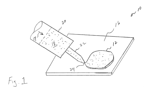
[0024] Fig. 1 is a perspective, somewhat schematic view of a representative
application of the thermally and/or electrically-conductive compound of the
present
invention as dispensed onto a surface;
[0025] Fig. 2 is a cross-sectional view showing a surface, such as the
surface of Fig. 1,
being disposed in opposing a mating surface to form an interface gap
therebetween, with
CA 02770719 2012-02-09
WO 2011/019719 PCT/US2010/045021
-9-
an applied bead, mass, or other form of the compound of the present invention
being
shown to be conformable between the surfaces to at least partially fill the
gap; and
[0026] Fig. 3 is a cross-sectional view showing an alternative application
of the
compound of the invention as a caulk.
[0027] The drawings will be described further in connection with the following
Detailed Description of the Invention.
DETAILED DESCRIPTION OF THE INVENTION
[0028] Certain terminology may be employed in the description to follow for
convenience rather than for any limiting purpose. For example, the terms
"forward,"
"rearward," "right," "left," "upper," and "lower" designate directions in the
drawings to
which reference is made, with the terms "inward," "interior," "inner," or
"inboard" and
"outward," "exterior," "outer," or "outboard" referring, respectively, to
directions toward
and away from the center of the referenced element, and the terms "radial" or
"horizontal" and "axial" or "vertical" referring, respectively, to directions,
axes, planes
perpendicular and parallel to the central longitudinal axis of the referenced
element.
Terminology of similar import other than the words specifically mentioned
above
likewise is to be considered as being used for purposes of convenience rather
than in any
limiting sense. Further, the term "EMI shielding" should be understood to
include, and to
be used interchangeably with, electromagnetic compatibility (EMC), electrical
conduction
and/or grounding, corona shielding, radio frequency interference (RFI)
shielding, and
anti-static, i.e., electro-static discharge (ESD) protection.
[0029] In the figures, elements having an alphanumeric designation may be
referenced
herein collectively or in the alternative, as will be apparent from context,
by the numeric
portion of the designation only. Further, the constituent parts of various
elements in the
figures may be designated with separate reference numerals which shall be
understood to
refer to that constituent part of the element and not the element as a whole.
General
references, along with references to spaces, surfaces, dimensions, and
extents, may be
designated with arrows.
CA 02770719 2012-02-09
WO 2011/019719 PCT/US2010/045021
-10-
[0030] For the illustrative purposes of the discourse to follow, the
thermally and/or
electrically-conductive compound of the invention herein involved is
principally
described in connection with a thermally-conductive formulation. Such
formulation may
be used within a thermal management assembly as a thermal interface material
which
may be dispensed under an applied pressure as a bead, mass, pattern, or other
form as
issued from a nozzle or as printed through the openings in a screen or
stencil, or as
otherwise dispensed through an orifice onto a heat transfer surface of a
thermal
dissipation member such as a heat sink for heat transfer contact with a mating
heat
transfer surface of a electronic component. Such assemblies and thermal
interface
materials therefor are elsewhere described in U.S. Patent Nos. 6,096,414;
6,054,198;
5,798,171; 5,766,740; 5,679,457; 5,545,473; 5,533,256; 5,510,174; 5,471,027;
5,359,768;
5,321,582; 5,309,320; 5,298,791; 5,250,209; 5,213,868; 5,194,480; 5,137,959;
5,167,851;
5,151,777; 5,060,114; 4,979,074; 4,974,119; 4,965,699; 4,869,954; 4,842,911;
4,782,893;
4,764,845; 4,685,987; 4,654,754; 4,606,962; 4,602,678; 4,473,113; 4,466,483;
4,299,715;
and 3,928,907. It will be appreciated, however, that aspects of the present
invention may
find use in other thermal management applications, and in other forms such as
a caulk.
The compound of the invention, as formulated to be additionally or
alternatively
electrically-conductive, also may find use as a form-in-place EMI shielding
material.
Such uses and applications therefore should be considered to be expressly
within the
scope of the present invention.
[0031] In accordance with the precepts of the present invention, a fluent
compound is
provided as exhibiting, in gross morphological aspects, a continuous gel phase
and a
discrete phase of a particulate filler dispersed in the continuous phase. Such
compound,
which is both fluent and viscous or viscoelastic, is especially adapted for
use as a form-
in-place (FIP) thermal interface or EMI shielding gasket material in being
dispensable as
a generally non-slumping or otherwise form-stable bead, mass, or other form
which is
issued from a nozzle or is printed through the openings in a screen or
stencil, or is
otherwise dispensed through an orifice onto the surface of a substrate such as
a heat sink
or electronic component. The bead, mass, pattern or other form so dispensed is
CA 02770719 2012-02-09
WO 2011/019719 PCT/US2010/045021
-11 -
conformal so as to be capable of filling gaps between adjoining surfaces of
the circuitry
components, circuit boards, and housings of electronic devices and electrical
equipment,
or between other adjoining surfaces such as may be found in building
structures and the
like.
[0032] In an exemplary formulation, the compound of the present invention is
formulated as a fluent admixture of: (a) a cured polymer gel component; (b) a
curable
resin component; and (c) a filler component. By "fluent," it is meant that the
admixed
composition exhibits representative fluid flow characteristics allowing it to
be extruded
under pressure through a dispensing nozzle, needle, or other orifice, such as
a printing
screen or stencil, at a given flow velocity. For example, flow rates through a
0.047 inch
(1 mm) orifice of about 2 g/min under an applied pressure of about 90 psi (620
kPa) may
be observed. The compound, moreover, is provided to be sufficiently viscous or
viscoelastic, e.g., about 15 million cps, at about normal room temperature,
i.e., about 25-
30 C, such that the composition may be dispensed from or through a nozzle,
needle,
screen or other orifice as a generally form-stable bead, mass, pattern or
other form. By
"form-stable," it is meant that the quantity of the composition which is
applied to the
substrate exhibits, at steady-state, substantially no appreciable, i.e., 25%
or less, slump,
sag, running, or other flow, at least at temperatures within the range of
normal room
temperature. By "cured" it is meant that the gel component, and, unless
containing a
reactive adjuvant or diluent, the compound itself, does not exhibit, except as
may
normally develop upon aging, further appreciable polymerization, cross-
linking,
vulcanization, hardening, drying, or other like chemical or physical change
such as from
its fluent gel form into a solid or semi-solid form or phase. By "curable" it
is meant that
the resin component undergoes following dispensing and prior to or following
deflection,
further appreciable polymerization, cross-linking, vulcanization, hardening,
drying, or
other like chemical or physical change such as from its fluent viscous or
viscoelastic form
into a solid or semi-solid form or phase.
[0033] Gels useful as the polymer gel component (a) include systems based on
silicones, i.e., polysiloxanes, such as polyorganosiloxane, as well as systems
based on
CA 02770719 2012-02-09
WO 2011/019719 PCT/US2010/045021
-12-
other polymers, which may be thermoplastic or thermosetting, such as
polyurethanes,
polyureas, fluoropolymers, chlorosulfonates, polybutadienes, butyls,
neoprenes, nitriles,
polyisoprenes, and buna-N, copolymers such as ethylene-propylene (EPR),
styrene-
isoprene-styrene (SIS), styrene-butadiene-styrene (SBS), ethylene-propylene-
diene
monomer (EPDM), nitrile-butadiene (NBR), styrene-ethylene-butadiene (SEB), and
styrene-butadiene (SBR), and blends thereof such as ethylene or propylene-
EPDM, EPR,
or NBR. As used herein, the term "polymer gel" is ascribed, in one sense, its
conventional meaning of a fluid-extended polymer system which may include a
continuous polymeric phase or network, which may be chemically, e.g.,
ionically or
covalently, or physically cross-linked, and an oil, such as a silicone or
other oil, a
plasticizer, unreacted monomer, or other fluid extender which swells or
otherwise fills the
interstices of the network. The cross-linking density of such network and the
proportion
of the extender can be controlled to tailor the modulus, i.e., softness, and
other properties
of the gel.. The term "polymer (or silicone as the case may be) gel" also
should be
understood to encompass materials which alternatively may be classified
broadly as
pseudogels or gel-like as having viscoelastic properties similar to gels, such
has by having
a "loose" cross-linking network formed by relatively long cross-link chains,
but as, for
example, lacking a fluid-extender.
[0034] As to silicone gels, particularly-preferred are soft silicone gels
such as marketed
under the name "GEL-8100" by NuSil Technology (Carpinteria, CA). Such gel in
its
cured condition has a penetration value, such as per ASTM D217, of about 100 x
10-1
mm. Other soft silicone gels are marketed under the designation "3-6636" by
Dow
Corning (Midland, MI).
[0035] Resins useful as the curable resin component (b) include moisture-
curable,
room-temperature-vulcanizing (RTV) silicones such as described in U.S. Pat.
Nos.
6,096,413 and 5,910,524. Such silicones may be oxime or other condensation
curing
polymers. The blend of the curable resin component (b) and the cured gel
component (a)
may comprise between about 5-50% by weight of the curable resin component (b)
based
on the total weight of the components (a) and (b).
CA 02770719 2012-02-09
WO 2011/019719 PCT/US2010/045021
-13-
[0036] In accordance with one aspect of the present invention, the blend of
the
polymer gel and curable resin components is rendered thermally-conductive via
its
loading with the filler component (c) which may comprise one or more thermally-
conductive particulate fillers. In this regard, the polymer gel component
generally forms
a binder into which the thermally-conductive filler is dispersed. The filler
is included in
proportion sufficient to provide the thermal conductivity desired for the
intended
application, and generally will be loaded at between about 20-90% by total
weight of the
compound. The size and shape of the filler is not critical for the purposes of
the present
invention. In this regard, the filler may be of any general shape, referred to
broadly as
"particulate," including solid or hollow spherical or microspherical, flake,
platelet,
irregular, or fibrous, such as chopped or milled fibers or whiskers, but
preferably will be a
powder to assure uniform dispersal and homogeneous mechanical and thermal
properties.
The particle size or distribution of the filler typically will range from
between about 0.01-
mil (0.25-250 pm), which may be a diameter, imputed diameter, length, or other
dimension of the particulate, but may further vary depending upon the
thickness of the
gap to be filled. If desired, the filler may be selected as being electrically-
nonconductive
such that compound may be both dielectric or electrically-insulating and
thermally-
conductive. Alternatively, the filler may be electrically-conductive in
applications where
electrical isolation is not required.
[0037] Suitable thermally-conductive fillers generally include oxide,
nitride, carbide,
diboride, graphite, and metal particles, and mixtures thereof, and more
particularly boron
nitride, titanium diboride, aluminum nitride, silicon carbide, graphite,
metals such as
silver, aluminum, and copper, metal oxides such as aluminum oxide, magnesium
oxide,
zinc oxide, beryllium oxide, and antimony oxide, and mixtures thereof. Such
fillers
characteristically exhibit a thermal conductivity of between about 20-50 W/m-
K. For
reasons of economy, an aluminum oxide, i.e., alumina, may be used, while for
reasons of
improved thermal conductivity a boron nitride would be considered more
preferred.
Loaded with the thermally-conductive filler, the compound typically may
exhibit a
thermal conductivity, per ASTM D5470, of at least about 0.5 W/m-K and a
thermal
CA 02770719 2012-02-09
WO 2011/019719 PCT/US2010/045021
-14-
impedance, also per ASTM D5470, of less than about 1 C-in2/VV (6 C-cm2/W),
but as
may vary depending upon the thickness of the compound layer.
[0038] In accordance with another aspect of the present invention, the blend
of the
polymer gel component (a) and the curable resin component (b) is rendered
electrically-
conductive via its loading with an electrically-conductive filler, which may
be provided in
addition to, i.e., a blend, or instead of a thermally-conductive filler. Also,
depending
upon the filler selected, such filler may function as both a thermally and an
electrically-
conductive filler.
[0039] Suitable electrically-conductive fillers include: noble and non-
noble metals
such as nickel, copper, tin, aluminum, and nickel; noble metal-plated noble or
non-noble
metals such as silver-plated copper, nickel, aluminum, tin, or gold; non-noble
metal-
plated noble and non-noble metals such as nickel-plated copper or silver; and
noble or
non-noble metal plated non-metals such as silver or nickel-plated graphite,
glass,
ceramics, plastics, elastomers, or mica; and mixtures thereof. The filler
again may be
broadly classified as "particulate" in form, although the particular shape of
such form is
not considered critical to the present invention, and may include any shape
that is
conventionally involved in the manufacture or formulation of conductive
materials of the
type herein involved including hollow or solid microspheres, elastomeric
balloons, flakes,
platelets, fibers, rods, irregularly-shaped particles, or a mixture thereof.
Similarly, the
particle size of the filler is not considered critical, and may be or a narrow
or broad
distribution or range, but in general will be between about 0.250-250 gm.
[0040] The filler is loaded in the composition in a proportion sufficient
to provide the
level of electrical conductivity and EMI shielding effectiveness within the
gap which is
desired for the intended application. For most applications, an EMI shielding
effectiveness of at least 10 dB, and usually at least 20 dB, and preferably at
least about 60
dB or higher, over a frequency range of from about 10 MHz to 10 GHz is
considered
acceptable. Such effectiveness translates to a filler proportion which
generally is between
about 10-90% by volume or 50-90% by weight, based on the total volume or
weight, as
the case may be, of the compound, and a bulk or volume resistivity of not
greater than
CA 02770719 2012-02-09
WO 2011/019719 PCT/US2010/045021
-15-
about 1 a-cm, although it is known that comparable EMI shielding effectiveness
may be
achieved at lower conductivity levels through the use of an EMI absorptive or
"lossy"
filler such as a ferrite or nickel-coated graphite. As is also known, the
ultimate shielding
effectiveness of member 32 will vary based on the amount of the electrically-
conductive
or other filler material, and on the film thickness.
[0041] Additional fillers and additives may be included in the formulation of
the
compound depending upon the requirements of the particular application
envisioned.
Such fillers and additives may include conventional wetting agents or
surfactants,
pigments, dyes, and other colorants, opacifying agents, anti-foaming agents,
anti-static
agents, coupling agents such as titanates, chain extending oils, tackifiers,
pigments,
lubricants, stabilizers, emulsifiers, antioxidants, thickeners, and/or flame
retardants such
as aluminum trihydrate, antimony trioxide, metal oxides and salts,
intercalated graphite
particles, phosphate esters, decabromodiphenyl oxide, borates, phosphates,
halogenated
compounds, glass, silica, which may be fumed or crystalline, silicates, mica,
and glass or
polymeric microspheres. Typically, these fillers and additives are blended or
otherwise
admixed with the formulation, and may comprise between about 0.05-90% or more
by
total volume thereof.
[0042] The compound may be prepared, for example, in a roll mill or other
conventional mixing apparatus as an admixture of one or more resins or other
polymers
which may also be oligomers or prepolymers, optionally, depending upon the
system, a
cross-linking agent, catalyst, and extender, the filler component, and
optional additive
components. Prior to mixing, the polymer gel component (a) may be subjected to
conditions which polymer, further polymerize, or otherwise cure or convert the
resin,
oligomer, or prepolymer into a fluid or non-fluid extended polymer gel
component. In
this regard, the admixture may be heated, such as in the case of a thermal
addition
polymerization, i.e., vulcanization or cross-linking, system. Alternatively,
the chemical
or physical gellation reaction may be under the influence of atmospheric
moisture, i.e.,
hydrolysis, exposure to ultraviolet (UV) radiation, or other curing mechanism
such an
anaerobic cure.
CA 02770719 2012-02-09
WO 2011/019719 PCT/US2010/045021
-16-
[0043] Depending upon the polymer gel system employed, an inorganic or organic
solvent or other diluent or rheological agent may be added to the mixture of
the
compound to control the viscosity of the final compound which may be adjusted
for the
application equipment or process to be used. As mentioned, the viscosity of
the final
compound typically may be about 15 million cps at about 25-30 C. The compound
may
also be foamed prior to or after mixing, such as under the control of a
physical blowing
agent, such as nitrogen, carbon dioxide, or other gas, or a chemical blowing
agent, which
may be an organic compound or an inorganic compound such as water, which
decomposes or volatilizes to generate a gas. After mixing, the compound may be
charged
into individual tubes, cartridges, or containers and stored for later
application using, for
example, a hand-held applicator gun or syringe, or, alternatively, automated
metering and
dispensing equipment such as a robotic applicator.
[0044] Referring now to the figures wherein corresponding reference characters
are
used to designate corresponding elements throughout the several views with
equivalent
elements being referenced with prime or sequential alphanumeric designations,
an
illustrative dispensed application of the admixed and cured compound of the
present
invention is shown generally at 10 in Fig. 1. In Fig. 1, an amount, 12, of the
compound is
shown as being dispensed under an applied pressure, illustrated by the arrow
14, onto a
primed or unprimed surface, 16, which may be a plastic, metal, or ceramic
surface of, for
example, a heat sink, cold plate, circuit board, housing part, or electronic
component. In
this regard, a supply of the compound, referenced at 18, is shown to be
charged as a one-
part system into a cartridge, tube, or other container, 20, connected in fluid
communication, which may be direct as shown or via hose or other conduit
connected to
a head, with a nozzle, 22, having an orifice, 24. The orifice through which
the amount 12
of the compound is dispensed alternatively may be openings in a screen or
stencil such as
in the case of printing-type dispensing applications.
[0045] Under the applied pressure 14, which may be manually applied using a
gun or
syringe, or developed by air or airless metering equipment such as a
proportioning
cylinder or a pump, a metered amount of the compound may be issued as a pad or
other
CA 02770719 2012-02-09
WO 2011/019719 PCT/US2010/045021
-17-
from nozzle 22 and onto the surface 16. As applied, the amount 12 may be
substantially
self-adherent to the surface 16, such as by surface tension, an inherent tack,
or other
cohesive force. Unlike a grease or the like, the amount 12 advantageously may
be form-
stable at normal room temperature such that part or component to which it is
applied may
be handled for assembly or otherwise. Moreover, unlike conventional form-in-
place
compounds which may bond to the surfaces, the compound of the invention may be
readily cleaned or otherwise removed from the surfaces 16 for repair or
rework.
[0046] Turning now to Fig. 2, an assembly view is shown wherein the surface 16
having the applied amount 12 has been disposed in opposition, or other thermal
adjacency, to a mating surface, 30, which again may be that of a heat sink,
cold plate,
circuit board, housing part, or electronic component, to define a gap,
referenced at 32,
therebetween which may range, for example, from about 2 mils (0.05 mm), or
less, to
about 100 mils (2.5 mm), or more. Within the gap 32, the compound, now
referenced as
the layer 34, may be seen to conform to the surfaces 16 and 30, and to at
least partially fill
the gap 32. Advantageously, the conformal deflection of layer 34 may be
effected under a
relative low or substantially no force, that is, for example, a compression or
force
deflection of about 25% at about 0.3 psi (2 kPa), and of about 50% at about 1
psi (6 kPa)
or less. Prior to following such deflection, a substantially tack-free outer
layer or skin,
represented at 36, initially may be developed about the margin, referenced at
38, of the
layer 34 by virtue of the moisture or other curing of the curable resin
component (b).
Such skin 36, which may form, for example, between about 5-10 minutes
following
application and, in the case of a moisture-cure resin, exposure to atmospheric
moisture,
may be developed by virtue of the initial curing of the curable resin
component (b). Prior
to the further curing of the curable component (b) and resultant increase in
the overall
viscosity of the compound, the skin 36 may function as a "resin dam" to
mitigate the
migration of the layer 34 from between the surfaces 16 and 30.
[0047] Alternatively, the compound forming the layer 34 may be injected
directly into
the gap 32, such as via an opening, referenced in phantom at 40, formed
through one of
the surfaces 16 or 30. Also, and with reference now to Fig. 3, the compound
may be
CA 02770719 2016-10-27
-18-
applied instead as a bead, 40, such as along a seam, 42, within a gap between
adjoining
surfaces 44 and 46. In such application, an initial outer skin, represented at
48, may be
developed over the exterior surface or other margin, referenced at 50, of the
bead 40 prior
to the further curing of the curable resin component (b). Such skin 48
similarly functions
as a "resin dam" to contain the bead 40 within the seam 42.
[0048] As it is anticipated that certain changes may be made in the present
invention
without departing from the precepts herein involved, it is intended that all
matter
contained in the foregoing description shall be interpreted as illustrative
and not in a
limiting sense.