Note: Descriptions are shown in the official language in which they were submitted.
CA 02771015 2012-02-13
WO 2011/018533 PCT/EP2010/061917
CURRENT SENSOR ARRANGEMENT
Field of the invention
This invention relates to a sensor arrangement comprising plural sensor
elements
arranged around a centre point.
Background
In the field of electrical distribution, it is useful to be able to measure
current
flowing through conductors. Often these conductors are operated at high
electric
potential relative to ground and thus it is advantageous to make the
measurement
without direct electrical connection.
It is possible to make such measurements using a current transformer. Such
devices
use a magnetic circuit to couple the current in the conductor to be measured
(primary conductor) and the current in a secondary conductor. This magnetic
circuit typically consists of a yoke of ferromagnetic material having a
conductive
coil (the secondary conductor) wound therearound.
There are a number of drawbacks to this kind of current sensor. The magnetic
circuit may saturate either as a result of impedance in the secondary circuit,
the
presence of a non-time varying current in the primary conductor, or the
presence of
an externally imposed magnetic field. Any of these conditions results in the
current
sensor losing accuracy. Furthermore, hysteresis in the magnetic circuit leads
to
non-linear sensor response at low operating current.
Most modern current sensors can be constructed using surface coils uniformly
spaced around a central cavity through which the primary conductor passes.
These
are known as Rogowski sensors. Rogowski sensors include an air core, rather
than a
magnetic core. Surface coils include one or more turns of a conductor provided
on
a substrate, for example by etching or using printed circuit board technology.
In
order to obtain a good rejection of magnetic fields that are not due to the
primary
conductor, the surface coils are very precisely aligned on axes radial to a
central axis
CA 02771015 2012-02-13
WO 2011/018533 PCT/EP2010/061917
-2-
of cavity through which the primary conductor passes. Such a sensor is
described in
US 6,965,225 B2.
Figure IA is a schematic of a current transformer 10 such as is known in the
art.
The current transformer 10 is interchangeably referred to as a sensor
arrangement
in the following. The current transformer 10 comprises a plurality of sensor
elements 102-1 to 102-6 arranged around a central point through which the
primary
conductor 100 passes when the current transformer 10 is in use. Each of the
sensor
elements 102 comprises one or more turns of a conductive material 104 provided
10 on a substrate 106. A single sensor element 102 is shown in Figure 1B.
The substrates 104, and thus also the sensor elements 102, are aligned
radially with
the central point. Each of the sensor elements 102 is configured such that
when a
magnetic field passes through it a current (also referred to herein as a
signal) is
induced in the sensor element 102. The signal induced due to a magnetic field
passing through in a first direction is positive, while the signal induced by
a
magnetic field passing through in a second opposite direction is negative. The
plural sensor elements 102 which of which the sensor arrangement 10 is
comprised
are arranged such that a circular magnetic field due to the primary conductor
causes
signals of the same sign to be induced in each of the sensor elements 102. As
such,
the signals from each of the sensor elements 102 sums with the signals of the
other
sensor elements 102. In Figure IA a current is flowing through the primary
conductor in a direction into the page, which causes a circular magnetic field
in a
clockwise direction (which is denoted by the dashed circle and arrows).
Sensor arrangements such as that shown in Figure IA exhibit good far-field
performance (i.e. a high level of rejection of fields not due to the primary
conductor) due to the precise radial alignment of the sensor elements, the
equal
spacing of the sensor elements around the centre, and the fact that each
sensor
arrangement has the same configuration as the others.
US 6,965,225 B2 describes a sensor arrangement similar to that of Figure IA.
The
sensor arrangement of US 6,965,225 B2 is adapted so as to be retro-fittable to
an
CA 02771015 2012-02-13
WO 2011/018533 PCT/EP2010/061917
-3-
existing conductor. This involves a mechanical hinge system whereby the sensor
elements can be temporarily separated so as to allow the primary conductor to
be
passed between them.
3 The present invention provides a retro-fittable sensor arrangement which can
require no moving parts and therefore be cheaper to manufacture and less prone
to
mechanical failure than this prior art arrangement.
Summary of invention
A first aspect of the invention provides a sensor arrangement comprising
plural
sensor elements arranged around a centre point, each of the sensor elements
having
a plane of zero sensitivity to uniform magnetic fields, a first one of the
sensor
elements having a first angular separation relative to the centre point from a
second,
adjacent sensor element and having a second angular separation relative to the
centre point from a third, adjacent sensor element, the first angular
separation being
less than the second angular separation,
wherein an intercept of the planes of the first and third sensor elements is
located
outside a triangle formed by the centre point and the first and third sensor
elements
and wherein an intercept of the planes of the first and second sensor elements
is
located inside a triangle formed by the centre point and the first and second
sensor
elements.
The first to third sensor elements may be provided such that each exactly
meets the
conditions:
the first angular separation plus the second angular separation is equal to
2*360 degrees/N, where N is the number of sensor elements; and
an angle between a vector in the plane of the sensor element that is
extending generally towards the centre point and a vector extending from a
centre
of the respective sensor element directly towards the centre point is equal to
N/8
*(the second angular separation minus the first angular separation).
The first to third sensor elements may be provided such that each
substantially
meets the conditions:
CA 02771015 2012-02-13
WO 2011/018533 PCT/EP2010/061917
-4-
the first angular separation plus the second angular separation is equal to
2*360 degrees/N, where N is the number of sensor elements; and
an angle between a vector in the plane of the sensor element that is
extending generally towards the centre point and a vector extending from a
centre
3 of the respective sensor element directly towards the centre point is equal
to N/8
*(the second angular separation minus the first angular separation).
The first sensor element may comprise a first main sensor element and a first
additional sensor element each having the same plane of zero sensitivity that
comprises the plane of zero sensitivity of the first sensor element, a
position of the
first sensor element being constituted by a position of an equivalent dipole
formed
by the first main sensor element and the first additional sensor element when
in use.
The sensor arrangement may comprise plural sensor elements arranged in pairs,
the
angular separation between sensor elements of each pair being less than the
angular
separation between one of the sensor elements of the pair and a closest sensor
element of an adjacent pair of sensor elements.
Brief description of the drawings
Embodiments of the invention will now be described, by way of example, with
reference to the accompanying drawings, in which:
Figure IA depicts a sensor arrangement according to the prior art;
Figure 1B depicts a sensor element of the sensor arrangement of Figure IA;
Figures 2A and 2B depict a sensor arrangement according to a first embodiment
of
the invention;
Figures 3A and 3B depict a sensor device according to the first embodiment of
the
invention;
Figure 4 depicts a sensor arrangement according to a second embodiment of the
invention;
Figures 5A and 5B illustrate components of the sensor arrangement of Figure 4;
and
Figures 6A and 6B depict a sensor device according to the second embodiment of
the invention.
CA 02771015 2012-02-13
WO 2011/018533 PCT/EP2010/061917
-5-
Detailed description of the embodiments
In the above-mentioned drawings and below-described embodiments, like
reference
numerals refer to like elements throughout.
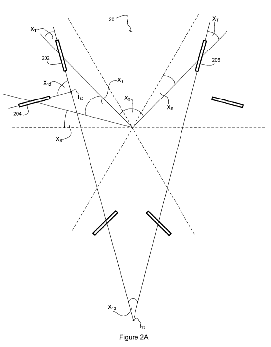
Figure 2A shows a sensor arrangement 20 according to a first embodiment of the
invention.
The sensor arrangement 20 according to the first embodiment of the invention
includes a plurality of sensor elements 202, 204, 206 etc. which may be
similar to
that depicted in Figure 113. The sensor elements 202, 204, 206 etc. are
arranged
around a centre point. The sensor arrangement 20 is operable to detect a
current
flowing through a primary conductor which passes near the centre point in a
direction substantially perpendicular to the page. Each sensor element 202,
204,
206 etc. has zero sensitivity to uniform magnetic fields which are parallel to
a plane
that passes through the sensor element 202, 204, 206 etc. . Hereafter, these
planes
are referred to as planes of zero sensitivity to uniform magnetic fields, or
simply
planes of zero sensitivity.
The inventors have discovered that the sensor elements 202, 204, 206 etc. can
be
placed around the centre point at unequally spaced locations whilst achieving
far-
field performance comparable to that exhibited by the prior art sensor
arrangement
of Figure IA. However, in order to achieve this, the positions and alignments
of
the sensor elements 202, 204, 206 etc. if the of the coils must are adjusted
generally
according to a specific relationship.
In Figure 2A, the dashed lines represent radial axes having equal angular
separation
upon which the sensor elements 102 of the prior art sensor arrangement 10 of
Figure IA were located. It can be seen from Figure 2A that each of the sensor
elements 202, 204, 206 etc. of the arrangement 20 according to the first
embodiment has been displaced from the equally spaced locations of the sensor
elements 102 of the prior art sensor 10. The angle by which the position of a
sensor
element 202, 204, 206 etc. is shifted from its respective location in the
prior art
sensor arrangement 10 is hereafter called the shift angle Xs.
CA 02771015 2012-02-13
WO 2011/018533 PCT/EP2010/061917
-6-
In the prior art arrangement 10 of Figure IA each of the sensor elements 102
is
arranged such that the plane of zero sensitivity of the sensor element 102 is
aligned
with a radial axis extending from the centre point. In other words, a plane of
the
substrate on which the sensor element is provided is radial to the centre
point of
the prior art arrangement 10.
In the sensor arrangement of Figure 2A, however, the sensor elements 202, 204,
206
etc. are not aligned with the radial axes upon which they are located. In
other
words, the plane of zero sensitivity of the sensor element is at an angle to
the radial
axis upon which its centre lies. In this example, the plane of the substrate
on which
the sensor element is provided is the same as the plane of zero sensitivity.
Put
another way, the sensor element has a plane that is the same as the plane of
zero
sensitivity. Consequently, in this example, the plane of the substrate on
which the
sensor element is provided is at an angle to the radial axis upon which its
centre lies.
The angle between a vector in the plane of zero sensitivity of a sensor
element 202,
204, 206 etc. pointing generally (or most) towards the centre point and a
vector
aligned with the radial axis and pointing towards the centre point is
hereafter called
the tilt angle XT.
A general relationship between the positions and orientations of the sensor
elements 202, 204, 206 etc. in an N-sensor arrangement, which maintains the
same
level of far-field performance as the prior art arrangement 10 can be
described with
reference to three adjacent sensor elements, hereafter referred to as the
first sensor
element 202, the second sensor element 204, and the third sensor element 206.
As can be seen in Figure 2A, the first sensor element 202 is separated from
the
second sensor element 204 by a first angular separation X, relative to the
centre
point. The first sensor element is separated from the third sensor element 206
by a
second angular separation Xz relative to the centre point.
CA 02771015 2012-02-13
WO 2011/018533 PCT/EP2010/061917
-7-
In the sensor arrangement 20, the following three criteria are true. Meeting
these
criteria allows the sensor arrangement 20 to exhibit the same level of far-
field
performance as the prior art sensor arrangement 10.
3 1) The second angular separation Xz is larger than the first angular
separation X,;
2) An intercept I13 of the planes of zero sensitivity of the first and third
sensor elements is located outside a triangle formed by the centre point
and (centre points of) the first and third sensor elements 202, 206; and
3) An intercept I,Z of the planes of zero sensitivity of the first and second
sensor elements 202, 204 is located inside a triangle formed by the centre
point and (centre points of) the first and second sensor elements 202,
204.
13 Described another way, the three above criteria are as follows:
1) The second angular separation Xz is larger than the first angular
separation
X,;
2) An angle XTI2 between a vector in the plane of the first sensor element 202
which extends generally towards the centre point and a vector in the plane of
the second sensor element 204 that extends generally towards the centre
point is greater than the first angular separation X1; and
3) An angle XTI3 between a vector in the plane of the first sensor element 202
that extends generally towards the centre point and a vector in the plane of
the third sensor element 206 that extends generally towards the centre point
is less than the second angular separation X2.
More specifically and optimally, the relationship between the tilt angle XT
and the
shift angle Xs is given by:
XT = N X Xs/2 [EQUATION 1]
Where N is the number of sensor elements, which in this example is 6.
CA 02771015 2012-02-13
WO 2011/018533 PCT/EP2010/061917
-8-
The tilt angle XT can also be defined with reference to the first and second
angular
separations X,, Xz (assuming the above criteria are satisfied), as can be seen
below:
3 XT = N X (X2, - X1)/8 [EQUATION 2]
The application of the shift angle Xs and the tilt angle XT allows the
distance
between two adjacent sensor elements 202, 206 to be increased relative to the
distance between two adjacent sensor elements 102 of the equally spaced sensor
arrangement of Figure IA in the prior art. This can most clearly be seen in
Figure
2B in which the sensor elements 102 of the prior art arrangement 10
corresponding
to the first and third sensor elements 202, 206 of arrangement 20 of the first
embodiment are shown (in broken lines) in conjunction with the arrangement 20
of
the first embodiment. The distance Al between the prior art sensor elements
102 is
13 clearly smaller than the distance A2 between the first and third sensor
elements 202,
206 of the arrangement 20 of the first embodiment. Consequently, the invention
allows a sensor device to be constructed which can be applied to a conductor
(that
would normally be insulated) without moving parts and without the need to
interrupt the current flow in the primary conductor.
Figures 3A and 3B depict a plan- and side-view respectively of a sensor device
300
according to the first embodiment of the invention.
The device comprises the sensor arrangement shown in Figure 2A and 2B. The
arrangement of sensor elements 202, 204, 206 etc. is provided in a rigid frame
302.
The rigid frame comprises top and bottom portions 302-1, 302-2 which may be
connected together, for example using a plastic bolt or bolts (not shown)
which
pass(es) from the top portion 302-1 to the bottom portion 302-1 of the frame.
The
frame 302 may have slots formed in inner surfaces of the top and bottom
portions
302-1, 302-2 for supporting the edges of the substrates of the sensor elements
202,
204, 206 etc. Alternatively the edges of the substrate boards are held against
the
inner surfaces of the top and bottom portions 302-1, 302-2 of the frame.
According to alternative embodiments, the substrates are insert moulded. The
CA 02771015 2012-02-13
WO 2011/018533 PCT/EP2010/061917
-9-
sensor device of Figure 3A and 3B may also include signal conditioning
components
(not shown) provided on the substrates.
When in use, the device Figure 3 is moved towards a subject conductor, the
current
3 flowing through which is to be measured, until the conductor passes through
the
aperture denoted A. The magnetic field due to the conductor cause signals to
be
induced in the sensor elements 202, 204, 206 etc, which allows the current
flowing
through the conductor to be measured. By supporting the device 300 such that
the
conductor is within the volume bounded by the sensor elements, the device 300
can
be used accurately to measure current flowing in the conductor.
Alternatively, the sensor elements could be located such that their tilt
angles deviate
by a small extent from the criteria stated above. Deviations from the criteria
stated
above reduce far field performance. However, advantages that arise from having
a
13 design that is simple and inexpensive to manufacture may outweigh a small
performance reduction in many instances. Advantageously, the criteria above
are
met in a design. Alternatively, the angle criteria may be deviated from by a
relatively small amount. In this case, additional design features may be
included
such as to compensate for performance changes resulting from the deviation.
Figure 4 depicts a sensor arrangement according to a second embodiment of the
invention. In this embodiment, not all of the criteria stated above are met.
The sensor arrangement 40 of Figure 4 comprises eight sensor elements (denoted
by
the hashed areas on the Figure). These are positioned relative to one another
and
aligned relative to the centre point either exactly or closely according to
the
relationships described with reference to Figure 2A.
Two sensor elements are provided on each of two extending substrate members
402-1, 402-1. One sensor element is provided on each of four smaller substrate
members 404-1, 404-2, 404-3, 404-4. The sensor elements are arranged such that
the signals induced due to a circulating magnetic field sum with one another.
CA 02771015 2012-02-13
WO 2011/018533 PCT/EP2010/061917
-10-
The two extending substrate members 402-1, 402-2 are arranged substantially
parallel to one another. Two of the smaller substrate members 404-1, 404-4 lie
in a
first plane and the other two of the small substrate members 404-2, 404-3 lie
in a
second plane. The first and second planes are substantially parallel to one
another
and substantially perpendicular to the planes of the extending substrate
members
402-1, 402-2. The provision of two sensor elements on a single substrate
allows for
easier and more precise alignment and manufacture of the sensor arrangement
40.
Figure 5A shows an example of the extending substrate members 402 and the
small
substrate members 404.
The extending substrate boards include at each end one or more turns of a
conductor, which form the sensor elements 402-A, 402-B. The sensor elements
402-A, 402-B on the extending sensor member are oppositely-configured (i.e.
oppositely coiled or wound). As such, signals induced in the sensor elements
402-
A, 402-B due to a uniform (or far) field passing through the extending sensor
member cancel such that the net signal between the two sensor elements is
zero.
The small substrate board may be substantially as described with reference to
Figure
1B.
The tilting and movement of the sensor elements (as described with reference
to
Figure 2A and 2B and exhibited by the arrangement of Figure 4) relative to the
equally spaced radial arrangement of the prior art maintains the far-field
performance compromises the uniformity of sensitivity to current flowing
through a
conductor 100 provided across the sensing volume. However, this can be
corrected
for by introducing additional sensor elements into the sensor arrangement.
Figure 5B shows a one of the extending substrate boards of the embodiment of
Figure 4 including additional sensor elements 500. The additional sensor
elements
500, which are additional to the main sensor elements 402-A and 402-B have an
effect of correcting the uniformity of sensitivity. This aspect is described
and
CA 02771015 2012-02-13
WO 2011/018533 PCT/EP2010/061917
-11-
claimed in a co-pending application filed on even date herewith to the same
applicant, the contents of which are incorporated by reference.
The additional sensor elements 500 also have an effect of moving the position
of a
3 dipole provided by the main sensor elements 402-A, 402-B. The main sensor
elements are modified to account for the additional sensor elements. In
particular,
the number of turns of conductor material of the main sensor elements may be
modified to maintain a similar turn area to a non-compensated design. Also,
the
position of the main sensor elements is modified to maintain the effective
dipole
position of an uncompensated design. The person skilled in the art will know
how
to calculate main and additional sensor elements parameters and locations in
order
to achieve a particular design requirement.
Figures 6A and 6B show a sensor device 60 according to the second embodiment
of
the invention in situ around the conductor.
The device 60 comprises the sensor arrangement 40 shown in Figure 4. The
arrangement of sensor elements 404, 402 is provided in a rigid frame 600. The
rigid
frame 600 comprises top and bottom portions 600-1, 600-2 which may be
connected together, for example using a plastic bolt or bolts (not shown)
which
pass(es) from the top portion 600-1 to the bottom portion 600-1 of the frame.
The
frame 600 may have slots formed in inner surfaces of the top and bottom
portions
600-1, 600-2 for supporting the edges of the substrates of the sensor elements
404,
402. Alternatively the edges of the substrate members may be held against the
inner
surfaces of the top and bottom portions 600-1, 600-2 of the frame. According
to
alternative embodiments, the substrates members are insert moulded. The sensor
device of Figure 6A and 6B may also include signal conditioning electronics
(not
shown) provided on the substrates.
Locations of the sensor elements in the figures 4 and 6 embodiments are such
that
they meet the criteria stated above in relation to the Figures 2 and 3
embodiments,
but may not strictly meet the terms of the equations provided above. The
locations
of the sensor elements on the extending substrate members 402-1 and 402-2 is
CA 02771015 2012-02-13
WO 2011/018533 PCT/EP2010/061917
-12-
defined by the distance between the centres of the sensor elements on each
board
and by the separation of the extending substrate members. The locations of the
smaller substrate members 404-1, 404-4 is selected such that the sensor
elements
supported by those members are symmetrical to the sensor elements supported on
the extending substrate members 402-1 and 402-2.
With the boards of Figure 5B additional sensor elements 500 are provided on
the
402-1 and 402-2 with parameters (e.g. number of turns) and positions such as
to
move the positions of the dipole in effect provided by the combinations of the
main
sensor elements 402 and the additional sensor elements 500 so that the terms
of the
equations are met, or at least are substantially met. The additional sensor
elements
500, by moving the dipole, also adjust the tilt angle XT and the shift angle
XF.
Parameters of one example are as follows:
For the sensor elements 404, turns of conductive material with areas of 625mm
are
positioned at of 32mm from tangent position.
For elements 402, turns of conductive material with areas 855mm squared at
29mm
from tangent position. The additional sensor element 500 comprises turns of
conductive material with areas negative 340mm squared (because the conductive
material is oppositely would) at 18mm from tangent position and turns of
conductive material with areas 110mm squared at 12mm from tangent position.
The sum of the turns area of the element 402 and the additional sensor element
500
is 625mm squared, which is the same as the turns area of the sensor element
404.
The equivalent dipole position is given by averaging the positions weighted by
the
turn area product. The equivalent position is therefore (855*29-
340*18+110*12)/(
855-340+110) = 32mm.
CA 02771015 2012-02-13
WO 2011/018533 PCT/EP2010/061917
- 13-
This gives rise to values as follows:X, is 30.4 degrees, Xz is 59.6 degrees,
X.13 is zero
degrees (because the sensor elements are parallel) and X.12 is 90 degrees. XT
is 29.8
degrees, and Xs is 7.3 degrees.
As such, the terms of the equations are substantially met.
According to some embodiments of the invention, sensor devices including eight
sensor elements each spaced 35mm from the centre point can exhibit 16 nodes in
the far-field response and 16 planes of uniform sensitivity dipole while at
the same
time providing a clear aperture of 35mm through which the primary conductor
can
be passed.
The number of sensor elements advantageously is even, formed in at least two
sets
each of two sensors. However, the number of sensor elements may alternatively
be
odd.
It should be realized that the foregoing embodiments should not be construed
as
limiting. Other variations and modifications will be apparent to persons
skilled in
the art upon reading the present application. Moreover, the disclosure of the
present application should be understood to include any novel features or any
novel
combination of features either explicitly or implicitly disclosed herein or
any
generalization thereof and during the prosecution of the present application
or of
any application derived therefrom, new claims may be formulated to cover any
such
features and/or combination of such features.