Note: Descriptions are shown in the official language in which they were submitted.
CA 02771156 2012-02-14
WO 2011/018521 PCT/EP2010/061850
1
MICRO MECHANICAL ELEMENT
The invention relates to a micromechanical element, in particular, an
adjustable optical
spectral filter and a method to produce this which, according to prior art,
can be realised
with the help of a row of alternately movable and fixed optical
micro/reflectors,
particularly where the reflectors have a diffractive or light deflecting
effect.
BACKGROUND TO THE INVENTION
Movable optical micro reflectors used for spectral filtering have been
described
previously in, among others, the international patent application no. WO
2004/059365,
which relates to diffractive optical elements that can be configured, that
comprise a
series of movable diffractive micro reflectors that go by the name diffractive
sub-
elements. The reflectors or the sub-elements (1,3, See figures Oa and Ob) have
lateral
dimensions considerably larger than the displacement, and can have the shape
of
rectangles (Figure Oa) or sectors of concentric rings (Figure Ob). Light
reflected from
the different sub-elements will interfere, so that one can filter out light of
a certain
spectral composition, and by adjusting the position of the elements vertically
or
laterally, one can continuously change the characteristics of the filter.
A special case of the mentioned configurable diffractive elements can be made
up of a
row where every other reflector can be moved in synchrony and take up two
different
positions, while the other reflectors are stationary. This results in an
optical filter that
can alternate between two states: A simple band pass filter and a double band
pass filter
where the bands lie on their own side of the simple filter. A such alternating
filter is
very well suited to applications within spectroscopy and infrared gas
measurements in
particular. A practical embodiment of the filter as a micro-opto-
electromechanical
system (MOEMS) must meet certain requirements. The positions of the movable
reflectors must be adjustable over a distance of a quarter of a wavelength in
a direction
perpendicular to the optical surfaces. The wavelength is in the infrared area
so that the
displacement is of the order of I micrometre. The reflectors must lie in the
same plane.
The displacement shall be in synchrony and be able to be repeated,
particularly with a
frequency in the kilohertz area, and with billions to trillions of cycles
within the lifetime
RECTIFIED SHEET (RULE 91) ISA/EP
CA 02771156 2012-02-14
WO 2011/018521 PCT/EP2010/061850
2
of the components. Between the movable reflectors there shall be fixed
reflectors which
in form and size are approximately similar to the movable reflectors. The
reflectors are
given diffractive properties in that they are engraved with a relief pattern
where the
depth of this pattern is of the same order of magnitude as the wavelength. A
total area of
several square millimetres ought to be covered by reflectors moving in
synchrony.
The optical principle for the alternating filter described above is regarded
as prior art
and a concrete micromechanical shape has been published previously in an
article by
Hikon Sagberg et al "Two-state Optical Filter Based on Micromechanical
Diffractive
Elements" presented at IEEE/LEOS International Conference On Optical MEMS and
Their Applications in August 2007 (OMEMS2007). Figure Oc shows an embodiment
according to prior art, based on a commercially available silicon wafer,
comprising a
substrate and a structural layer which are fused together with a thin layer of
silicon
dioxide fte the di ffract ve opticall surfaces are formed at the top of the
structural
layer, this is divided up into two sets of beams (1,3) with the help of an
etching method.
Thereafter, every other beam (3) is made movable by etching away the layer of
oxide in
selected areas. This is a simple process, but has three essential
disadvantages. Firstly,
holes must be made in the movable beams so that the gas or the liquid which is
used for
the etching of the layer of oxide shall be able to enter into it. Secondly,
surfaces with
different electrical potential will come into contact when the beams are
pulled into the
substrate, and the electrical current that passes between the surfaces can
lead to a large
drop in voltage, or result in the beams being fused together with the
substrate with the
help of the electrical current between them. Thirdly, the contact area between
the beams
and the substrate becomes large and unpredictable, something which can lead to
stiction. Stiction occurs when the adhesive forces between two surfaces become
so large
that the available forces that are set up do not manage to pull the surfaces
apart, and a
lasting, unwanted adhesion arises. In this case, the forces that are set up
come from
elastic bridges in silicon.
To reduce the adhesive forces and avoid stiction, there are several known
methods used
on different types of electromechanical systems. Particularly important is the
use of
spacer blocks, also referred to as "landing pads", "stops", "bumps" or
"dimples". These
RECTIFIED SHEET (RULE 91) ISA/EP
CA 02771156 2012-02-14
WO 2011/018521 PCT/EP2010/061850
3
shall, as a rule, satisfy two functions: To define an accurate distance as an
end stop for
one movement, and to prevent stiction by making sure that large areas do not
come into
contact. See, for example, US 2001/005583 1, US 6,437,965, US 6,528,887. Other
important techniques for stiction prevention are:
- to avoid that surfaces with different electric potential come into contact,
- to avoid that a parasitic charging of dielectric materials take place,
- to treat the surfaces chemically or mechanically to introduce roughness and
reduce the
contact area, and
- to treat the surfaces chemically to increase their water repellent
characteristics,
- to wrap the electromechanical system hermetically to avoid moisture, so that
the water
repelling characteristics of the surfaces become less important.
The existing solutions are, to a large extent, adapted to the specific needs
of the
individual micromechanical systems, and there are no standard methods. Some
typical
problems with the existing solutions are that:
The manufacturing method can be very complicated when one must use spacer
blocks,
the form of the spacer blocks can come to affect the above-lying optical
surfaces (in
particular with the use of so called surface micro-machining with a deposited
structural
layer), chemically treated water repellent surfaces can change characteristics
with time,
and a possible generation of surface roughness can come to damage other
critical
surfaces in the system than the surfaces which shall get a reduced contact
area.
An example of an MEMS which is very successful, but also very complicated, is
the
DMD mirror matrices that are produced by Texas Instruments and which are
described
in, for example, US 7,411,717 and more specifically with regard to the
problems related
to stiction in US2009/0170324. In the manufacture of this product many of the
methods
described above are used.
The problem with producing spacer blocks and at the same time avoiding
roughness of
the surfaces which later shall be joined together or be laminated is
considered in, among
others, US2009/0 1 703 1 2. There are several disadvantages of the method
presented in
US2009/0170312. The under-etching process is difficult to control, therefore
there is a
RECTIFIED SHEET (RULE 91) ISA/EP
CA 02771156 2012-02-14
WO 2011/018521 PCT/EP2010/061850
4
practical limit on the minimum reproducible lateral size of the anti-bonding
stops. Also,
the surfaces of the anti-bonding stops will be relatively smooth, which is a
disadvantage
if bonding shall be prevented. Further, the oxidation process will alter the
top surface as
well as the cavity, restricting the use of diffractive surfaces instead of
plane mirrors.
Many of the prior art examples with spacer blocks use a so called sacrifice
layer. During
the manufacture of the micro system, the sacrifice layer lies between what
shall become
movable micro structures and fixes these. The sacrifice layer is often made
from silicon
dioxide, but can also be made from a different material, for example, a
polymer. The
sacrifice layer is removed towards the end of the processing with the help of
etching. A
challenge with the removal of the oxide layer can be to get the etching
process to be
sufficiently selective, so that it removes the sacrifice layer only and no
other material. A
further two challenges arise if an etching liquid must be used: To get the
liquid to
penetrate into the micro cavities, and to get the cavities dry after the
etching.
EP 1561724 presents an accelerometer where dimples may be included on the
bottom of
a recess in order to prevent stiction. However, there is no hint to how these
dimples may
be realized. Creating fine structures on the bottom surface of large KOH or
TMAH
etched recesses is very difficult, especially when standard MEMS production
equipment
is used.
US 6,528,887 presents a medium complex method to manufacture the spacer blocks
on
the underside of a structural layer. Such layers normally consist of silicon,
and in
MEMS terminology they are referred to as device layers. In the introduction of
said
patent (2-8) it is claimed that it is generally not possible to process the
underside of a
MEMS device layer to form spacer blocks before this is laminated with a
substrate.
Furthermore, it is referred to how spacer blocks can be formed by processing
from the
top side of the device layer, together with the use of a sacrifice layer
between the
substrate and the device layer (an often used method).
The object of the present invention is to provide a micromechanical unit and a
method
for producing the micromechanical unit, the unit being cheap in production and
easy to
RECTIFIED SHEET (RULE 91) ISA/EP
CA 02771156 2012-02-14
WO 2011/018521 PCT/EP2010/061850
control having reduced stiction between the moveable beams. This is provided
with a
unit and method as stated above being characterized as stated in the
independent claims.
The present invention thus provides a practical method to construct a such
row, where
5 in the preferred embodiment the fixed and movable optically reflecting
surfaces are
made up of the top sides of fixed and movable beams that are etched out from
one and
the same material layer. The fixed beams are permanently connected to a
substrate via a
thin dielectric layer, while the movable beams span across etched recesses in
the
substrate. They can thereby be pulled down towards the substrate by an
electrostatic
force until the bottom of the beams meet spacer blocks at the bottom of the
recesses.
The spacer blocks are shaped to give a small contact area and thus weak
adhesive
forces, something that ensures that the movable beams can return to the
starting point
when the electrostatic force ceases to function, and is made and machined from
the
same dielectric layer fixing the fixed beams to the substrate.
In the description that follows it is shown that it is actually possible, in a
practically
feasible and relatively simple way, to form spacer blocks by processing the
top side of
the substrate and/or the underside of the device layer before the joining
together/lamination, in such a way that one achieves both good lamination
characteristics and good, stiction-free spacer blocks. The solution which is
presented is
particularly well suited to form rows of altematingly fixed and movable
structures.
The invention will be described below with reference to the accompanying
drawings,
illustrating the invention by way of examples, wherein
Figures Oa,b illustrates the prior art as disclosed in abovementioned
W02004/059365
Figure Oc illustrates the principle of the prior art.
Figure 1 a,b illustrates the preferred embodiment of the present invention.
Figure 2 illustrates an alternative embodiment of the present invention.
Figure 3 illustrates an an embodiment of the present invention as seen from
above.
Figure 4 illustrates a detail of the embodiment illustrated in figures 1 a,b.
Figure 5a-h illustrates the production method according to the preferred
embodiment
of the invention.
RECTIFIED SHEET (RULE 91) ISA/EP
CA 02771156 2012-02-14
WO 2011/018521 PCT/EP2010/061850
6
The invention thus comprises a new method for the manufacture of a micro
electromechanical system that functions as an alternating optical filter as
described in
the above mentioned article in OMEMS2007. Central to the new method is the use
of a
substrate and a thinner layer of material, generally with a thickness of the
order of 5-
50 m, both preferably made from silicone, which are prepared in such a way
that when
they are joined together, some areas will have maximum adhesion, and other
areas will
have minimal adhesion. In the areas with minimal adhesion, spacer blocks are
used to
reduce the adhesive forces and avoid stiction.
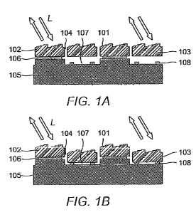
Referring to figure 1 a and 1 b the fixed and movable optical micro reflectors
(101)
mentioned in the introduction are made up of the top side of the fixed (102)
and
movable beams (103) that are cut/machined/etched out from a material layer.
The
beams are illustrated as straight, but can also have other shapes as shown in
the above
mentioned WO publication. The fixed beams are permanently connected to a
substrate
(105) via a thin dielectric layer (106), while the movable beams are spanning
out over
etched recesses (107) in the substrate. Thereby, they can be pulled down
towards the
substrate by an electrostatic force until they are stopped by the spacer
blocks (108),
which can be at the bottom of the recesses or on the underside of the beams
(as shown
in Figure 2). An essential feature of the present invention is that the spacer
blocks are
made from the same dielectric layer that fastens the fixed beams to the
substrate. The
spacer blocks are shaped to give a small contact area and thus weak adhesion
forces,
something which ensures that the movable beams can be returned to their
initial position
when the electrostatic force ceases to function. Thus the incoming light L may
be
manipulated by the diffractive patterns depending on the relative positions of
the beams.
Using contact lithography and anisotropic etching the diameter of the spacer
blocks can
be made less than a micrometer, and using a so-called stepper or reduction
lithography
it is in principle possible to obtain dimensions less than 100nm.
The force that makes the beams return to their initial position is in one
embodiment of
the invention (shown in Figure 3) generated in that the movable beams (303)
are
RECTIFIED SHEET (RULE 91) ISA/EP
CA 02771156 2012-02-14
WO 2011/018521 PCT/EP2010/061850
7
connected together to a common (movable) frame (304), and this frame is
connected to
a fixed, outer area (302) via small, elastic bridges (springs) (305). These
springs will be
bent when the frame is moved and thus create an upwardly directed force that
attempts
to bring the frame back to its starting position. To move the frame with the
optical
surfaces the desired distance away from the starting position an electrostatic
field is
used that is created by applying a voltage between the substrate and the
device layer and
thereby, at least, the movable beams. If the voltage is sufficiently high, the
frame will be
pulled all the way in to the spacer blocks that lie in the recesses in the
substrate, as
shown in Figure 1 B.
The invention provides a simple and robust solution for the mechanical
challenge that
lies in the displacement of the optical surfaces. The combination of the
process steps
that are described in detail below ensures that:
1) TIP desired displacement distance can be determined freely via the depth
of the etched recesses,
2) The contact area is reduced on a nano scale in that the etching creates a
rough surface,
3) The contact area is reduced on a micro scale in that the extension of the
spacer blocks is made as small as possible,
4) Good fixed adhesion to the fixed beams is ensured, by, for example,
protection of the chosen polished surfaces during the etching,
5) The form, thickness and location of the spacer blocks can be freely
determined without the optical surfaces being affected,
6) The optical surfaces lie on the top side of thick beams which are
approximately free for internal mechanical tensions,
7) The micro system can be completed without the complicated removal of a
"sacrifice" layer, as is often the case in known methods, for example, as
shown in Figure OC.
Figure 4 shows in greater detail the difference between the surface of the
substrate (401)
under a fixed (402) and a movable (403) beam. The substrate has initially a
smooth
(polished) surface (404) as shown below the dielectric layer (405). The
etching of the
RECTIFIED SHEET (RULE 91) ISA/EP
CA 02771156 2012-02-14
WO 2011/018521 PCT/EP2010/061850
8
recesses will result in a rougher surface (406) and this roughness is largely
kept after the
deposition or growth of the dielectric layer that is to become the spacer
blocks (407). It
can be an advantage that the spacer blocks have a rough surface to further
reduce the
contact area and the adhesive forces. Consequently, the total contact area
between the
spacer blocks ought to be as small as possible, preferably less than 1%, but
they must
also be sufficiently large so that they do not yield too much when the beams
are placed
against them and have a distribution along the beams that prevents the bending
of these.
The dielectric layer that lies on the substrate outside the recesses will have
a much
smoother surface than the spacer blocks as it is formed on top of a polished
surface.
Here, it is desirable to have a large adhesive force/energy to achieve a good
joining
together with the static parts of the structural layer.
Even if the same dielectric layer can form both the joined together layer and
the spacer
blocks, the previous etching process can give the surface of the layer
different
characteristics in the two areas.
In a preferred embodiment (Figures 5A-H), the invention comprises a method
where
one starts with a substrate (105) which has a polished top side
(Figure 5A). Recesses (107) are etched into the substrate with a depth that
corresponds
to the displacement distance of the beams (Figure 5B), for example, 830 nm, if
light
with a wavelength of around 3.3 m shall be measured, for example, in the
measuring
of methane or other hydrocarbons, but adapted to about '/4 of the wavelength
of the light
the element shall be used on. The etching process can be a reactive ion
etching with a
mixture of SF6 and C4F8 and with a calibration of the etching time one can
achieve a
depth accuracy of the order of 5%. Thereafter, a dielectric layer (501) is
deposited, or
grown, for example, thermally grown silicone dioxide, which thereafter is
etched away
in some areas to form the spacer blocks (108) (Figures 5C-D). Figure 5E shows
how the
device layer (502) is fused together with the substrate (105) with the help of
a wafer
lamination method (for example, fusion bonding) and a handling wafer (503)
that is
ground or etched away (Figure 5F). When the device layer is fused with the
substrate, a
RECTIFIED SHEET (RULE 91) ISA/EP
CA 02771156 2012-02-14
WO 2011/018521 PCT/EP2010/061850
9
very good adhesion will be achieved in the areas that are without the
recesses, for one
thing because the surface is very smooth after the polishing and also after
the dielectric
layer has been deposited or grown on the substrate.
The optical surfaces (101) are engraved with the help of, for example, a
reactive ion
etching, with a diffractive relief pattern (Figure 5G) before the device layer
is cut
through and narrow through-going trenches (104) that separate the fixed and
movable
beams (Figure 5H) appear. The cutting through is carried out in such a way
that there
are small connections (bridges) in some places from the movable segments to
the fixed
segments, as shown in Figure 3. The preferred way to carry out this cutting
through is a
reactive ion etching, known as the "Bosch process".
In an alternative solution the process steps shown in Figures 5C and 5D are
carried out
on the underside of the device layer so that the substrate is without a
dielectric layer
before the merging and the spacer blocks sit under the movable beams. In other
alternative solutions, the etched recesses, or both the recesses and the
spacer blocks, can
be on the underside of the device layer. A disadvantage with the mentioned
alternative
solutions is that the device layer must be lined up accurately against the
substrate.
The surface of the device layer is finally covered with a thin metal layer
(metal film) so
that the light shall be reflected. This layer must be very thin and/or have a
low inner
mechanical tension for the optical surfaces to be sufficiently plane. A thin
layer with a
high inner mechanical tension will make the device layer curve. The thermal
coefficient
of expansion of the metal layer should not be too different from the
coefficient for the
device layer. A possible solution is to use two films (for example Al and
Si02) to obtain
a stress balance and not least thermal compensation (balanced expansion).
Both the substrate and the device layer are given a desired electrical
conductivity in
advance with the help of doping. When an electric voltage is applied between
the
substrate and the device layer, an electrostatic force will arise, which pulls
the movable
segments of the device layer down towards the substrate. In the embodiment
shown in
Figure 3 the electric potential of the isolated fixed beams (301) will be
undefined
RECTIFIED SHEET (RULE 91) ISA/EP
CA 02771156 2012-02-14
WO 2011/018521 PCT/EP2010/061850
(floating), as long as no connection is made, for example, with through-
etching down to
the substrate and deposition of a conducting material. As long as the gap
between the
beams is sufficiently large, and the beams are considerably wider than they
are thick,
the undefined electric potential will not influence the movement of the
movable beams.
5 When the underside of the movable segments meets the top side of the
dielectric spacer
blocks, the displacement will stop. Simultaneously with the displacement, an
elastic
deformation of the bridge connection from the movable to the fixed areas of
the device
layer will take place so that when the electrical potential difference is
removed, the
force that is set up from the elastic deformation will make the movable
segments return
10 to their initial positions. However, there is one requirement for this to
take place: The
adhesive forces between the spacer blocks and the silicone segments must be
weaker
than the forces set up from the beams/bridges/springs. The invention ensures
that this is
the case, through the described etching processes of the substrate and
dielectricum, to
minimise the contact area on both the nano scale (roughness) and micro scale
(boundary
of the spacer blocks). The same material (silicone oxide) will have a
completely unique
adhesion to the silicone, dependent on the etching processes that have been
carried out,
and thus function both as a joining together layer and spacer blocks.
In addition to minimising the contact area, there is also another reason that
the spacer
blocks should cover a limited area: Parasitic charging of dielectric materials
can lead to
unwanted electrostatic adhesive forces. This is described in, among others, an
article by
Webber et al, "Parasitic charging of dielectric surfaces in capacitive
microelectromechanical systems (MEMS)" published in Sensors and Activators A
71
(1998), page 74-80.
The placing of the spacer blocks can be made nearly arbitrarily and in one
preferred
solution they are placed such that the movable frames are lifted away from a
small
number of spacer blocks at a time, as the principle is for Velcro. Even if the
adhesive
energy is large, the adhesive force can be made small in that it only
functions on a small
area at any time.
RECTIFIED SHEET (RULE 91) ISA/EP
CA 02771156 2012-02-14
WO 2011/018521 PCT/EP2010/061850
11
The invention thus also provides a solution where the thickness and placing of
the
spacer blocks do not influence the device layer and the characteristics of the
optical
surfaces, something that means that the placing can be made nearly solely with
regard to
the stiction characteristics and the deformation of the beams when they have
been
moved. The thickness of the dielectric layer which forms both the spacer
blocks and the
joined together layer (between the substrate and the device layer) is a free
parameter
which can be used to adjust the electrical field force in the air gap.
In the version shown in Figure 3, the surface of the device layer comprises
five different
types of area: Static, passive area; movable passive area; static active area;
movable
active area; and also spring beams (transition between static and movable
area). The
difference between passive and active areas is that the latter has a periodic
or nearly
periodic relief structure that bends the light in the desired direction.
A preferred embodiment of the invention is shown in Figure 1 A (initial state,
state A)
and Figure 113 (moved state, state B). The optical surfaces (101) are at the
top of fixed
(102) and movable (103) beams, where the beams are manufactured from the same
material layer/device layer (doped silicone) by cutting through (104) (with
reactive ion
etching). The fixed beams are permanently connected to a substrate (105) (of
silicone)
via a dielectric layer (106) (silicone dioxide). There are recesses (107) in
the substrate
below the movable beams and at the bottom of the recesses there are spread out
areas of
a dielectric layer in the form of spacer blocks (108).
Figure I B shows how the row of beams appears when it has been moved. The
movable
beams are pulled downwards towards the substrate by an electrostatic force
until they
stop on the spacer blocks (108). In a preferred embodiment the joined together
layer
(106) and the spacer blocks (108) are formed from the same layer and have the
same
thickness. The thickness of the spacer blocks (108) will thereby not influence
the
displacement distance, which is defined by the recesses in the substrate only.
The
correct displacement distance can be reached in that the recesses are etched
with exact
timing and a calibrated etching process.
RECTIFIED SHEET (RULE 91) ISA/EP
CA 02771156 2012-02-14
WO 2011/018521 PCT/EP2010/061850
12
Figure 2 shows an alternative embodiment where the spacer blocks (201) are
attached to
the underside of the movable beams (202).
Figure 3 shows a possible embodiment of the row of beams viewed from above. An
arbitrary number N (here: N=4) of fixed beams (301) is permanently connected
to the
substrate via a dielectric layer. In addition, the outer area (302) is also
connected to the
substrate. A number N+1 (here: N+1 = 5) of movable beams (303) is connected
together
to a common (movable) frame (304) and this frame is connected to the fixed,
outer area
(302) through narrow, elastic bridges (springs) (305). These springs will be
curved
when the frame is moved and thus generate a correcting force that attempts to
bring the
frame back to its original position. To move the frame with the optical
surfaces the
desired distance away from the initial position, an electrostatic field is
use, which is set
up by applying a voltage between the substrate and the device layer.
Figure 4 shows in more detail the difference between the surface of the
substrate (401)
below a fixed (402) and movable (403) beam. The substrate has initially a
smooth
(polished) surface (404) as shown below the dielectric layer (405). The
etching of the
recesses will result in a rougher surface (406) and this roughness is, to a
large extent,
kept after the placing of the dielectric layer which shall become the spacer
blocks (407).
Figure 5 shows a preferred embodiment where one starts with a substrate (105)
that has
a polished top side (Figure 5A). Recesses (107) are etched into the substrate
with a
depth that corresponds to the displacement distance of the beams (Figure 5B).
A
dielectric layer (501) is put on or grown which thereafter is etched away in
some areas
to form the spacer blocks (108) (Figures 5C-D). Figure 5E shows how the device
layer
(502) is joined together with the substrate (105) with the help of a handling
wafer (503)
that can be ground or etched away (Figure 5F) so that one obtains, for
example, a
thickness of 15 m. The desired thickness can be obtained as shown in the
figure by
using a so called SOI wafer, which is a laminate with a buried oxide layer,
where the
thickness of the device layer (502) is specified with good accuracy. The
grinding and
the etching of the SOI wafer can be stopped at the oxide layer. A second
alternative is to
use a homogeneous wafer instead of the laminate 502/503/504. The
grinding/etching
RECTIFIED SHEET (RULE 91) ISA/EP
CA 02771156 2012-02-14
WO 2011/018521 PCT/EP2010/061850
13
must then be controlled by measurements of the remaining layer and the surface
of the
device layer must be polished at the end. Afterwards, the optical surfaces
(101) are
engraved with a diffractive relief pattern (Figure 5G) before the device layer
is cut
through and narrow through-going ditches (104) are formed, t hat separate the
fixed and
movable beams (Figure 5H).
To summarize the invention thus relates to a micromechanical system and a
method to
construct a microelectromechanical system comprising a row of alternatingly
fixed and
movable (diffractive) optical reflectors, where the reflectors are made up
from the top
sides of the fixed and movable beams that are formed from one and the same
material
layer, and where said beams are directly or indirectly connected to a
substrate, and
where the connection between the material layer and substrate is formed after
the
underside of the material layer or the top side of the substrate is treated by
an etching of
recesses in chosen areas, a placing of a thin dielectric layer, and an etching
of said layer
in chosen areas, for the purpose of achieving a strong and fixed adhesion
between the
substrate and the fixed beams and a weak adhesion between the substrate and
the
underside of the movable beams using the same dielectric material.
It is preferred that the substrate and the material layer are comprised of
silicone, but
other materials can also be used dependent on the production methods and
applications.
The optical reflectors have preferably a diffractive relief pattern/synthetic
hologram, for
example, linear or curved, but pure reflecting surfaces can also be imagined.
The connection between the substrate and the material layer is preferably
formed with
the help of fusion bonding and the dielectric layer can be deposited or grown
on said
substrate and/or on the material layer. Correspondingly, the recesses can be
etched in
the substrate and/or in the material layer, for example, with reactive ions.
In a realised embodiment, the number of beams per frame can be between 2 and
20, and
the division between movable and fixed parts of the material layer are created
by a deep
RECTIFIED SHEET (RULE 91) ISA/EP
CA 02771156 2012-02-14
WO 2011/018521 PCT/EP2010/061850
14
reactive ion etching. The lateral extension of the spacer blocks is 0.5-5 m
and the
thickness of the spacer blocks is 100 nm - 2 m.
Each frame can have four springs which can result in a symmetrical suspension
such
that it is lifted from, or lowered towards, the spacer blocks evenly, or the
suspension can
be asymmetrical so that one side of the frame comes up more easily than the
others.
As mentioned above, the movement between the movable, reflecting
beams/elements
and the underlying substrate is produced by applying a voltage between them.
The non-
movable beams can be held in a floating voltage or be given a concrete voltage
dependent on how this will influence the movement of the movable beams.
The figures illustrate the invention with the help of examples, and the ratios
and
- ly chose for purposes of illustration and can deviate
dimensions in u1C ulawi lt-- ~J arc viu V11VJlrll iVa Pw f-e-
from realised embodiments.
RECTIFIED SHEET (RULE 91) ISA/EP