Note: Descriptions are shown in the official language in which they were submitted.
CA 02771480 2012-03-15
37035-CA-PAT
QUADRATURE COMMUNICATIONS DEVICE WITH I ANTENNAS AND Q ANTENNAS
AND MODULATED POWER SUPPLY AND RELATED METHODS
Technical Field
[0001] This application relates to the field of
communications,,and more particularly, to wireless
communications systems and related methods.
Background
[0002] Cellular communication systems continue to grow in
popularity and have become an integral part of both personal and
business communications. Cellular telephones allow users to
place and receive phone calls most anywhere they travel.
Moreover, as cellular telephone technology is advanced, so too
has the functionality of cellular devices. For example, many
cellular devices now incorporate Personal Digital Assistant
(PDA) features such as calendars, address books, task lists,
calculators, memo and writing programs, etc. These multi-
function devices usually allow users to wirelessly send and
receive electronic mail (email) messages and access the internet
via a cellular network and/or a wireless local area network
(WLAN), for example.
[0003] Cellular devices have radio frequency (RF) processing
circuits and receive or transmit radio communications signals
typically using modulation schemes. Constant envelope signals
use phase modulation to represent/encode information; however,
their amplitude does not change with time. In contrast, non-
constant envelope modulation schemes encode information in
amplitude and phase and are typically generated using quadrature
transmit paths (I/Q paths). There are several amplitude
modulation schemes, such as 8 phase-shift keying (8PSK) used in
second generation cellular transceivers, quadrature phase-shift
1
CA 02771480 2012-03-15
37035-CA-PAT
keying (QPSK) used in third generation cellular transceivers,
and orthogonal frequency-division multiplexing (OFDM) used in
fourth generation cellular transceivers, all typically generated
using a quadrature transmitter. In contrast to constant
envelope modulation, quadrature modulation and demodulation
circuits may create linearity issues with power amplifiers
because the peak power transmitted is higher than average power,
and therefore the PA is mostly operated in the "backed-off"
condition, where it is inefficient. This drawback may be
further exacerbated under the condition of poor antenna match.
This can cause some degradation of total radiated power (TRP)
and raise harmonic interference issues because of the greater
non-linearity of a power amplifier.
[0004] In particular, cellular devices that use Quadrature
modulations circuits may experience difficulty in transmitting
large bandwidth signals, for example, third and fourth
generation cellular transceiver signals. In particular, the
large bandwidth of these signals may demand a fairly linear
amplifier, which may prove to be quite power inefficient,
thereby hurting battery life.
Brief Description of the Drawings
[0005] FIG. 1 is a schematic block diagram of an example
embodiment of a communications device.
[0006] FIG. 2 is a detailed schematic block diagram of the
communications device of FIG. 1.
[0007] FIG. 3 is a detailed schematic block diagram of
another embodiment of the communications device of FIG. 1.
[0008] FIG. 4 is a schematic block diagram of an example
embodiment of a communications device.
[0009] FIG. 5 is a detailed schematic block diagram of the
communications device of FIG. 4.
2
CA 02771480 2012-03-15
37035-CA-PAT
[0010] FIG. 6 is a detailed schematic block diagram of
another embodiment of the communications device of FIG. 4.
[0011] FIG. 7 is a schematic block diagram of an example
embodiment of a communications device.
[0012] FIG. 8 is a detailed schematic block diagram of the
communications device of FIG. 7.
[0013] FIG. 9 is a detailed schematic block diagram of
another embodiment of the communications device of FIG. 7.
[0014] FIG. 10-13 are diagrams illustrating a simulation of
the communications device of FIG. 1.
[0015] FIG. 14 is a schematic block diagram illustrating
example components of a mobile wireless communications device
that may be used with the communications devices of FIGS. 1-9.
[0016] FIG. 15 is a schematic block diagram of another
embodiment of the communications device of FIG. 3.
Detailed Description of the Preferred Embodiments
[0017] The present description is made with reference to the
accompanying drawings, in which embodiments are shown. However,
many different embodiments may be used, and thus the description
should not be construed as limited to the embodiments set forth
herein. Rather, these embodiments are provided so that this
disclosure will be thorough and complete. Like numbers refer to
like elements throughout, and prime notation is used to indicate
similar elements or steps in alternative embodiments.
[0018] One aspect of the present disclosure is directed to a
communications device. The communications device may comprise
an In-phase (I) power amplifier configured to generate an I
amplified signal, a Quadrature (Q) power amplifier configured to
generate a Q amplified signal, an I digital-to-analog converter
(DAC) configured to generate an I signal, and a Q DAC configured
to generate a Q signal. The communications device may also
3
CA 02771480 2012-03-15
37035-CA-PAT
comprise an I power supply circuit coupled to the I power
amplifier and to the I DAC and configured to cause the I power
amplifier to modulate an I carrier signal into the I amplified
signal based upon the I signal, a Q power supply circuit coupled
to the Q power amplifier and to the Q DAC and configured to
cause the Q power amplifier to modulate a Q carrier signal into
the Q amplified signal based upon the Q signal, and at least one
antenna coupled to the I and Q power amplifiers.
[0019] For example, in some embodiments, the communications
device may include a power combiner coupled between the I and Q
power amplifiers and the antenna. In other embodiments, the
communications device may include an I antenna and a Q antenna
respectively coupled to the I and Q power amplifiers. More
specifically, the I and Q antennas may be physically separated.
Advantageously, the I and Q power amplifiers may be configured
to operate in a saturated mode of operation.
[0020] In some embodiments, the communications device may
further comprise an I look-up table (LUT) module upstream of the
I DAC and configured to supply a linear I signal thereto, and a
Q LUT module upstream of the Q DAC configured to supply a linear
Q signal. Additionally, the communications device may further
comprise a phase locked loop (PLL) configured to generate the I
and Q carrier signals. The PLL may be configured to generate
the I and Q carrier signals comprising constant envelop I and Q
carrier signals, for example.
[0021] Moreover, in some embodiments, the communications
device may further include an I pre-amplifier coupled between
the PLL and the I power amplifier, and a Q pre-amplifier coupled
between the PLL and the Q power amplifier. The communications
device may further comprise at lest one of a 90/270-degree phase
shifter and a 0/180-degree phase shifter between the PLL and the
4
CA 02771480 2012-03-15
37035-CA-PAT
Q pre-amplifier. Also, the I and Q power supply circuits may
each comprise a respective switched mode power supply circuit.
[0022] For example, the I and Q antennas may comprise
rectangular-shaped strip antennas, and the I and Q rectangular-
shaped strip antennas may be adjacent to each other. The I and
Q DACs may be operable using at least fourth generation cellular
wireless signals.
[0023] Another aspect is directed to a method of operating a
communications device. The method may include using an I power
amplifier to generate an I amplified signal, using a Q power
amplifier to generate a Q amplified signal, using an I DAC to
generate an I signal, and using a Q DAC to generate a Q signal.
The method also may include using an I power supply circuit to
cause the I power amplifier to modulate an I carrier signal into
the I amplified signal based upon the I signal, using a Q power
supply circuit to cause the Q power amplifier to modulate a Q
carrier signal into the Q amplified signal based upon the Q
signal, and using a least one antenna to transmit the I and Q
amplified signals.
[0024] Yet another aspect of the present disclosure is
directed to another communications device. This communications
device may include a plurality of I power amplifiers configured
to respectively generate a plurality of I amplified signals, a
plurality of Q power amplifiers configured to respectively
generate a plurality of Q amplified signals, a plurality of I
antennas respectively coupled to the plurality of I power
amplifiers, and a plurality of Q antennas respectively coupled
to the plurality of Q power amplifiers. This communications
device may also include an I controller coupled to the plurality
of I power amplifiers and configured to selectively enable at
least one of the plurality of I power amplifiers, and a Q
controller coupled to the plurality of Q power amplifiers and
CA 02771480 2012-03-15
37035-CA-PAT
configured to selectively enable at least one of the plurality
of Q power amplifiers.
[0025] In some embodiments, the communications device may
further comprise an I DAC configured to generate an I bias
current signal for the plurality of I power amplifiers, and a Q
DAC configured to generate a Q bias current signal for the
plurality of Q power amplifiers. Moreover, in these
embodiments, the communications device may further comprise an I
LUT module upstream of the I DAC and configured to supply a
linear I signal thereto, and a Q LUT module upstream of the Q
DAC and configured to supply a linear Q signal thereto.
[0026] In other embodiments, the I controller may be
configured to cause the plurality of I power amplifiers to
modulate an I carrier signal into the plurality of I amplified
signals based upon an I digital baseband signal. Moreover, the
Q controller may also be configured to cause the plurality of Q
power amplifiers to modulate a Q carrier signal into the
plurality of Q amplified signals based upon a Q digital baseband
signal.
[0027] For example, each I and Q antenna may comprise a
respective rectangular-shaped strip antenna, and the pluralities
of I and Q rectangular-shaped strip antennas may be adjacent to
each other.
[0028] Another aspect is directed to a method of operating a
communications device. The method may include using a plurality
of I power amplifiers to respectively generate a plurality of I
amplified signals, and using a plurality of Q power amplifiers
to respectively generate a plurality of Q amplified signals.
The method may also include using an I controller to selectively
enable at least one of a plurality of I power amplifiers, and
using a Q controller to selectively enable at least one of a
plurality of Q power amplifiers.
6
CA 02771480 2012-03-15
37035-CA-PAT
[0029] Another aspect of the present disclosure is directed
to a communications device. This communications device may
include a plurality of I power amplifiers configured to
respectively generate a plurality of I amplified signals, a
plurality of Q power amplifiers configured to generate a
plurality of Q amplified signals, an I controller coupled to the
plurality of I power amplifiers and configured to selectively
enable at least one of the plurality of I power amplifiers, and
a Q controller coupled to the plurality of Q power amplifiers
and configured to selectively enable at least one of the
plurality of Q power amplifiers. This communications device may
also include a power combiner configured to combine the
plurality of I amplified signals and the plurality of Q
amplified signals in a combined amplified signal, and an antenna
coupled to the power combiner.
[0030] In some embodiments, the communications device may
further comprise an I DAC configured to generate an I bias
current signal for the plurality of I power amplifiers, and a Q
DAC configured to generate a Q bias current signal for the
plurality of Q power amplifiers. These embodiments of the
communications device may further comprise an I LUT module
upstream of the I DAC and configured to supply a linear I signal
thereto, and a Q LUT module upstream of the Q DAC and configured
to supply a linear Q signal thereto.
[0031] Other embodiments of the communications device may
include the I controller being configured to cause the plurality
of I power amplifiers to modulate an I carrier signal into the
plurality of I amplified signals based upon an I digital
baseband signal. Moreover, the Q controller may configured to
cause the plurality of Q power amplifiers to modulate a Q
carrier signal into the plurality of Q amplified signals based
upon a Q digital baseband signal. The communications device may
7
CA 02771480 2012-03-15
37035-CA-PAT
further comprise a phase locked loop (PLL) configured to
generate the I and Q carrier signals. The PLL may be configured
to generate the I and Q carrier signals comprising constant
= envelop I and Q carrier signals.
[0032] Another aspect is directed to a method of operating a
communications device. The method may also include using a
plurality of I power amplifiers to respectively generate a
plurality of I amplified signals, using a plurality of Q power
amplifiers to generate a plurality of Q amplified signals, and
using an I controller to selectively enable at least one of the
plurality of I power amplifiers. The method may also include
using a Q controller to selectively enable at least one of the
plurality of Q power amplifiers, using a power combiner to
combine the plurality of I amplified signals and the plurality
of Q amplified signals in a combined amplified signal, and using
an antenna to transmit the combined amplified signal.
[0033] Example communications devices may include portable or
personal media players (e.g., music or MP3 players, video
players, etc.), remote controls (e.g., television or stereo
remotes, etc.), portable gaming devices, portable or mobile
telephones, smartphones, tablet computers, etc.
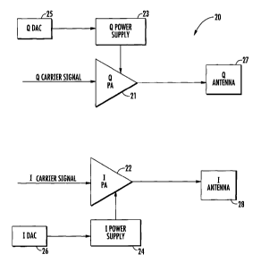
[0034] Referring now to FIG. 1, a communications device 20
according to the present disclosure is now described. The
communications device 20 illustratively includes an I power
amplifier 22 configured to generate an I amplified signal, a Q
power amplifier 21 configured to generate a Q amplified signal,
an I DAC 26 configured to generate an I signal, and a Q DAC
configured to generate a Q signal. The I and Q DACs 25-26 may
be operable using third or fourth generation cellular wireless
signals, for example, Long Term Evolution (LTE), Mobile WiMAX
(IEEE 802.16e-2005), etc. Of course, as will be appreciated by
those skilled in the art, other next generation signals may be
8
CA 02771480 2012-03-15
37035-CA-PAT
implemented in the communications device 20 with appropriate
modification.
[0035] The communications device 20 illustratively includes
an I power supply circuit 24 coupled to the I power amplifier 22
and to the I DAC 26 and configured to cause the I power
amplifier to modulate an I carrier signal into the I amplified
signal based upon the I signal. The communications device 20
illustratively includes a Q power supply circuit 23 coupled to
the Q power amplifier 21 and to the Q DAC 25 and configured to
cause the Q power amplifier to modulate a Q carrier signal into
the Q amplified signal based upon the Q signal. The I and Q
power supply circuits 23-24 effect the modulation by varying a
power supply voltage used by the I and Q power amplifiers 21-22.
[0036] Also, the communications device 20 illustratively
includes an I antenna 28 coupled to the I power amplifier 22,
and a Q antenna 27 coupled to the Q power amplifier 21. More
specifically, the I and Q antennas 28, 27 are illustratively
physically separated but adjacent to each other, for example,
spaced parallel to each other and at 100 m apart. The antennas
28, 27 are kept close together such that the radiation pattern
around them is as desired when the two operate simultaneously,
one radiating I path RF and the second radiating the Q path RF.
For example, the I and Q antennas 27-28 are illustratively
rectangular-shaped strip antennas that are adjacent to each
other. Of course, in other embodiments, the I and Q antennas
27-28 may have other shapes.
[0037] In other words, the combination of the amplified I and
Q signals occurs over-the-air and not upstream the antenna as in
typical communications devices. Advantageously, the combination
medium of air is quite favorable since it is a linear medium
with high dynamic range. Moreover, since the I and Q carrier
signals are constant envelop signals, the I and Q power
9
CA 02771480 2012-03-15
37035-CA-PAT
amplifiers 21-22 may operate in a saturated operation mode,
which is energy efficient, rather than the linear mode, as in
the typical communications device. Indeed, in the typical
communications device, a linear mode amplifier may be required
to successfully transmit the wideband third and fourth
generation wireless cellular signals. Unfortunately, this leads
to undesirably low battery life. In the disclosed
communications device 20, the battery life is advantageously
lengthened due to power amplifier efficiency.
[0038] Referring now to FIG. 2, the communications device 20
illustratively includes a transceiver integrated circuit (IC)
41. With the exception of the I and Q power supply circuits 23-
24, the I and Q power amplifiers 21-22, and the I and Q antennas
27-28, the transceiver IC 41 provides the processing resources
for all other components of the communications device 20.
[0039] The communications device 20 illustratively includes
an I LUT module 44 upstream of the I DAC 26 and configured to
supply a linear I signal thereto, and a Q LUT module 43 upstream
of the Q DAC 25 configured to supply a linear Q signal. The I
and Q LUT modules 43-44 ensure that the applied digital
modulation signal is represented linearly at the supply voltage
of the I and Q power amplifiers 21-22 as it goes through the I
and Q DACs 25-26, the reference input of the I and Q power
supply circuits 23-24 (which are illustratively shown as
switched mode power supplies DC-DC (SMPS)), and then to the
voltage supplied to the I and Q power amplifiers. As would be
appreciated by the skilled person, the output power versus
reference input voltage of the illustrated SMPS I and Q power
amplifiers 21-22 is not linear. Hence, the I and Q LUT modules
43-44 provide the necessary translation (look-up &
interpolation/ extrapolation) so that the output power is a
CA 02771480 2012-03-15
37035-CA-PAT
linear function of the DAC code applied at the input of the LUT
respective module.
[0040] Moreover, in some embodiments, envelope tracking of
the digital baseband I and Q signals may be implemented using
the I and Q power supply circuits 23-24. As will be appreciated
by the skilled person, the communications device 20 may include
a pair of duplexers (not shown) for providing a full duplex
transceiver.
(0041] The I and Q LUT modules 43-44 are used to linearize
the output power versus the digital baseband I and Q signals.
This is accomplished using calibration. In particular, the
digital baseband I signal is swept and the output power is
measured. The LUT entries are determined such that the transfer
characteristics of digital input to output power are linear.
[0042] Additionally, the communications device 20
illustratively includes a PLL 40 configured to generate the I
and Q carrier signals. The PLL 40 may be configured to generate
the I and Q carrier signals comprising constant envelop I and Q
carrier signals, for example. More specifically, the PLL 40
illustratively includes a phase frequency detector (PFD) 38, a
low pass filter 36 downstream therefrom, a signal generator 35
(e.g., a voltage controller oscillator (VCO)) downstream
therefrom, and a frequency divider 37 coupled between the signal
generator and the PFD.
[0043] Moreover, in the illustrated embodiment, the
communications device 20 illustratively includes an I pre-
amplifier 32 coupled upstream the I power amplifier 22, and a Q
pre-amplifier 31 coupled upstream the Q power amplifier 21. The
communications device 20 illustratively includes a 90-degree
phase shifter 33 coupled between the PLL 40 and the Q pre-
amplifier 31, and a 0 degrees phase shifter 34 coupled between
the PLL 40 and the I pre-amplifier 32. The communications
11
CA 02771480 2012-03-15
37035-CA-PAT
device 20 also illustratively includes a serial port module 30
coupled to the I power supply circuit 24. In the illustrated
SMPS embodiment, the serial port module 30 is used to control
the operating characteristics of the I and Q power supply
circuits 23-24 and to exercise programmability offered by the
SMPS, such as internal BW control etc. or switching between PWM
and PFM modes etc. as deemed appropriate by the software running
in the processor in the transceiver or the baseband processor.
[0044] Moreover, as will be appreciated by those skilled in
the art, the VCO (signal generator 35) may be operated at 2X or
even 4X the carrier frequency, and one or more frequency
dividers 37 may be used to divide the frequency to the specified
carrier frequency. This is done to help the transceiver IC 41
fight frequency pulling where the high output power at the I and
Q power amplifiers 21-22 centered as the carrier frequency
couples to the VCO and corrupts the phase noise.
[0045] An advantage of such frequency division is that all
four phases 0 , 90 , 180 and 270 of the RF carrier are readily
available. Since the power can only be positive, the I and Q
DACs 25-26 can only provide a positive signal to the I and Q
power supply circuits 23-24, which can only produce a voltage
between ground and VBATT. Hence, in contrast to a typical up-
conversion mixer that may allow positive and negative baseband
input voltage, this communications device 20 does not directly
allow negative inputs.
[0046] The way to accommodate the negative I DAC 26 input is
to choose 180 phase and to apply the inverted carrier to the I
power amplifier 22 input. Hence, positive I DAC values apply 0
phase to the I power amplifier 22 input, and negative I DAC
values apply 180 phase to the I power amplifier input.
Similarly, positive Q DAC values apply 90 phase to the Q power
amplifier 21 input, and negative Q DAC values apply 270 phase
12
CA 02771480 2012-03-15
37035-CA-PAT
to the Q power amplifier input. This is done by using the sign
bit to control a multiplexer (FIG. 15) that allows one or the
other phase of the carrier signal to the I and Q power amplifier
21-22 inputs. Hence, one multiplexer is needed for I path and
the second for Q path. The magnitudes of I DAC and Q DAC values
are always positive and, therefore, are applied to the
respective DACs 25-26.
[0047] In FIG. 2, it is assumed that the 0-degrees phase
shifter 34 provides,0 or 180 phase shifting based upon the
sign of the I DAC input to I power amplifier 22, and the 90-
degress phase shifter 33 provides 90 or 270 phase shifting
based upon the sign of Q DAC input to Q power amplifier 21. The
phase shifter 34 can be implemented using a multiplexer with
inputs 0 or 180 and the sign bit of I DAC input choosing 00
phase for positive inputs and 180 phase for negative inputs.
Similarly, the phase shifter 33 can be implemented using inputs
90 and 270 from the PLL 40 going into a second multiplexer
with 90 selected when Q DAC input is positive and 270 when it
is negative. Of course, this variation of the phase shifters
may also be applicable to the PLL circuits in other embodiments
disclosed herein.
[0048] In other embodiments, 2X or 4X rate VCO 35 outputs can
be divided to directly obtain the four needed phases. More
specifically, instead of generating the 90 /270 and 180 degree
phases, the VCO 35 in the PLL 40 may be designed at 2X or 4X or
even higher frequency and its output divided to obtain the
needed four phases 0 , 90 , 180 and 270 needed in accordance
with quadrature up-conversion. Phase 00 or 180 PLL outputs are
applied to the I power amplifier 22, and the sign of I signal
determines the selection between 00 and 180 .
[0049] Referring now to FIG. 3, another embodiment of the
communications device 20 is now described. In this embodiment
13
CA 02771480 2012-03-15
37035-CA-PAT
of the communications device 20', those elements already
discussed above with respect to FIGS. 1-2 are given prime
notation and most require no further discussion herein. This
embodiment differs from the previous embodiment in that the
communications device 20' exchanges the separate I and Q
antennas for a single antenna 28', and further includes a power
combiner 42' coupled between the antenna and the I and Q power
amplifiers 21'-22'. Moreover, this communications device 20'
illustratively includes I and Q controllers 45'-46' coupled
upstream of respective I and Q LUT modules 43'-44' for selecting
the desired phase shift for the respective phase shifters 33'-
34'.
[0050] Referring briefly and additionally to FIG. 15, another
embodiment of the communications device 20 is now described. In
this embodiment of the communications device 2011, those
elements already discussed above with respect to FIG. 3 are
given double prime notation and most require no further
discussion herein. This embodiment differs from the previous
embodiment in that the communications device 20'' includes a
pair of multiplexers 4711-481, coupled upstream of the I and Q
power amplifiers 2111-2211 for selectively providing the phase
shifted and I and Q signals, as discussed hereinabove.
[0051] Referring now to FIG. 4, another embodiment of a
communications device 50 is now described. This communications
device 50 illustratively includes a plurality of I power
amplifiers 52a-52b configured to respectively generate a
plurality of I amplified signals, a plurality of Q power
amplifiers 51a-51b configured to respectively generate a
plurality of Q amplified signals, a plurality of I antennas 54a-
54b respectively coupled to the plurality of I power amplifiers,
and a plurality of Q antennas 53a-53b respectively coupled to
the plurality of Q power amplifiers.
14
CA 02771480 2012-03-15
37035-CA-PAT
(0052] The communications device 50 illustratively includes
an I controller 56 coupled to the plurality of I power
amplifiers 52a-52b and configured to selectively enable at least
one of the plurality of I power amplifiers, and a Q controller
55 coupled to the plurality of Q power amplifiers 51a-51b and
configured to selectively enable at least one of the plurality
of Q power amplifiers. In particular, the I and Q controllers
55-56 enable as many power amplifiers 51a-52b as needed to
successfully transmit the signal. For example, fewer power
amplifiers 51a-52b would be enabled when the communications
device is near a network tower. Because of this selective
enabling of the power amplifiers 51a-52b, power-added efficiency
(PAE) versus power output is advantageously high. Those skilled
in art will appreciate that the communications device 50 acts as
an effective DAC that produces an electromagnetic output power
directly controlled by the I and Q controllers 55-56. This
effective DAC can also be called a digital-to-electromagnetic
converter (DEC).
[0053] Of course, as will be appreciated by the skilled
person, the illustrated embodiment includes two I and two Q
power amplifiers 51a-51b, but other embodiments may include
varying numbers, which may depend on the desired application.
For example, the communications device 50 may include 50 I power
amplifiers and 50 Q power amplifiers, each generating 20mW of
power for a total maximum potential power output of 2W.
Advantageously, since the power output of each power amplifier
4la-52b is reduced, the power amplifiers may be provided by a
single transceiver chip along with the other signal processing
elements, rather than being off-chip.
[0054] In another example, a 10-bit DEC can be designed by
placing 1024 pre-power amplifiers and associated antenna
segments. The digital control signal now directly selects the
CA 02771480 2012-03-15
37035-CA-PAT
output power produced. As described above, the sign bit of the
digital signal can be used to flip the carrier signal at the
= pre-power amplifiers inputs by 1800. The pre-power amplifier
segments can be constructed using similar techniques used to
build typical current source based DACs and using binary-to-
thermometer encoding to select the pre-power amplifiers. Those
skilled in the art can appreciate a wide range of typical DACs
that can directly be applied in this embodiment to DECs.
[0055] Referring now to FIG. 5, the communications device 50
illustratively includes an I DAC 58 configured to generate an I
bias current signal for the plurality of I power amplifiers 52a-
52c, and a Q DAC 57 configured to generate a Q bias current
signal for the plurality of Q power amplifiers 51a-51c. In
other words, the bias currents to the power amplifiers 51a-52c
are manipulated to effect the modulation of the I and Q carrier
signals.
[0056] Moreover, in the illustrated embodiment, the
communications device 50 includes an I LUT module 78 upstream of
the I DAC 58 and configured to supply a linear I signal thereto,
and a Q LUT module 79 upstream of the Q DAC 57 and configured to
supply a linear Q signal thereto. The I and Q LUT modules 78-79
are configured similarly to those of the embodiments of FIGS. 2-
3.
[0057] Additionally, the communications device 50
illustratively includes a PLL 70 configured to generate the I
and Q carrier signals. The PLL 70 may be configured to generate
the I and Q carrier signals comprising constant envelop I and Q
carrier signals, for example. More specifically, the PLL 70
illustratively includes a phase frequency detector (PFD) 71, a
low pass filter 72 downstream therefrom, a signal generator 73
downstream therefrom, and a frequency divider 74 coupled between
the signal generator and the PFD.
16
CA 02771480 2012-03-15
37035-CA-PAT
[0058] Moreover, in the illustrated embodiment, the
communications device 50 illustratively includes an I driver 64
coupled upstream the I power amplifiers 52a-52c, and a Q driver
63 coupled upstream the Q power amplifiers 5la-51c. The
communications device 50 illustratively includes a 90-degree
phase shifter 61 coupled between the PLL 70 and the Q driver 63,
and a 0 degrees phase shifter 62 coupled between the PLL 70 and
the I driver 64. As described above, the phase shifters 61-62
can be implemented by designing the VCO 73 at 2X or 4X RF
carrier frequency and dividing the frequency down to obtain the
carrier frequency. Using sign bit of DAC input and 2:1
multiplexer, these phase shifters 61-62 can be easily
implemented as described earlier. Also, the communications
device illustratively includes I and Q matching networks 66a-
66c, 65a-65c respectively coupled between the I and Q antennas
54a-54c, 53a-53c and the I and Q power amplifiers 52a-52c, 51a-
51c. The I and Q matching networks 66a-66c, 65a-65c may be
programmable and controlled digitally for antenna tuning, i.e.
varying voltage standing wave ratio (VSWR) at the antenna load.
[0059] Indeed, in some embodiments (not shown), the output of
the power amplifiers 51a-52b can be parasitically coupled, down-
converted and analog-to-digital (ADC) converted in the small
signal IC. Alternatively, a trace close to the antennas 53a-54c
can pick up the signal and feed it back into the small signal IC
where it is down-converted either using a receiver or a log-Amp
followed by an ADC. The tuning elements for matching can be
controlled to provide desirable tuning for output power under
varying VSWR at the antenna 53a-54c.
[0060] Referring now to FIG. 6, another embodiment of the
communications device 50 is now described. In this embodiment
of the communications device 50', those elements already
discussed above with respect to FIGS. 4-5 are given prime
17
CA 02771480 2012-03-15
37035-CA-PAT
notation and most require no further discussion herein. This
embodiment differs from the previous embodiment in that the
communications device 50' does not include the I and Q DACs and
= LUT modules. Rather, in this embodiment, the I and Q power
amplifiers 51a'-52c' are manipulated to modulate the I and Q
carrier signals via the I and Q controllers 55'-56'. In other
words, the I controller 56' is configured to cause the plurality
of I power amplifiers 52a'-52c' to modulate an I carrier signal
into the plurality of I amplified signals based upon an I
digital baseband signal, and the Q controller 55' is configured
to cause the plurality of Q power amplifiers 51a'-51c' to
modulate a Q carrier signal into the plurality of Q amplified
signals based upon a Q digital baseband signal. In particular,
the communications device 50' forms an effective DAC, and the
sign of the DAC input controls the appropriate phase carrier to
be selected, similar to as described for earlier embodiments.
The digital value is converted to magnitude and controls the
number of devices that are turned on. In this embodiment of a
DEC, the antenna segment is a part of the effective DAC.
[0061] Referring now to FIG. 7, another embodiment of a
communications device 80 is now described. This communications
device 80 illustratively includes a plurality of I power
amplifiers 84a-84b configured to respectively generate a
plurality of I amplified signals, a plurality of Q power
amplifiers 83a-83b configured to generate a plurality of Q
amplified signals, an I controller 82 coupled to the plurality
of I power amplifiers and configured to selectively enable at
least one of the plurality of I power amplifiers, and a Q
controller 81 coupled to the plurality of Q power amplifiers and
configured to selectively enable at least one of the plurality
of Q power amplifiers. This communications device 80
illustratively includes a power combiner 85 configured to
18
CA 02771480 2012-03-15
37035-CA-PAT
combine the plurality of I amplified signals and the plurality
of Q amplified signals in a combined amplified signal, and an
antenna 86 coupled to the power combiner.
[0062] Referring now to FIG. 8, the communications device 80
illustratively includes an I DAC 102 configured to generate an I
bias current signal for the plurality of I power amplifiers 84a-
84c, and a Q DAC 101 configured to generate a Q bias current
signal for the plurality of Q power amplifiers 83a-83c. In
other words, the bias currents to the power amplifiers 83a-84c
are manipulated to effect the modulation of the I and Q carrier
signals.
[0063] Moreover, in the illustrated embodiment, the
communications device 80 includes an I LUT module 104 upstream
of the I DAC 102 and configured to supply a linear I signal
thereto, and a Q LUT module 103 upstream of the Q DAC 101 and
configured to supply a linear Q signal thereto. The I and Q LUT
modules 103-104 are configured similarly to those of the
embodiments of FIGS. 2-3.
[0064] Additionally, the communications device 80
illustratively includes a PLL 93 configured to generate the I
and Q carrier signals. The PLL 93 may be configured to generate
the I and Q carrier signals comprising constant envelop I and Q
carrier signals, for example. More specifically, the PLL 93
illustratively includes a phase frequency detector (PFD) 94, a
low pass filter 95 downstream therefrom, a signal generator 97
downstream therefrom, and a frequency divider 96 coupled between
the signal generator and the PFD.
(0065] Moreover, in the illustrated embodiment, the
communications device 80 illustratively includes an I driver 88
coupled upstream the I power amplifiers 84a-84c, and a Q driver
87 coupled upstream the Q power amplifiers 83a-83c. The
communications device 80 illustratively includes a 90-degree
19
CA 02771480 2012-03-15
37035-CA-PAT
phase shifter 91 coupled between the PLL 93 and the Q driver 87,
and a 0 degrees phase shifter 92 coupled between the PLL 93 and
the I driver 88. Also, the communications device 80
illustratively includes I and Q capacitors 86a-86c, 85a-85c
respectively coupled between the power combiner 85 and the I and
Q power amplifiers 84a-84c, 83a-83c, each of the capacitors
being coupled to a ground potential. As described above, the
phase shifters 91-92 can be implemented by designing the VCO 97
at 2X or 4X RF carrier frequency and dividing the frequency down
to obtain the carrier frequency. Using sign bit of DAC input
and 2:1 multiplexer, these phase shifters 91-92 can be easily
implemented as described earlier.
[0066] Referring now to FIG. 9, another embodiment of the
communications device 80 is now described. In this embodiment
of the communications device 80', those elements already
discussed above with respect to FIGS. 7-8 are given prime
notation and most require no further discussion herein. This
embodiment differs from the previous embodiment in that the
communications device 80' does not include the I and Q DACs and
LUT modules. Rather, in this embodiment, the I and Q power
amplifiers 83a'-84c' are manipulated to modulate the I and Q
carrier signals via the I and Q controllers 81'-82'. In other
words, the I controller 82' is configured to cause the plurality
of I power amplifiers 84a'-84c' to modulate an I carrier signal
into the plurality of I amplified signals based upon an I
digital baseband signal, and the Q controller 81' is configured
to cause the plurality of Q power amplifiers 83a'-83c' to
modulate a Q carrier signal into the plurality of Q amplified
signals based upon a Q digital baseband signal.
[0067] The I and Q controllers 81'-82' operate similarly to
those of the embodiment described above in FIG. 6. This
embodiment here differs from the DEC described above in that
CA 02771480 2012-03-15
37035-CA-PAT
each DAC element now only drives a segment of the power combiner
85' and produces an RF output. Hence, it is more appropriately
an effective digital-to-RF (D-RF) converter.
[0068] Typical methods can be used to build the power
combiner 85', which can be implemented as a transformer with
many primaries and a single secondary that drives the antenna
86'. It is beneficial to combine the output power passively to
keep the output power combination very linear. Passive N:1
combiner structures can be employed; one D-RF converter element
drives one combiner element at its input. The D-RF converter
can be implemented using typical techniques used to build DACs,
such as arraying carefully to reduce the impact of INL and DNL,
binary to thermometer coding, shuffling the row-column decoders
of binary-to-thermometer encoder using barrel shifters to
implement dynamic element matching, employing dynamic weighted
averaging etc.
[0069] Referring now to FIGS. 10-13, a simulation of the
efficacy of the transmission characteristics of the
communications device 20 described in FIGS. 1-2 is now
described. Diagram 110 shows the combination of the amplified I
and Q signals over the air while chart 120 illustrates the I and
Q waveforms emitted by the I and Q antennas 27-28. The chart
120 shows that one wave travels slightly more than the other
with the distance shown as. I12 -11 1 .
[0070] With reference to diagram 130, the formula:
112 -111= kI(r cos(q$) + d / 2)2 + r2 sin2 (q$) - (r cos(q) - d / 2)2 + r2
sin2 (b)+
is illustrated. If r=kd, the formula resolves to:
I r2+d2/4-rdcos(q$)I
21
CA 02771480 2012-03-15
37035-CA-PAT
[0071] The plot of 112-1,1 is shown in diagram 140 of FIG. 13.
At 2 GHz and 150mm away from the antenna, the experienced IQ
imbalance is 2.4*d degrees, where d is measured in mm. The IQ
imbalance due to separate antennas can be made less than the IQ
imbalance floor of the transmitter by keeping the two antennas
very close, thereby enabling successful receipt of the over-the-
air combined I and Q signal.
[0072] Example components of a mobile wireless communications
device 1000 that may be used in accordance with the above-
described embodiments are further described below with reference
to FIG. 14. The device 1000 illustratively includes a housing
1200, a keyboard or keypad 1400 and an output device 1600. The
output device shown is a display 1600, which may comprise a full
graphic liquid crystal display (LCD). Other types of output
devices may alternatively be utilized. A processing device 1800
is contained within the housing 1200 and is coupled between the
keypad 1400 and the display 1600. The processing device 1800
controls the operation of the display 1600, as well as the
overall operation of the mobile device 1000, in response to
actuation of keys on the keypad 1400.
[0073] The housing 1200 may be elongated vertically, or may
take on other sizes and shapes (including clamshell housing
structures). The keypad may include a mode selection key, or
other hardware or software for switching between text entry and
telephony entry.
[0074] In addition to the processing device 1800, other parts
of the mobile device 1000 are shown schematically in FIG. 14.
These include a communications subsystem 1001; a short-range
communications subsystem 1020; the keypad 1400 and the display
1600, along with other input/output devices 1060, 1080, 1100 and
1120; as well as memory devices 1160, 1180 and various other
22
CA 02771480 2012-03-15
37035-CA-PAT
device subsystems 1201. The mobile device 1000 may comprise a
two-way RF communications device having data and, optionally,
voice communications capabilities. In addition, the mobile
device 1000 may have the capability to communicate with other
computer systems via the Internet.
[0075] Operating system software executed by the processing
device 1800 is stored in a persistent store, such as the flash
memory 1160, but may be stored in other types of memory devices,
such as a read only memory (ROM) or similar storage element. In
addition, system software, specific device applications, or
parts thereof, may be temporarily loaded into a volatile store,
such as the random access memory (RAM) 1180. Communications
signals received by the mobile device may also be stored in the
RAM 1180.
[0076] The processing device 1800, in addition to its
operating system functions, enables execution of software
applications 1300A-1300N on the device 1000. A predetermined
set of applications that control basic device operations, such
as data and voice communications 1300A and 1300B, may be
installed on the device 1000 during manufacture. In addition, a
personal information manager (PIM) application may be installed
during manufacture. The PIM may be capable of organizing and
managing data items, such as e-mail, calendar events, voice
mails, appointments, and task items. The PIM application may
also be capable of sending and receiving data items via a
wireless network 1401. The PIM data items may be seamlessly
integrated, synchronized and updated via the wireless network
1401 with corresponding data items stored or associated with a
host computer system.
[0077] Communication functions, including data and voice
communications, are performed through the communications
subsystem 1001, and possibly through the short-range
23
CA 02771480 2012-03-15
37035-CA-PAT
communications subsystem 1020. The communications subsystem
1001 includes a receiver 1500, a transmitter 1520, and one or
more antennas 1540 and 1560. In addition, the communications
subsystem 1001 also includes a processing module, such as a
digital signal processor (DSP) 1580, and local oscillators (LOs)
1601. The specific design and implementation of the
communications subsystem 1001 is dependent upon the
communications network in which the mobile device 1000 is
intended to operate. For example, a mobile device 1000 may
include a communications subsystem 1001 designed to operate with
the MobitexTM, Data TACTM or General Packet Radio Service (GPRS)
mobile data communications networks, and also designed to
operate with any of a variety of voice communications networks,
such as Advanced Mobile Phone System (AMPS), time division
multiple access (TDMA), code division multiple access (CDMA),
Wideband code division multiple access (W-CDMA), personal
communications service (PCS), GSM (Global System for Mobile
Communications), enhanced data rates for GSM evolution (EDGE),
etc. Other types of data and voice networks, both separate and
integrated, may also be utilized with the mobile device 1000.
The mobile device 1000 may also be compliant with other
communications standards such as 3GSM, 3rd Generation
Partnership Project (3GPP), Universal Mobile Telecommunications
System (UMTS), 4G, etc.
[0078] Network access requirements vary depending upon the
type of communication system. For example, in the Mobitex and
DataTAC networks, mobile devices are registered on the network
using a unique personal identification number or PIN associated
with each device. In GPRS networks, however, network access is
associated with a subscriber or user of a device. A GPRS device
therefore typically involves use of a subscriber identity
24
CA 02771480 2012-03-15
37035-CA-PAT
module, commonly referred to as a SIM card, in order to operate
on a GPRS network.
[0079] When required network registration or activation
procedures have been completed, the mobile device 1000 may send
and receive communications signals over the communication
network 1401. Signals received from the communications network
1401 by the antenna 1540 are routed to the receiver 1500, which
provides for signal amplification, frequency down conversion,
filtering, channel selection, etc., and may also provide analog
to digital conversion. Analog-to-digital conversion of the
received signal allows the DSP 1580 to perform more complex
communications functions, such as demodulation and decoding. In
a similar manner, signals to be transmitted to the network 1401
are processed (e.g. modulated and encoded) by the DSP 1580 and
are then provided to the transmitter 1520 for digital to analog
conversion, frequency up conversion, filtering, amplification
and transmission to the communication network 1401 (or networks)
via the antenna 1560.
[0080] In addition to processing communications signals, the
DSP 1580 provides for control of the receiver 1500 and the
transmitter 1520. For example, gains applied to communications
signals in the receiver 1500 and transmitter 1520 may be
adaptively controlled through automatic gain control algorithms
implemented in the DSP 1580.
[0081] In a data communications mode, a received signal, such
as a text message or web page download, is processed by the
communications subsystem 1001 and is input to the processing
device 1800. The received signal is then further processed by
the processing device 1800 for an output to the display 1600, or
alternatively to some other auxiliary I/O device 1060. A device
may also be used to compose data items, such as e-mail messages,
using the keypad 1400 and/or some other auxiliary I/O device
CA 02771480 2012-03-15
37035-CA-PAT
1060, such as a touchpad, a rocker switch, a thumb-wheel, or
some other type of input device. The composed data items may
then be transmitted over the communications network 1401 via the
communications subsystem 1001.
[0082] In a voice communications mode, overall operation of
the device is substantially similar to the data communications
mode, except that received signals are output to a speaker 1100,
and signals for transmission are generated by a microphone 1120.
Alternative voice or audio I/O subsystems, such as a voice
message recording subsystem, may also be implemented on the
device 1000. In addition, the display 1600 may also be utilized
in voice communications mode, for example to display the
identity of a calling party, the duration of a voice call, or
other voice call related information.
[0083] The short-range communications subsystem enables
communication between the mobile device 1000 and other proximate
systems or devices, which need not necessarily be similar
devices. For example, the short-range communications subsystem
may include an infrared device and associated circuits and
components, a BluetoothTM communications module to provide for
communication with similarly-enabled systems and devices, or a
NFC sensor for communicating with a NFC device or NFC tag via
NFC communications.
[0084] Many modifications and other embodiments will come to
the mind of one skilled in the art having the benefit of the
teachings presented in the foregoing descriptions and the
associated drawings. Therefore, it is understood that various
modifications and embodiments are intended to be included within
the scope of the appended claims.
26