Note: Descriptions are shown in the official language in which they were submitted.
CA 02771757 2012-02-21
WO 2010/095084 PCT/IB2010/050663
1
DIMMABLE LIGHT SOURCE WITH SHIFT IN COLOUR TEMPERATURE
FIELD OF THE INVENTION
The present invention relates in general to an illumination device comprising
LEDs as light sources.
BACKGROUND OF THE INVENTION
The use of LEDs as light source for illumination rather than mere indicator
lights is well known, since the development of high-power LEDs. It is also
rather standard
that an illumination device is powered from mains, typically 230 V @ 50 Hz in
Europe.
Since LEDs require a relatively low voltage (typically in the order of 3 V)
and allow current
flow in one direction only, driver circuits have been developed for generating
a DC LED
current on the basis of the AC mains. However, such driver circuits are
relatively expensive.
In a more simple approach, a string of LEDs is connected to mains directly, in
series with a ballast resistor. For allowing LED current and thus light output
in both halves of
the AC period, two such strings are connected anti-parallel. The idea would be
that, for
instance, 70 LEDs would accommodate a voltage drop of 210 V, while the
remaining 20 V
would be accommodated by the ballast resistor. Voltage variations would be
taken up by the
ballast resistor.
Although the simplicity of this approach, and hence the relatively cheap
implementation thereof, has a certain attractiveness, there is a problem when
it is desired that
the illumination device is dimmed.
For certain applications, it is not only desired that the illumination device
is
dimmable, but also that the colour temperature of the output light is shifted
to a lower value
on dimming. This requirement is specifically important in the case of small
bedside lamps or
reading lamps, but it may be that there are other applications where the same
feature would
be desirable.
SUMMARY OF THE INVENTION
An object of the present invention is to provide a simple and cost-efficient
illumination device having a plurality of LEDs as light sources, capable of
being dimmed in a
CA 02771757 2012-02-21
WO 2010/095084 PCT/IB2010/050663
2
simple manner while simultaneously the light output of the device shifts to a
lower colour
temperature automatically.
According to an important aspect of the present invention, a tunable voltage
source is connected in series with at least one white LED, this voltage source
powering at
least one red LED. When the output power of the voltage source is increased,
the voltage
drop over the voltage source is increased so that the white LED receives less
power while the
red LED receives more power.
Further advantageous elaborations are mentioned in the dependent claims.
BRIEF DESCRIPTION OF THE DRAWINGS
These and other aspects, features and advantages of the present invention will
be further explained by the following description of one or more preferred
embodiments with
reference to the drawings, in which same reference numerals indicate same or
similar parts,
and in which:
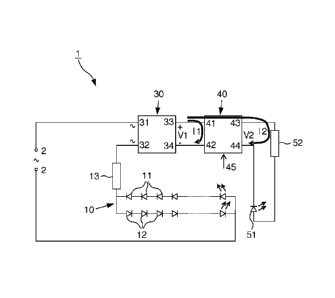
figure 1 schematically shows a block diagram of an illumination device;
figure 2 schematically shows a block diagram of a voltage source for use in
the illumination
device of figure 1.
DETAILED DESCRIPTION OF THE INVENTION
Figure 1 schematically shows a block diagram of an illumination device 1
according to the present invention. The illumination device 1 comprises input
terminals 2 for
coupling to AC mains. A LED string 10 is connected in series with the input
terminals 2. The
LED string 10 comprises a first series of primary power LEDs 11 and a second
series of
primary power LEDs 12 connected anti-parallel to the first series. A first
ballast resistor 13 is
connected in series with the LED string 10.
The primary LEDs 11, 12 are preferably white LEDs. However, it is also
possible that one or more of these LEDs are coloured LEDs.
A rectifier 30 has its input terminals 31, 32 mounted in series with the LED
string 10. The rectifier 30 may suitably comprise a bridge circuit of diodes,
as commonly
known.
At its output terminals 33, 34, the rectifier 30 provides a rectified DC
voltage
VI. If required, this voltage may be smoothed by a capacitor in parallel to
the output
terminals 33, 34, but this is not shown for sake of simplicity.
CA 02771757 2012-02-21
WO 2010/095084 PCT/IB2010/050663
3
The illumination device 1 further comprises a controllable voltage source 40,
having input terminals 41, 42 coupled to the rectifier output terminals 33, 34
to receive the
rectified DC voltage V1 as input voltage. Reference numeral 45 indicates a
user-controllable
control input. At its output terminals 43, 44, the controllable voltage source
40 provides a DC
output voltage V2, of which the magnitude depends on the input received at the
user control
input 45. A series arrangement of at least one auxiliary LED 51 and a second
ballast resistor
52 is connected to the output terminals 43, 44 of the controllable voltage
source 40.
Normally, only one auxiliary LED 51 will be sufficient, but the gist of the
present invention is also applicable if two or more auxiliary LEDs are
connected in series.
Preferably, the auxiliary LED 51 is a red power LED. However, the gist of the
present invention is also applicable if the colour of the auxiliary LED 51 has
a lower colour
temperature than the colour of the primary power LEDs 11, 12. For instance, an
embodiment
would be possible where the primary power LEDs 11, 12 are white LEDs while the
auxiliary
LED 51 is an orange or yellow LED. Further, in the case of multiple auxiliary
LEDs, it is not
essential that all auxiliary LEDs mutually have the same colour.
It is noted that, in stead of a controllable voltage source 40, a controllable
current source can be used.
It is further noted that, in stead of a controllable DC voltage (or current)
source, a controllable AC voltage (or current) source can be used. In that
case, the rectifier 30
can be omitted, and the auxiliary LEDs may comprise at least two LEDs mounted
anti-
parallel.
The primary LEDs 11, 12 and the auxiliary LED(s) 51 are mounted close
together in the illumination device 1, so that the overall output light as
produced by the
illumination device 1 as a whole, as perceived by a user, is a mixture of the
individual light
outputs of the individual LEDs 11, 12, 51.
The current provided by the mains and received by the LED string 10 will be
indicated as Imains. This current is also received as input current by the
rectifier 30. It is
assumed that no current is lost in the rectifier 30. The rectified mains
current (output current
of the rectifier 30), which will be indicated as <Imains>, is provided as
input current to the
voltage source 40. Part of the rectified mains current will be consumed by the
controllable
voltage source 40: this current will be indicated as ballast current 11. The
current produced at
the output of the voltage source 40 and received by the auxiliary LED 51 will
be indicated as
auxiliary current 12. Thus, it should be clear that <Imains> = 11 + 12.
CA 02771757 2012-02-21
WO 2010/095084 PCT/IB2010/050663
4
The operation is as follows. Assume that the user has set the controllable DC
voltage source 40 to a low output voltage, so that the auxiliary LED 51 does
produce no light
or only a small amount of light. Then, the voltage drop over the input
terminals 41, 42 of the
voltage source 40 is relatively low, and consequently the voltage drop over
the input
terminals 31, 32 of the rectifier 30 is low, so the LED string 10 receives the
maximum drive
voltage and produces maximum light output.
Assume that the user is adjusting the controllable DC voltage source 40 to a
higher output voltage. As a consequence, the auxiliary LED 51 produces an
increased amount
of light. Simultaneously, the voltage drop over the input terminals 41, 42 of
the voltage
source 40 is increasing and hence the voltage drop over the input terminals
31, 32 of the
rectifier 30 is increasing, the drive voltage for the LED string 10 is
decreasing and the
amount of light produced by the LED string 10 is decreasing. All in all, the
light output level
of the illumination device is reduced (dimmed), while the relative content of
red light in the
output light is increased (shift to lower colour temperature).
Figure 2 is a block diagram of an embodiment of the voltage source 40 which
is preferred because of its simplicity. A tuneable Zener diode 49 (for
instance the standard
component TL431 or LM43 1, commercially available from, for instance,
Motorola, Texas
Instruments, Fairchild Semiconductor) is connected in parallel to the output
terminals 43, 44.
A series arrangement of a first resistor 46 and a second resistor 47 is
connected in parallel to
the input terminals 41, 42. The node between the two resistors 46, 47 is
connected to a
control input terminal 48 of the tuneable Zener diode 49. The positive output
terminal 43 is
connected to the positive input terminal 41, and the negative output terminal
44 is connected
to the negative input terminal 42. One of the said resistors 46, 47 is an
adjustable resistor and
implements the user control input 45; in the embodiment as shown, this applies
to the first
resistor 46 connected to the positive input terminal 41.
With the circuit of figure 2, the output voltage V2 meets the formula
V2 = (1 + Rl/R2)=Vref, wherein
RI is the resistance value of the first resistor 46;
R2 is the resistance value of the second resistor 47;
Vref is an internal reference voltage of the tuneable Zener diode 49,
typically
about 1.2 V or 2.5 V.
It is noted that in this circuit V 1 = V2.
If RI = 0, the output voltage V2 will be equal to Vref, too low for the
auxiliary
LED 51 to draw a current (depending on the properties of the auxiliary LED 51
and second
CA 02771757 2012-02-21
WO 2010/095084 PCT/IB2010/050663
ballast resistor 52). Since also the input voltage VI will be equal to Vref,
the LED string 10
receives almost the full mains voltage. The resulting large main current
<Imains> will flow
mainly through the Zener 49 and partly through the second resistor 47.
If RI is increased, the output voltage V2 will increase, so that the auxiliary
5 LED 51 can draw more current 12 (the precise amount of auxiliary current 12
will depend on
the properties of the auxiliary LED 51 and second ballast resistor 52). Since
also the input
voltage V1 increases, the LED string 10 receives less voltage and will thus
draw less main
current Imain. The difference 11 = <Imains> - 12 will flow mainly through the
Zener 49,
indicated as Iz, and partly through the first and second resistors 46, 47. As
should be clear to
a person skilled in the art, a proper dimensioning of the components,
particularly the first and
second ballast resistors 13, 52 and the forward voltages of the LEDs 11, 12,
51, in
conjunction with the number of LEDs and their light output, will result in the
desired colour
shift while dimming.
Summarizing, the present invention provides an illumination device 1
comprising:
- input terminals 2 for coupling to AC mains;
- a LED string 10 connected in series with the input terminals;
- a rectifier 30, having input terminals connected in series with the LED
string;
- a controllable voltage source 40, having input terminals coupled to the
rectifier output terminals;
- a series arrangement of at least one auxiliary LED 51 and a second ballast
resistor 52 connected to the output terminals of the controllable voltage
source.
The voltage source comprises:
a series arrangement of an adjustable first resistor 46 and a second resistor
47
connected in parallel to the input terminals;
a tuneable Zener diode 49 connected in parallel to the output terminals,
having a
control input terminal 48 connected to the node between the two resistors.
The positive output terminal is connected to the positive input terminal and
the
negative output terminal is connected to the negative input terminal.
While the invention has been illustrated and described in detail in the
drawings
and foregoing description, it should be clear to a person skilled in the art
that such illustration
and description are to be considered illustrative or exemplary and not
restrictive. The
invention is not limited to the disclosed embodiments; rather, several
variations and
modifications are possible within the protective scope of the invention as
defined in the
CA 02771757 2012-02-21
WO 2010/095084 PCT/IB2010/050663
6
appending claims. For instance, the first ballast resistor 13 may be displaced
toward the
rectifier 30 or the source 40.
Further, the LED string 10 may have a configuration differing from the
configuration shown in figure 1. For example, the LED string may be
implemented as a
series arrangement of LED units, wherein each LED unit comprises at least one
first LED
connected anti-parallel to at least one second LED. Other ladder
configurations are
conceivable, too.
Other variations to the disclosed embodiments can be understood and effected
by those skilled in the art in practicing the claimed invention, from a study
of the drawings,
the disclosure, and the appended claims. In the claims, the word "comprising"
does not
exclude other elements or steps, and the indefinite article "a" or "an" does
not exclude a
plurality. A single processor or other unit may fulfill the functions of
several items recited in
the claims. The mere fact that certain measures are recited in mutually
different dependent
claims does not indicate that a combination of these measures cannot be used
to advantage. A
computer program may be stored/distributed on a suitable medium, such as an
optical storage
medium or a solid-state medium supplied together with or as part of other
hardware, but may
also be distributed in other forms, such as via the Internet or other wired or
wireless
telecommunication systems. Any reference signs in the claims should not be
construed as
limiting the scope.