Note: Descriptions are shown in the official language in which they were submitted.
CA 02771958 2012-03-09
UNIFIED FREQUENCY SYNTHESIZER FOR DIRECT CONVERSION
RECEIVER OR TRANSMITTER
Statement of the Technical Field
[00011 The inventive arrangements relate to methods and systems for
communication devices, and more particularly to systems and methods for
frequency
conversion in radio frequency communication devices.
Description of the Related Art
[00021 Frequency synthesizers are commonly used to generate local oscillator
signals used in radio frequency conversion operations. For example, these
signals can
be used in mixers to perform up-conversion and down-conversion of signals. In
portable radios, the frequency synthesizer section of the Radio Frequency (RF)
module is often the largest and the most expensive portion of the design.
Multiband
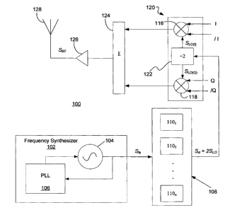
frequency synthesizers for radios that operate on multiple bands are often
larger and
more complex than synthesizers for band specific radios. One option to support
multiband transceiver functionality is to use a frequency synthesizer that can
tune
over a very broad range of frequencies sufficient cover all of the bands. This
approach has the advantage of requiring only one synthesizer, but such designs
are
necessarily more complex. For example, they often require offset loops, broad
band
networks, high tuning voltages and so on. Moreover, the performance of a very
broad
tuning synthesizers are generally inferior to synthesizers that tune over a
more narrow
range.
[00031 An alternative approach to a single synthesizer that tunes over a very
broad
range of frequencies involves use of multiple synthesizers, each capable of
tuning
over a relatively narrow band of frequencies. The advantage of the multiple
frequency synthesizer approach is that performance is not compromised in the
way
that it is with very broad tuning synthesizers. However, these multiple
frequency
synthesizer designs tend to be expensive, as each additional frequency
synthesizer
adds cost to the system. Use of multiple frequency synthesizers typically also
involves more research and development effort and added time to market, since
frequency synthesizers tend to be complex designs. Another problem with the
-1-
CA 02771958 2012-03-09
multiple synthesizer approach is that more space is needed to fit the
additional
synthesizer units. This can be a significant issue in a portable radio design.
Finally,
the multiple synthesizer approach usually requires the addition of a band
switching
network to route the synthesized RF signal for the various RF frequency bands
to the
appropriate frequency conversion circuitry.
SUMMARY OF THE INVENTION
[0004] The invention concerns a method and system for providing a single RF
synthesizer with a strategically selected tune range and a divider network to
permit
direct conversion coverage of all of the relevant bands of a land mobile radio
(LMR)
or other types of radio. The method involves generating a first signal Sfs
using a
frequency synthesizer having a predetermined synthesizer tuning range. A
second
signal Sd is generated which can have any one of a several different
predetermined
second tuning ranges. The second signal is generated by selectively performing
a
frequency dividing operation on the first signal in accordance with any one of
a
plurality of predetermined integer divisor values. The second signal is then
used in a
modulator or demodulator to perform a frequency conversion operation on a
third
signal. The frequency conversion can include a direct conversion from a
frequency of
a received or transmitted RF signal, to or from a baseband signal. In some
embodiments, the frequency conversion includes quadrature modulation or
quadrature
demodulation of a signal.
[0005] The invention also concerns a communication device which includes a
frequency synthesizer. The frequency synthesizer generates a first signal Sf,
within a
predetermined synthesizer tuning range of the frequency synthesizer. A divider
module is provided to selectively generate a second signal Sd having any one
of a
plurality of predetermined second tuning ranges. The divider module is
configured to
generate the second tuning ranges by selectively performing a frequency
dividing
operation on the first signal in accordance with any one of a plurality of
predetermined divisor values. A frequency conversion device is included in the
communication device. The frequency conversion device can include a modulator
or
-2-
CA 02771958 2012-03-09
demodulator and is configured to use the second signal to perform a frequency
conversion operation on a third signal. In some embodiments, the frequency
conversion device is configured to directly convert a frequency of a received
or
transmitted RF signal, to or from a baseband signal. The frequency conversion
device
can be a quadrature modulator or quadrature demodulator.
[00061 According to yet another aspect, the invention concerns a direct
conversion communication device. The device includes a single frequency
synthesizer generating a frequency synthesizer output signal. At least one
frequency
divider is provided for generating a reduced frequency signal by selectively
dividing
the single frequency synthesizer output signal by an integer divisor value.
Significantly, the device is configured to vary the reduced frequency signal
so as to
include every frequency the direct conversion communication device is designed
to
receive within a plurality of frequency bands. This is accomplished in the
device by
adjusting a frequency of the single synthesizer output signal and the divisor
value.
BRIEF DESCRIPTION OF THE DRAWINGS
100071 Embodiments will be described with reference to the following drawing
figures, in which like numerals represent like items throughout the figures,
and in
which:
[00081 FIG. 1 is a block diagram of a transmitter which is useful for
understanding the present invention.
[00091 FIG. 2 is a block diagram of a receiver that is useful for
understanding the
present invention.
[00101 FIG. 3 is a block diagram of a transceiver that is useful for
understanding
the present invention.
[0011] FIG. 4 is a table of synthesizer calculations that is useful for
understanding
the present invention.
[00121 FIG. 5 is a table showing LMR and military band coverage with a 1516
MHz to 2088 MHz VCO.
-3-
CA 02771958 2012-03-09
[00131 FIG. 6 is a table showing RF frequency coverage with a 512 MHz to 1024
MHz VCO.
[00141 FIG. 7 is a table showing RF frequency coverage with a 1920 MHz to
4000 MHz VCO.
DETAILED DESCRIPTION
[00151 The present invention is described with reference to the attached
figures,
wherein like reference numbers are used throughout the figures to designate
similar or
equivalent elements. The figures are not drawn to scale and they are provided
merely
to illustrate the present invention. Several aspects of the invention are
described
below with reference to example applications for illustration. It should be
understood
that numerous specific details, relationships, and methods are set forth to
provide a
full understanding of the invention. One having ordinary skill(s) in the
relevant art,
however, will readily recognize that the invention can be practiced without
one or
more of the specific details or with other methods. In other instances, well-
known
structures or operation are not shown in detail to avoid obscuring the
invention. The
present invention is not limited by the illustrated ordering of acts or
events, as some
acts may occur in different orders and/or concurrently with other acts or
events.
Furthermore, not all illustrated acts or events are required to implement a
methodology in accordance with the present invention.
[00161 The invention concerns a method and system by which an RF synthesizer
with a selected tune range facilitates direct conversion coverage of all of
the relevant
bands of a radio device. Modern LMR radios are expected to provide direct
conversion coverage for the several bands of frequencies including (1) VHF
band:
136-174 MHz, (2) the 220 MHz band: 220-222 MHz, (3) UHF band: 380-520 MHz,
(4) 700/800 MHz band: 762-870 MHz, hereinafter "the LMR bands." Radios used by
the military can include these as well as other bands. The output of an RF
synthesizer
is coupled to a divider network that allows the limited frequency range output
of the
synthesizer to be converted to the tuning ranges that are necessary for direct
conversion of all of the LMR or military bands. A single RF synthesizer can
therefore
-4-
CA 02771958 2012-03-09
be used to facilitate transmit and receive processing of all such bands.
Advantageously, only a single phase locked loop is required for the design,
and the
loop runs at the tune frequency, not the output frequency. The dividers used
in the
present invention can be implemented as hardware or software.
[00171 Referring now to FIG. 1, there is shown a direct conversion type
transmitter circuit 100 which includes a frequency synthesizer 102, a divider
module
108, a modulator 120, and a summer 124. In RF communication systems, a direct
conversion transmitter is one in which a baseband modulation signal is
directly
converted to a frequency of a desired transmitter RF output carrier signal.
This
generally requires that a signal used for RF mixing (sometimes called a local
oscillator signal) is synchronized in frequency to the desired transmitter RF
output
carrier signal. An advantage of the direct conversion transmitter is that it
requires
only one stage of up-conversion or mixing. The direct conversion approach also
reduces the number of filters that are required.
[0018] In the direct conversion transmitter in FIG. 1, the frequency
synthesizer
102 generates a an RF signal which can be varied over a range of frequencies.
The
output of the frequency synthesizer is communicated to the divider module 108
which
reduces the frequency of the RF signal in accordance with some integer divisor
value.
For example, if a divisor value of two is selected, the divider module will
provide an
output frequency which is half the RF frequency of the frequency synthesizer
102.
The output of the divider module 108 is communicated to the modulator 120.
[00191 The modulator will typically perform two functions. It will modulate
the
RF carrier signal from the divider module in accordance with some
predetermined
transmitter modulation format and will convert an input signal at baseband
frequency,
to a transmitter carrier frequency. In the embodiment shown, an I/Q modulator
is
used for this purpose. The I/Q input values comprise a baseband signal which
is
converted directly to a transmitter carrier frequency by the modulator 120.
The
modulator performs a frequency conversion on the baseband signal to produce in-
phase and quadrature-phase signals at the carrier frequency. These in-phase
and
quadrature phase signals are combined in the summer 124 to generate a low
power
-5-
CA 02771958 2012-03-09
transmit signal at the carrier frequency. A power level of this low-power
transmit
signal is increased in an amplifier 126 to produce a high power transmit
signal, which
is then communicated to an antenna 128. Notably, the direct conversion
transmitter
can have more or fewer components than those illustrated in FIG. 1. However,
the
components shown are sufficient to disclose an illustrative embodiment
implementing
the present invention.
[00201 Frequency synthesizers are well known in the art and frequency
synthesizer 102 will not be described here in detail so as to avoid obscuring
the
invention. In general, however, the frequency synthesizer 102 will include a
phase
locked loop (PLL) 106 and a voltage controlled oscillator (VCO) 104. The
frequency
synthesizer 102 can produce a particular output frequency within a
predetermined
tuning frequency range in response to one or more control signal inputs (not
shown).
Advantageously, unlike the operation of multiple VCOs to implement multiple
bands
of operation, only a single phase locked loop is required for the design. The
loop runs
at the tune frequency of the single VCO, while the output local oscillator
signal can be
changed based on the selected divide ratio. In some embodiments, the PLL 106
can
be an integer-N type PLL. Alternatively, if reduced phase noise is desired, a
fractional-N type PLL device can be advantageously used instead. Still, it
should be
understood that any suitable frequency synthesizer design can be used for the
present
invention, provided that the frequency synthesizer is capable of producing a
synthesized output frequency in the necessary ranges described below. For
convenience, the output of the frequency synthesizer shall be referred to
herein as Sfs.
(00211 The output of the frequency synthesizer is communicated to a divider
module 108. The divider module 108 provides a plurality of frequency dividers
1101,
1102, ... 110,, which are capable of accepting an input signal of frequency fõ
and
generating an output frequency foõ 1 = f/n where the divisor n is an integer.
Frequency
dividers are well known in the art. Accordingly, frequency dividers 1101,
1102, .. .
110õ will not be described in detail in order to avoid obscuring the
invention.
However, it should be understood that any type of frequency divider can be
used with
the present invention provided that it is capable of performing frequency
division as
-6-
CA 02771958 2012-03-09
described herein. Frequency dividers used with the present invention can be
analog or
digital devices. For example, the frequency divider can be regenerative
frequency
divider, an injection-locked frequency divider, or a digital frequency
divider. The
frequency dividers can be implemented in hardware, software, or a combination
of
hardware and software. In some instances, one or more frequency dividers 1101,
1102, ... 110õ can be implemented as a single frequency divider that is
selectively
configurable to perform frequency dividing operations for several different
value of n.
Alternatively, a plurality of frequency dividers can be used for this purpose,
in which
case suitable switching circuitry can be provided in divider module 108 to
selectively
route signals to and from each divider. For convenience, the signal output
from the
divider module shall be referred to herein as Sd.
[00221 The output of the divider module Sd is communicated to I/Q modulator
120. A modulator is a device which accepts a baseband input signal and outputs
a
radio frequency (RF) modulated signal. As used herein, the term baseband
refers to a
signal that includes frequencies that range from very close to zero (0) hertz
to some
cut-of frequency, which usually is a maximum bandwidth of a signal. Baseband
signals are often used to modulate a higher frequency carrier wave in order
that it may
be transmitted by radio. The low frequency components comprising the baseband
signal are used in such instances to modulate the higher frequency carrier
wave signal
(an RF signal) in accordance with a modulation scheme. Alternatively, a
baseband
signal can be extracted from a higher frequency signal (an RF signal) using a
demodulator.
[00231 In the present invention, the modulator 120 can be any suitable type of
modulator device. However, according to some embodiments, the modulator 120
can
be an I/Q type modulator which facilitates quadrature amplitude modulation
(QAM)
methods. If the modulator 120 is an I/Q type modulator, it will generally
include a
phase splitter 122. In some embodiments, the phase splitter 122 can be a
polyphase
filter that generates the quadrature signals used to drive a pair of mixers
116, 118,
which are also sometimes referred to as multipliers. However, polyphase
filters have
a limited bandwidth and it can therefore be advantageous to instead use a
digital
-7-
CA 02771958 2012-03-09
circuit to implement a broadband phase splitter. Such digital circuits used to
implement broadband phase splitters are well known in the art and therefore
will not
be described here in detail. However, they essentially consist of D-type flip-
flops and
an inverter which are configured to produce precise quadrature outputs.
100241 While digital circuits used to implement broadband phase splitters can
advantageously permit excellent quadrature signal generation over a multi-
octave
frequency range, they do require an input frequency which is twice the desired
local
oscillator frequency (commonly referred to as 2*LO). FIG. 1 shows an
embodiment
of the invention that uses a 2*LO input to produce a desired local oscillator
signal
SLO(q, SLO(Q) that has the desired local oscillator frequency. Still, it
should be
appreciated that the invention is not limited in this regard and other types
of phase
splitters can also be used with the present invention.
[00251 Of course, if the phase splitter selected does not require 2*LO as an
input,
then the frequency of Sfs and/or Sd must be adjusted as necessary to produce a
desired
local oscillator frequency. More particularly, if the quadrature LO generation
method
does not involve a phase splitter that incorporates a frequency divide-by-2
element,
the divide ratios chosen to implement a particular frequency plan would shift
lower by
a factor of two so as to result in the appropriate LO frequency for the
conversion.
Similarly, the frequency of the 2*LO tune range can be increased with a
corresponding increase in the required divide ratios, such as doubling the
2*LO
frequency, yielding 4*LO, and correspondingly increasing the divide ratios by
a
factor of two so as to obtain the same desired tune ranges.
[00261 Within the modulator 120, the above-described operation of phase
splitter
122 will reduce the frequency of signal Sd by'/z to obtain SLO(J), SLO(Q),
which is
applied to each of the mixers 116, 118. Note that the phase of SLO(j) applied
to mixer
116 is offset 90 relative to the phase of SLO(Q) applied to mixer 118 such
that the two
signals are in quadrature. The signal SLO is applied to mixers 116, 118 to
produce
analog I and Q component output signals. These component signals are combined
in
summer 124 to obtain SRF (which has the same frequency as SLO(1), SLO(Q))= The
mixers 116, 118 can be thought of as multipliers that are respectively driven
by fixed
-8-
CA 02771958 2012-03-09
vectors that are separated by a phase angle of 90 . The fixed vector inputs to
the
mixers are defined by SLO(T), SLO(Q). Because the outputs of the two mixers
are
combined in summer 124, the I/Q signals applied to their second input (the I
and Q
inputs) provides the ability to generate arbitrary RF vectors in which the
instantaneous
phase and amplitude is strictly controlled. Finally, SRF can be amplified in
RF
amplifier 126 before being fed to antenna 128. A typical transmitter will also
include
one or more RF filters (not shown) to filter SRF before the signal is
communicated to
the antenna. Additional filters can be provided to filter Sd. Low pass filters
(not
shown) can also be used to filter the I, Q outputs. However, these filters are
omitted
in FIG. 1 because they are not critical to an understanding of the present
invention.
[0027] Those skilled in the art will appreciate that a direct conversion
receiver is
similar to the direct conversion transmitter described in FIG. 1. In a direct
conversion
receiver, a received signal is demodulated by mixing it with a local
oscillator signal
which is synchronized with the carrier frequency of the desired receive
signal. The
desired modulation signal is obtained immediately by low-pass filtering the
output of
a single mixer stage. Referring now to FIG. 2, there is shown a drawing of a
direct
conversion receiver 200 which is useful for understanding the invention. It
can be
observed that direct conversion receiver 200 is similar to direct conversion
transmitter
100, and like components in FIG. 2 are identified using the same reference
numbers
as in FIG. 1. In FIG. 2, signals received by antenna 128 can be amplified by
low
noise amplifier 130 before being coupled to a signal splitter 132. Thereafter,
the
signals from splitter 132 are communicated to demodulator 134, which in some
embodiments can be an I/Q modulator for performing QAM demodulation. If the
demodulator 134 is an I/Q demodulator, it includes mixers 116, 118 which
directly
convert a received signal SRF from an RF carrier frequency to a baseband
output. The
signal Sd is generated and provided to the modulator 134 in the manner
previously
described with regard to transmitter 100. A typical receiver 200 will also
include one
or more RF filters (not shown) to filter SRF before the signal is communicated
to the
splitter 132. Low pass filters (not shown) can also be used to filter the I, Q
outputs.
-9-
CA 02771958 2012-03-09
R
These filters are omitted in FIG. 3 because they are not critical to an
understanding of
the present invention.
100281 Those skilled in the art will appreciate that the transmitter 100 and
the
receiver 200 can be combined in a single unit to form a transceiver 300 as
shown in
FIG. 3. Transceiver 300 operates in accordance with the descriptions of
transmitter
100 and receiver 200 above, except that a common frequency synthesizer 102 and
divider module 108 are used to facilitate receive and transmit operations.
Note that in
FIG. 3, one or more RF filters 302, 303 can be provided to filter RF signals.
Low
pass filters (not shown) can also be used to filter the I, Q outputs; however,
these
filters are omitted in FIG. 3 because they are not critical to an
understanding of the
present invention. Suitable antenna switching circuitry (not shown) can also
be
provided.
[00291 Referring now to FIG. 4, there is provided a table that is useful for
understanding how a single synthesizer having a tuning range of 1516 MHz -
2088
MHz can be used to generate several of the local oscillator frequencies that
are needed
for covering several of the LMR bands. All frequencies in FIG. 4 are given in
megahertz.
100301 FIG. 4 shows that for the 700/800 MHz band, the RF frequencies of
interest are 758 MHz to 870 MHz. This means that the necessary frequency range
of
Sd = 2SLO must be 1516 MHz to 1740 MHz (since the local oscillator frequency
must
be twice the RF frequency of interest in the embodiment of FIGS. 1-3). The
frequency synthesizer 102 has an available tune range of 1516 MHz - 2088 MHz.
Accordingly, all of the of the required frequencies Sd = 2SLO between 1516 MHz
to
1740 MHz for the 700/800 MHz band are directly available within the tune range
of
the frequency synthesizer 102. In this situation, a divide by 1 frequency
divider (e.g.
1101) can be used to obtain Sd = 2SLO.
[00311 For the UHF band, the RF frequencies of interest are 380 MHz to 520
MHz. This means that the necessary frequency range of Sd = 2SLO must be 760
MHz
to 1040 MHz (since the local oscillator frequency must be twice the RF
frequency of
interest in the embodiment of FIGS. 1-3). The frequency synthesizer 102 has an
-10-
CA 02771958 2012-03-09
available tune range of 1516 MHz - 2088 MHz. Dividing by 2 gives a new tune
range of 758.0 MHz to 1044 MHz. This means that the divider can potentially
provide any value of Sd within this range. The required frequencies Sd = 2SLo
between 760 MHz to 1040 MHz for the UHF band is within the new tune range and
can therefore be provided by using the divider module 108. In this instance, a
divide
by 2 frequency divider (e.g. 1102) can be used to obtain Sd = 2SLO. More
particularly,
a divide by 2 frequency divider will provide Sd = 2SLO between 760 MHz to 1040
MHz when the frequency of Sfs is varied between 1520 MHz and 2080 MHz.
[00321 For the VHF-HI band, the RF frequencies of interest are 136 MHz to 174
MHz. This means that the necessary frequency range of Sd = 2SLO must be 272
MHz
to 348 MHz (since the local oscillator frequency must be twice the RF
frequency of
interest in the embodiment of FIGS. 1-3). The frequency synthesizer 102 has an
available tune range of 1516 MHz - 2088 MHz. Dividing by 6 gives a new tune
range of 252.7 MHz to 348.0 MHz at the output of the divider module 108. This
means that the divider can potentially provide any value of Sd within this
range. The
required frequencies Sd = 2SLO between 272 MHz to 348 MHz for the UHF band is
within the new tune range and can therefore be provided by using the divider
module
108. In this instance, a divide by 6 frequency divider (e.g. 110õ) can be used
to obtain
Sd = 2SLO. More particularly, a divide by 6 frequency divider will provide Sd
= 2SLO
between 272 MHz to 348 MHz when the frequency of Sff, is varied between 1632
MHz and 2088 MHz.
[0033) FIG. 4 shows how a local oscillator signal for direct conversion of
several
LMR bands can be provided with a single frequency synthesizer. However, the
invention is not limited to a direct conversion transmitter, receiver or
transceiver for
these frequency bands. FIG. 5 shows how other divide ratios can be used to
obtain
the necessary LO frequency for additional LMR bands using a single synthesizer
which has a tune range of between 1516 MHz to 2088 MHz. In FIG. 5, all
frequency
values are in megahertz, but the information is presented in a somewhat
different
format as compared to FIG. 4. A "Tune Range" column is provided which lists
the
available tuning range for Sd at the output of the divider module 108.
However, a
-11-
CA 02771958 2012-03-09
separate column is not included for showing frequency range of Sfs. Instead, a
column
labeled RF Range (SRF) is provided which shows the possible range of
frequencies of
S that can be covered (for receive or transmit) using the applicable "Tune
Range"
frequencies. Note that the values listed for RF Range generally extend beyond
the
actual frequency ranges necessary for the various bands of interest as listed
under the
heading "Band RF."
[0034] FIG. 5 shows that a single frequency synthesizer having a tuning range
of
between 1516 MHz to 2088 MHz can be used in a direct conversion receiver,
transmitter, or transceiver to cover a very wide variety of military and LMR
bands as
shown. For example, this arrangement can be used to cover all of the LMR bands
(including the 220 MHz public safety band), the military Single Channel Ground
and
Airborne Radio System (SINCGARS) bands between 30-88 MHz, the public safety
VHF-LO band between 30-50 MHz, and most of the Mil-Air UHF (225-400) band
which extends from 225-348 and 379-400.
[0035] Of course, the inventive arrangements are not limited to the
frequencies or
divide ratios described above. A similar approach can be used with frequency
synthesizers having percentage bandwidth ratings that are larger or smaller
than the
ranges described above. In some embodiments, frequency synthesizers can be
used
that have a percentage bandwidth of 100% or more to provide frequency coverage
over a wide range of frequencies. For example, FIG. 6 is a table that shows
how a
frequency synthesizer 102 could facilitate direct conversion receive or
transmit
operation over a continuous range of frequencies from 30 MHz to 512 MHz, using
a
synthesizer tuning range of 512 MHz to 1024 MHz, and divide ratios of 1, 2, 4,
8, and
16. As shown therein, such an arrangement will facilitate receive or transmit
operation over a continuous RF range of frequencies extending from 16 MHz to
512
MHz.
[0036] Similarly, FIG. 7 shows that a single frequency synthesizer 102 could
facilitate direct conversion receive or transmit operation over a continuous
range of
frequencies from 30 MHz to 2000 MHz, using a synthesizer tuning range of 1920
MHz to 4000 MHz, and divide ratios of 1, 2, 4, 8, 16 and 32.
-12-