Note: Descriptions are shown in the official language in which they were submitted.
CA 02771975 2016-11-28
56146-90
- 1 -
METHOD AND APPARATUS FOR CONTROLLING DIMMING LEVELS OF LEDs
Technical Field
[0001] The present invention is directed generally to controlling dimming
levels of light
emitting diodes (LEDs). More particularly, various inventive methods and
apparatus disclosed
herein relate to controlling drive current above and below a threshold level.
Background
[0002] Digital lighting technologies, i.e. illumination based on
semiconductor light sources,
such as light-emitting diodes (LEDs), offer a viable alternative to
traditional fluorescent, HID,
and incandescent lamps. Functional advantages and benefits of LEDs include
high energy
conversion and optical efficiency, durability, lower operating costs, and many
others. Recent
advances in LED technology have provided efficient and robust full-spectrum
lighting sources
that enable a variety of lighting effects in many applications. Some of the
fixtures embodying
these sources feature a lighting module, including one or more LEDs capable of
producing
different colors, e.g. red, green, and blue, as well as a processor for
independently controlling
the output of the LEDs in order to generate a variety of colors and color-
changing lighting
effects, for example, as discussed in detail in U.S. Patent Nos. 6,016,038 and
6,211,626.
[0003] Significant advances have been made in manufacturing of LEDs
emitting white light.
Currently, white light LEDs are commercially available which generate more
than 100 lumens
per watt. This is comparable to the performance of fluorescent and HID lamps.
In addition,
these LEDs offer other advantages such as longer operating life,
shock/vibration resistance and
design flexibility because of their small size. As a result, white light LEDs
are gaining acceptance
as a replacement for traditional incandescent sources, compact fluorescent and
HID for
illumination applications such as signage, accenting, and pathway lighting,
downlighting,
parking lot and roadway lighting. The white LEDs can be used alone or in
conjunction with
colored LEDs for a particular effect.
CA 02771975 2012-02-23
WO 2011/024101 PCT/1B2010/053729
- 2 -
[0004] The electrical characteristics of LEDs are such that small changes
in the voltage
applied to the LED lamp will cause appreciable current changes. In addition,
ambient
temperature changes will also result in LED current changes by changing the
forward drop
across the LEDs. Furthermore, the lumen output of LEDs depends on the LED
current. The
existing electrical power supplies for LED light sources are designed to
precisely regulate the
LED current to prevent luminous intensity variations due to input AC voltage
variations and
ambient temperature. Operation of LED lamps at excessive forward current for a
long period
can cause unacceptable luminous intensity variations and even catastrophic
failure. In addition,
current electrical power supplies do not minimize power consumption to
maximize energy
savings.
[0005] It is often desirable to provide a dimming capability to LEDs and
lighting fixtures
employing LEDs. Known ways of dimming LEDs include pulse-width modulation
(PWM)
"chopping" of the current waveform and analog reduction of the amplitude of
the current
waveform. Unfortunately, using known analog amplitude reduction and PWM
dimming it is
difficult to obtain good efficiency and good performance over an entire
dimming range of 0%
light output (no light output) to 100% light output(full light output). Many
known high
efficiency LED drivers use a switch mode converter to regulate the current to
the LED's. To
achieve "deep dimming", (e.g., dimming to less than 5% and up to 30%), PWM
pulsing of the
LED current is typically used to ensure proper operation of the LED's. With a
current source
output, PWM dimming requires a shunt switch that shunts the LED current during
the "off"
pulses of the PWM cycle. As such, relatively high losses are realized in the
main converter and
the shunt switch because the current to the LEDs is at a comparatively high
level, even though
only a portion is of the current is being delivered. Accordingly, known shunt
switches and their
methods of use are comparatively inefficient in LED applications involving
dimming. In
addition, the efficiency (Im/W) of LED's us comparatively high at lower drive
currents, and as a
result known PWM dimming methods are less efficient than known analog dimming
methods.
However, analog dimming also has some disadvantages at low dim levels. For
example, if the
LED current is less than approximately 5% and as great as 30% of the full
output rating, light
levels might not be uniform between different LEDs, color shifts can occur,
and at very low
CA 02771975 2012-02-23
WO 2011/024101 PCT/1B2010/053729
- 3 -
current levels efficiencies of the LED's are also comparatively poor. In
addition, the driver
electronics become more difficult as the current levels drop below 1%, offset
voltages and
electrical noise in the current sensing circuitry become a major concern. At
dim levels below
0.1% these issues make analog dimming undesirable.
[0006] Thus, there is a need in the art to provide dimming of LEDs that
overcomes at least
the drawbacks of known dimming methods described above.
Summary
[0007] The present disclosure is directed to inventive methods and
apparatuses for
controlling dimming levels. Applicants have recognized and appreciated that it
would be
beneficial to provide more efficient dimming of LEDs over the entire dim range
of 0% to 100%
dimming in a manner that overcomes certain shortcomings in analog and pulse
width
modulation (PWM) dimming. Applicants have further recognized and appreciated
that it would
be beneficial to provide analog dimming to a certain dimming level, and to
provide PWM
dimming for dimming to below a certain dimming level.
[0008] In accordance with one aspect, the present disclosure focuses on a
dimming circuit
for an LED comprises a current controller configured to receive a dimming
input provide a pulse
width modulation signal (PWM) and a reference voltage. The dimming circuit
also comprises a
current converter configured to provide an output current; and a shunt switch
connected to the
controller and to the current converter and between the current controller and
the LEDs,
wherein the shunt switch is non-conducting when the dimming input is more than
a threshold
level.
[0009] In accordance with another aspect, the present disclosure focuses on
a dimming
circuit for an LED comprises a controller configured to receive a dimming
input provide a pulse
width modulation signal (PWM) and a reference voltage. The dimming circuit
also comprises a
current converter configured to provide an output current; and a buck
converter connected
between the LEDs and current converter, wherein the buck converter comprises a
shunt switch
that is non-conducting when the dimming input is less than a threshold level.
CA 02771975 2012-02-23
WO 2011/024101 PCT/1B2010/053729
- 4 -
[0010] As used herein for purposes of the present disclosure, the term
"LED" should be
understood to include any electroluminescent diode or other type of carrier
injection/junction-
based system that is capable of generating radiation in response to an
electric signal. Thus, the
term LED includes, but is not limited to, various semiconductor-based
structures that emit light
in response to current, light emitting polymers, organic light emitting diodes
(OLEDs),
electroluminescent strips, and the like. In particular, the term LED refers to
light emitting
diodes of all types (including semi-conductor and organic light emitting
diodes) that may be
configured to generate radiation in one or more of the infrared spectrum,
ultraviolet spectrum,
and various portions of the visible spectrum (generally including radiation
wavelengths from
approximately 400 nanometers to approximately 700 nanometers). Some examples
of LEDs
include, but are not limited to, various types of infrared LEDs, ultraviolet
LEDs, red LEDs, blue
LEDs, green LEDs, yellow LEDs, amber LEDs, orange LEDs, and white LEDs
(discussed further
below). It also should be appreciated that LEDs may be configured and/or
controlled to
generate radiation having various bandwidths (e.g., full widths at half
maximum, or FWHM) for
a given spectrum (e.g., narrow bandwidth, broad bandwidth), and a variety of
dominant
wavelengths within a given general color categorization.
[0011] For example, one implementation of an LED configured to generate
essentially white
light (e.g., a white LED) may include a number of dies which respectively emit
different spectra
of electroluminescence that, in combination, mix to form essentially white
light. In another
implementation, a white light LED may be associated with a phosphor material
that converts
electroluminescence having a first spectrum to a different second spectrum. In
one example of
this implementation, electroluminescence having a relatively short wavelength
and narrow
bandwidth spectrum "pumps" the phosphor material, which in turn radiates
longer wavelength
radiation having a somewhat broader spectrum.
[0012] It should also be understood that the term LED does not limit the
physical and/or
electrical package type of an LED. For example, as discussed above, an LED may
refer to a
single light emitting device having multiple dies that are configured to
respectively emit
different spectra of radiation (e.g., that may or may not be individually
controllable). Also, an
LED may be associated with a phosphor that is considered as an integral part
of the LED (e.g.,
CA 02771975 2012-02-23
WO 2011/024101 PCT/1B2010/053729
- 5 -
some types of white LEDs). In general, the term LED may refer to packaged
LEDs, non-packaged
LEDs, surface mount LEDs, chip-on-board LEDs, T-package mount LEDs, radial
package LEDs,
power package LEDs, LEDs including some type of encasement and/or optical
element (e.g., a
diffusing lens), etc.
[0013] The term "light source" should be understood to refer to any one or
more of a
variety of radiation sources, including, but not limited to, LED-based sources
(including one or
more LEDs as defined above), incandescent sources (e.g., filament lamps,
halogen lamps),
fluorescent sources, phosphorescent sources, high-intensity discharge sources
(e.g., sodium
vapor, mercury vapor, and metal halide lamps), lasers, other types of
electroluminescent
sources, pyro-luminescent sources (e.g., flames), candle-luminescent sources
(e.g., gas mantles,
carbon arc radiation sources), photo-luminescent sources (e.g., gaseous
discharge sources),
cathode luminescent sources using electronic satiation, galvano-luminescent
sources, crystallo-
luminescent sources, kine-luminescent sources, thermo-luminescent sources,
triboluminescent
sources, sonoluminescent sources, radioluminescent sources, and luminescent
polymers.
[0014] A given light source may be configured to generate electromagnetic
radiation within
the visible spectrum, outside the visible spectrum, or a combination of both.
Hence, the terms
"light" and "radiation" are used interchangeably herein. Additionally, a light
source may
include as an integral component one or more filters (e.g., color filters),
lenses, or other optical
components. Also, it should be understood that light sources may be configured
for a variety of
applications, including, but not limited to, indication, display, and/or
illumination. An
"illumination source" is a light source that is particularly configured to
generate radiation
having a sufficient intensity to effectively illuminate an interior or
exterior space. In this
context, "sufficient intensity" refers to sufficient radiant power in the
visible spectrum
generated in the space or environment (the unit "lumens" often is employed to
represent the
total light output from a light source in all directions, in terms of radiant
power or "luminous
flux") to provide ambient illumination (i.e., light that may be perceived
indirectly and that may
be, for example, reflected off of one or more of a variety of intervening
surfaces before being
perceived in whole or in part).
CA 02771975 2012-02-23
WO 2011/024101 PCT/1B2010/053729
- 6 -
[0015] The term "spectrum" should be understood to refer to any one or more
frequencies
(or wavelengths) of radiation produced by one or more light sources.
Accordingly, the term
"spectrum" refers to frequencies (or wavelengths) not only in the visible
range, but also
frequencies (or wavelengths) in the infrared, ultraviolet, and other areas of
the overall
electromagnetic spectrum. Also, a given spectrum may have a relatively narrow
bandwidth
(e.g., a FWHM having essentially few frequency or wavelength components) or a
relatively wide
bandwidth (several frequency or wavelength components having various relative
strengths). It
should also be appreciated that a given spectrum may be the result of a mixing
of two or more
other spectra (e.g., mixing radiation respectively emitted from multiple light
sources).
[0016] For purposes of this disclosure, the term "color" is used
interchangeably with the
term "spectrum." However, the term "color" generally is used to refer
primarily to a property
of radiation that is perceivable by an observer (although this usage is not
intended to limit the
scope of this term). Accordingly, the terms "different colors" implicitly
refer to multiple spectra
having different wavelength components and/or bandwidths. It also should be
appreciated that
the term "color" may be used in connection with both white and non-white
light.
[0017] The term "color temperature" generally is used herein in connection
with white light,
although this usage is not intended to limit the scope of this term. Color
temperature
essentially refers to a particular color content or shade (e.g., reddish,
bluish) of white light. The
color temperature of a given radiation sample conventionally is characterized
according to the
temperature in degrees Kelvin (K) of a black body radiator that radiates
essentially the same
spectrum as the radiation sample in question. Black body radiator color
temperatures generally
fall within a range of from approximately 700 degrees K (typically considered
the first visible to
the human eye) to over 10,000 degrees K; white light generally is perceived at
color
temperatures above 1500-2000 degrees K.
[0018] The term "lighting fixture" is used herein to refer to an
implementation or
arrangement of one or more lighting units in a particular form factor,
assembly, or package.
The term "lighting unit" is used herein to refer to an apparatus including one
or more light
sources of same or different types. A given lighting unit may have any one of
a variety of
mounting arrangements for the light source(s), enclosure/housing arrangements
and shapes,
CA 02771975 2012-02-23
WO 2011/024101 PCT/1B2010/053729
- 7 -
and/or electrical and mechanical connection configurations. Additionally, a
given lighting unit
optionally may be associated with (e.g., include, be coupled to and/or
packaged together with)
various other components (e.g., control circuitry) relating to the operation
of the light
source(s). An "LED-based lighting unit" refers to a lighting unit that
includes one or more LED-
based light sources as discussed above, alone or in combination with other non
LED-based light
sources. A "multi-channel" lighting unit refers to an LED-based or non LED-
based lighting unit
that includes at least two light sources configured to respectively generate
different spectrums
of radiation, wherein each different source spectrum may be referred to as a
"channel" of the
multi-channel lighting unit.
[0019] The term "controller" is used herein generally to describe various
apparatus relating
to the operation of one or more light sources. A controller can be implemented
in numerous
ways (e.g., such as with dedicated hardware) to perform various functions
discussed herein. A
"processor" is one example of a controller which employs one or more
microprocessors that
may be programmed using software (e.g., microcode) to perform various
functions discussed
herein. A controller may be implemented with or without employing a processor,
and also may
be implemented as a combination of dedicated hardware to perform some
functions and a
processor (e.g., one or more programmed microprocessors and associated
circuitry) to perform
other functions. Examples of controller components that may be employed in
various
embodiments of the present disclosure include, but are not limited to,
conventional
microprocessors, application specific integrated circuits (ASICs), and field-
programmable gate
arrays (FPGAs).
[0020] The term "user interface" as used herein refers to an interface
between a human
user or operator and one or more devices that enables communication between
the user and
the device(s). Examples of user interfaces that may be employed in various
implementations
of the present disclosure include, but are not limited to, switches,
potentiometers, buttons,
dials, sliders, a mouse, keyboard, keypad, various types of game controllers
(e.g., joysticks),
track balls, display screens, various types of graphical user interfaces
(GUIs), touch screens,
microphones and other types of sensors that may receive some form of human-
generated
stimulus and generate a signal in response thereto.
CA 02771975 2012-02-23
64869-1829
- 7a -
According to one aspect of the present invention, there is provided a
dimming circuit for an LED load comprising one or more LEDs, the dimming
circuit
comprising: a current controller configured to receive a dimming input which
is
variable to indicate a percentage of a maximum drive current that is to be
supplied to
the LED load, and to output a pulse width modulation (PWM) signal and a
reference
voltage; a current converter configured to receive a supply voltage and to
provide an
output current; and a shunt switch connected to the controller and to the
current
converter and between the current controller and the LED load, wherein the
shunt
switch is configured to divert at least a portion of the output current from
the current
converter from being supplied to the LED load when the shunt switch is
conducting,
and wherein the shunt switch is non-conducting when the dimming input
indicates
that the percentage exceeds a threshold level.
According to another aspect of the present invention, there is provided
a dimming circuit for an LED load comprising one or more LEDs, the dimming
circuit
comprising: a controller configured to receive a dimming input which is
variable to
indicate a percentage of a maximum drive current that is to be supplied to the
LED load, and to provide a pulse width modulation (PWM) signal and a reference
voltage; a current converter configured to receive an input voltage and to
provide an
output current; and a buck converter connected between the current converter
and
the LED load, wherein the buck converter includes a first switch that is
turned on and
off in response to the PWM signal and further includes a shunt switch
connected
across the first switch and which is non-conducting when the dimming input
indicates
that the percentage is less than a threshold level.
CA 02771975 2016-11-28
56146-90
- 8 -
[0021] It should be appreciated that all combinations of the foregoing
concepts and
additional concepts discussed in greater detail below (provided such concepts
are not mutually
inconsistent) are contemplated as being part of the inventive subject matter
disclosed herein.
In particular, all combinations of claimed subject matter appearing at the end
of this disclosure
are contemplated as being part of the inventive subject matter disclosed
herein. It should also
be appreciated that terminology explicitly employed herein that also may
appear in any
disclosure discussed herein should be accorded a meaning most consistent with
the particular
concepts disclosed herein.
Brief Description of the Drawings
[0022] In the drawings, like reference characters generally refer to the
same parts
throughout the different views. Also, the drawings are not necessarily to
scale, emphasis
instead generally being placed upon illustrating the principles of the
invention.
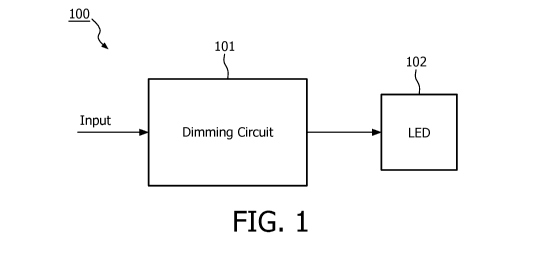
[0023] Fig. 1 illustrates a simplified block diagram of a lighting fixture
in accordance with a
representative embodiment.
[0024] Fig. 2 illustrates a simplified schematic diagram of a dimming
circuit in accordance
with a representative embodiment.
[0025] Fig. 3 illustrates a simplified schematic diagram of a dimming
circuit in accordance
with another representative embodiment.
Detailed Description
[0026] In the following detailed description, for purposes of explanation
and not limitation,
representative embodiments disclosing specific details are set forth in order
to provide a
thorough understanding of the present teachings. Descriptions of known
devices, materials
and manufacturing methods may be omitted so as to avoid obscuring the
description of the
example embodiments. Nonetheless, such devices, materials and methods that are
within the
purview of one of ordinary skill in the art may be used in accordance with the
representative
embodiments.
CA 02771975 2012-02-23
WO 2011/024101 PCT/1B2010/053729
- 9 -
[0027] Fig. 1 illustrates a simplified block diagram of a lighting
apparatus 100 in accordance
with various embodiments of the invention. The lighting apparatus includes a
dimming circuit
101, which receives an input voltage, such as a line voltage. Based on a
desired dimmer setting,
the dimming circuit 101 provides a particular drive current to an LED 102. In
a representative
embodiment, the lighting apparatus may be provided in a housing with the
dimming circuit and
LED in a common or separate package.
[0028] Fig. 2 illustrates a simplified schematic diagram of a dimming
circuit 200 in
accordance with a representative embodiment. The dimming circuit 200 is
contemplated for
use as the dimming circuit 101 of lighting fixture 100 in Fig. 1. The dimming
circuit 200
comprises a constant current converter ('converter') 201 and a controller 202.
The controller
102 receives a dimming input and the converter 101 receives an input voltage.
In a
representative embodiment, the converter 201 is a known power supply
configured to receive
an input from one of a variety of known power sources which are illustratively
an AC voltage
(line voltage), a DC voltage or low voltage AC source. The converter 201
provides an output
current based on the input voltage. As described more fully herein, a PWM
signal 203 is
provided to a shunt switch (e.g., a field effect transistor (FET)) 110 (Q1).
[0029] In a representative embodiment, the controller 202 includes a known
microprocessor
comprising memory and logic, and is configured to receive the dimming input
and to provide a
PWM signal 203 and a reference voltage (V,f) 204. The use of a microprocessor
is merely
illustrative, and the use of a programmable logic device (PLD) such as a field
programmable
gate array (FPGA), or an application specific integrated circuit (ASIC), or
discrete electronic
components are also contemplated for use in the controller 202.
[0030] The reference voltage (V,f) 204 provides one input to an error
amplifier circuit 205.
Current to the LEDs flows through a sensing resistor (R1) 211, which produces
a sense voltage
that is provided as another input to the error amplifier circuit 205. The
error amplifier circuit
205 compares the sense voltage signal to the reference voltage (\ire) 204. A
feedback signal
206, which is based on the output of the error amplifier circuit 205, is
provided to the converter
201. In response to the value of the feedback signal 206, the converter 201
increases or
CA 02771975 2012-02-23
WO 2011/024101 PCT/1B2010/053729
- 10 -
decreases the current to the LEDs until the sensed voltage at sensing resistor
(R1) 211 is
substantially identical to the reference voltage (Vref) 204.
[0031] In operation, the converter 201 provides a comparatively constant
current to a first
inductor 207 (L1). The current from the converter 201 in turn flows to a
second inductor (L2)
208. The second inductor (L2) 208 in conjunction with capacitor (C1) 209
beneficially reduces
current ripple and provides a substantially constant DC current to either the
LEDs (not shown in
Fig. 2) or to the shunt switch (Q1) 210. Capacitor (C1) 209 and second
inductor (L2) 208 have
respective values selected so that the switching of shunt switch 210 (Q1) does
not significantly
alter the voltage at capacitor 209 (C1), and so the current in the second
inductor (L2) 208
remains substantially constant. This nearly constant current then flows either
to the LEDs
directly or through the shunt switch (Q1) 210.
[0032] The current flow to either the LEDs directly or to the shunt switch
210 (Q1) depends
on the level of dimming provided at the dimming input to the controller 202.
Often, in order to
avoid color level shifts and to provide a base level of efficiency, a minimum
current amplitude is
specified. This minimum current amplitude is often expressed in terms of a
percentage of a
maximum current level or amplitude through the LED junction. For example, an
LED
manufacturer or lamp manufacturer may specify a minimum current amplitude
required of the
LEDs as percentage of a maximum current amplitude that can be delivered to the
LEDs.
[0033] For illustrative purposes, suppose this minimum currently is
approximately 10% of
the maximum current amplitude of the LEDs used in the lighting fixture 100. It
is emphasized
that the percentage of the maximum current amplitude may be less than or
greater than 10%,
and this value is selected only for ease of explanation. In accordance with
the representative
embodiment described in connection with Fig. 2, when the dimming input to the
controller 202
is between 100% of this maximum current level to 10% of the maximum current
level, the PWM
signal 203 output from the controller 202 is at a voltage that reverse biases
the shunt switch
210 (Q1) so that it is not conducting and is 'off', and the reference voltage
(Vref) 204 is at a
level proportional to the dimming input. The reference voltage (Vref) 204 is
input to error
amplifier circuit 205 and provides a feedback 206 to the converter 201 that is
proportional to
the error signal between the desired current set point (reference voltage
(Vref) 204) and the
CA 02771975 2012-02-23
WO 2011/024101 PCT/1B2010/053729
- 11 -
actual LED current sensed across sensing resistor (R1) 211. The feedback 206
is input to the
converter 201, and the output from the converter 201 is an analog output that
provides the
desired current level to the LED.
[0034] By contrast, and keeping with the illustrative values, when the
dimming input to the
controller 202 is approximately 10% or less (to approximately 0%), the
controller 202 provides
the reference voltage (Vref) 104 of 10% (or less, as selected) of the maximum
value. The PWM
signal 203 to the shunt switch (Q1) 210 selectively biases the shunt switch
(Q1) 210 on at a set
duty cycle. In the present representative embodiment with a threshold level of
10% of the
maximum LED drive current, the PWM signal 203 has an off duty cycle that
substantially
matches the desired dim level divided by 10 (since the average current is
already reduced to
10%). For example, a PWM off duty cycle of 1% corresponds to a dim level of
0.1%.
[0035] Beneficially, because the shunt switch (Q1) 210 is forward biased
(turned 'on') only
when the current through the first inductor (L1) 207 and the second inductor
(L2) 208 are
reduced to a level at or below a selected fraction (e.g., 10% or less) of the
maximum current
level, losses in the shunt (Q1) 210 are minimized. In addition, the circuit
200 allows the shunt
switch (Q1) 210 to have a comparatively high resistance, and in turn a
comparatively low
capacitance. This reduces the likelihood of switching losses in case a
comparatively high PWM
frequency is desired. To this end, in an illustrative embodiment, the shunt
switch (Q1) 210 is a
metal oxide semiconductor field effect transistor (MOSFET) with a voltage
rating of 600V
(assuming the LED system is high voltage output), has a resistance of
approximately 1.20, and
an output capacitance of approximately 100pF. If the shunt switch (Q1) 210 of
the present
example (i.e., a MOSFET) would conduct the entire current (e.g., 1A) from the
converter 101,
the conduction loss alone would be already 1W at the point where the on-time
of shunt switch
(Q1) 210 is near 100%. As can be appreciated, such loss is not desirable. By
contrast, and in
accordance with representative embodiments, if the current through the shunt
switch (Q1) 210
is limited to 10% or less than the maximum current level, the conduction loss
of the same
MOSFET is significantly lower; illustratively 0.012W under the same conditions
and parameters.
Because of this significant reduction in conduction losses the resistance of
the shunt switch 210
(Q1) may be selected to be greater. Continuing with the same example, if the
shunt switch 210
CA 02771975 2012-02-23
WO 2011/024101 PCT/1B2010/053729
- 12 -
(Q1) were a MOSFET with higher resistance (e.g. 100) the output capacitance
would drop
significantly (e.g., a factor of 10 in the present example). Beneficially, the
conduction losses
and switching losses are significantly reduced (by a factor of 10 in the
present example), and
the switching time is also reduced due to the reduced capacitance. Notably,
reducing the
switching time of the shunt switch (Q1) 210 may be especially beneficial
because comparatively
precise dimming control benefits from comparatively fast switching
transitions, which are
effected by providing a switch (e.g., shunt switch 210 (Q1) with a
comparatively low
capacitance, in the representative embodiments. In addition, a MOSFET with 10
times the on-
resistance is much less expensive than a lower resistance FET.
[0036] Notably, the frequency of the PWM signal 203 provided to the shunt
switch (Q1) 210
can be selected to optimize performance of the circuit 200. In practice, it is
desired to have a
substantially constant current in first inductor (L1) 207 and substantially
constant voltage across
the capacitor (C1) 109 while the shunt switch (Q1) 110 turns on and off at a
fixed duty cycle in
response to the PWM signal 203. This ensures that the current in the LEDs is
proportional to
the duty cycle of the shunt switch, or to the inverse duty cycle. In
accordance with a
representative embodiment, these conditions are achieved by choosing a
sufficiently high PWM
frequency for the shunt switch (Q1) 210. In a representative embodiment, the
power supplies
are isolated, and beneficially the converter 101, which provides isolation,
never stops switching
and, therefore, continuously provides sufficient power to any auxiliary supply
windings needed
to drive the current feedback amplifiers and dimming interface controllers as
the minimum
converter output current is fixed at a non-zero minimum level (e.g., 10% or
less of max in the
above example). The frequency of the PWM signal 203 for LEDs is typically
chosen to be in the
order of a 200Hz to 5 kHz. However, to reduce the size of the second inductor
L2 (209) and the
capacitor (C1) 210, it is possible to operate the shunt switch (Q1) 210 at
even higher
frequencies. This is especially the case when the shunt switch (Q1) 210 is a
relatively high
resistance, low capacitance device that allows the fast switching transitions.
[0037] Fig. 3 illustrates a simplified schematic diagram of a dimming
circuit 300 in
accordance with another representative embodiment. The dimming circuit 300 is
contemplated for use as the dimming circuit 101 of lighting fixture 100 in
Fig. 1. Many of the
CA 02771975 2016-11-28
56146-90
- 13 -
details of the components described in connection with the embodiments of the
dimming
circuit 200 illustrated in Fig. 2 are common to the embodiments of the dimming
circuit 300.
Many of these common details are not repeated in order to avoid obscuring the
description of
the presently described embodiments. Moreover, like the embodiments described
in
connection with Fig. 2, the dimming circuit 300 provides efficient dimming of
LED's over the
entire dim range of approximately 0% to approximately 100%. Like dimming
circuit 200,
dimming circuit 300 provides analog dimming from converter 201 to a threshold
level that
ensures proper LED operation with minimal color shift.
[0038] The dimming circuit 300 comprises converter 201 and controller 202.
The controller
202 receives a dimming input and the converter 201 receives an input voltage,
such as an AC
line voltage. In a representative embodiment, the controller 202 comprises a
known
microprocessor comprising memory and logic and is configured to receive the
dimming input
and provide PWM signal 203 and reference voltage (Vref) 204. The use of a
microprocessor is
merely illustrative, and the use of a programmable logic device (PLD) such as
a field
programmable gate array (FPGA) or an application specific integrated circuit
(ASIC) are also
contemplated for use in the controller 202. The reference voltage (Vref) 204
comprises one
input to an amplifier circuit 205.
[0039] The dimming circuit 300 comprises a buck converter 301 that pulse-
width modulates
the output current from a threshold level (e.g., 10% of the maximum current
amplitude to the
LED) to 0% current, or 100% dimming. The buck converter 301 comprises a first
switch (Q1)
302 in parallel with a second switch (Q2) 303, an inductor 304 and a resistor
305. A diode (D1)
306 is provided between the output of the second switch 303 (02) and an input
to the error
amplifier circuit 205. The buck-converter 301 may be as described in commonly
owned US
Patent Application Publication 20080278092 entitled "HIGH POWER FACTOR LED-
BASED
LIGHTING APPARATUS AND METHODS" to Lys, et al. In accordance with
representative
embodiments, the buck converter 301 can either operate at high frequency
compared to the
frequency PWM signal 203 and use a known control method, or use a hysteretic
or peak
current control method to obtain comparatively fast and comparatively precise
current control.
CA 02771975 2012-02-23
WO 2011/024101 PCT/1B2010/053729
- 14 -
The switching frequency of the buck converter 301 is illustratively in the
range of approximately
100 kHz to approximately 500 kHz. Switching losses are low if the capacitance
of the second
switch (Q2) 303 and the diode (D1) 306 are comparatively small (on the order
of 101 pF). This
can be accomplished if the on-resistance of the second switch (Q2) 303 is
chosen high enough
and the current rating of the diode (D1) 306 is chosen low enough. As such, in
accordance with
representative embodiments, the current through the buck converter 301 is
maintained at a
comparatively low amplitude first (e.g., 10% or less of the maximum current of
the LEDs), which
allows the selection of the on-resistance of the second switch (Q2) 303 to be
comparatively
high, and which allows comparatively low current across the diode (D1) 306
without significant
conduction losses. For example, a diode with a current rating of 1 A might
have a junction
capacitance of 20pF-50pF; whereas a diode (e.g., diode (D1) 306) with a
current rating of 0.1A
might have a junction capacitance in the range of approximately 1 pF to
approximately 5pF,
which is comparatively low. The switching losses are proportional to
frequency, so a factor of
reduction in capacitance translates to a factor of 10 reduction in switching
losses, which can
be very significant at operating frequencies of 100 kHz to500kHz.
[0040] In accordance with representative embodiments the buck converter 301
is operated
at a comparatively high switching frequency to allow low output current ripple
into the LEDs
(i.e. substantially constant LED current) with a small value of the inductor
304 (L2). Notably,
incorporating a comparatively small value inductance in the inductor 304 (L2)
will determine
how quickly the inductor 304 (L2) can discharge during the "off" PWM cycle.
Basically, the
inductor 304 (L2) determines the switching speed of the PWM cycle and,
therefore, the
maximum frequency of the PWM signal 203 and the rise time and fall time of the
PWM signal
203. As such, the inductor 304 (L2) of the buck converter 301 determines the
dimming
resolution and minimum dimming level achievable in the dimming circuit 300.
[0041] Notably, however, the frequency of the PWM signal 203 cannot be
chosen arbitrarily
small. At PWM frequencies on the order of approximately 100Hz might result in
visible flicker;
and even PWM frequencies as low as 500Hz can be a problem for photography. As
such, in
accordance with representative embodiments, in order to avoid detectable
flicker and to
provide a better output light quality of the LEDs the frequency of the PWM
signal is set above a
CA 02771975 2012-02-23
WO 2011/024101
PCT/1B2010/053729
- 15 -
threshold level. In practice, the buck converter 301 operates at a frequency
at least 100 times
higher than the PWM frequency to enable a PWM duty cycle of approximately 5%
with
acceptable accuracy. For lower dim levels, an even higher buck frequency is
necessary.
[0042] In
keeping with the illustrative range described above, the analog dimming may be
implemented from dimming from approximately 0% dimming (i.e., no dimming, and
100% of
the maximum current amplitude to the LED) down to 90% dimming (i.e., 10% of
the maximum
current amplitude to the LED). Below 90% dimming, a high frequency buck
converter 301 is
used to PWM the output current from 10% to 0%. Notably, however, the buck
converter 201
allows the threshold level to be set at approximately 5% of the maximum
current amplitude to
the LEDs. As noted above, the buck converter 201 can either operate at very
high frequency as
compared to the PWM frequency and use a standard control method or use a
hysteretic or
peak current control method to obtain very fast and precise current control.
The buck
converter 201 can be by-passed with a switch (FET or otherwise) during the
analog dimming
portion where the primary current control is used to minimize any additional
losses at full
output. The first switch (Q1) 302, which is a bypass switch, can be one of a
variety of
controllable switches (e.g., a FET) and, in the present embodiment, can be a
comparatively slow
switching device as it only needs to turn on above 10% dim (for example) and
is off below this
level. The first switch (Q1) 302 can be have a comparatively low on-
resistance. The
capacitance of first switch (Q1) 302 is of minor consideration in circuit
design because there are
low switching losses in first switch (Q1) 302. In particular, in
representative embodiments, the
dim command is relatively fixed and changes only when the user changes a set
point. For
instance and continuing with the same example, if a dimming command of 11% of
the
maximum current is given, then first switch (Q1) 302 is 'on' and converter 201
provides the
constant current of 11% to the LEDs. Note that the first switch (Q1) 201 never
turns off in this
condition and the second switch (Q2) 303 never turns on, so there are no
switching losses. By
contrast, for example if the dim command is 9% of the maximum current is
given, then the first
switch (Q1) 302 is 'off' and the buck converter 301 provides the constant
current control. In
this range of operation, the first switch (Q1) is not switching but rather is
'off.' Again there are
no switching losses contributed by the first switch (Q1) 302.
CA 02771975 2012-02-23
WO 2011/024101 PCT/1B2010/053729
- 16 -
[0043] In operation, based on the dimming input, the controller 201
provides the reference
voltage (Vref) 204 and the PWM signal 203. When the reference voltage (Vref)
204 is above a
dimming threshold (e.g., 10% of the maximum current amplitude to the LEDs) the
first switch
(Q1) 302, which functions as a shunt switch, of the buck converter 301 is
biased to conduct (i.e.,
is 'on') by the converter 201. Thus for dimming inputs to the controller 202
of 0% dimming (i.e.,
maximum current amplitude to the LEDs) to the minimum analog dim setting (10%
of the
maximum current amplitude as an example), Buck converter 301 produces a
regulated output
current to the LEDs via the first switch (Q1) 302. The remaining components of
the buck
converter 301, namely second switch (Q2) 203, inductor (L2) 304, resistor (R3)
305 and diode
(D1) 306 are all by-passed to minimize losses. For dimming inputs to the
controller 101 less
than the threshold (e.g., less than 10% of the maximum amplitude current to
the LED), the first
switch (Q1) 302 is not conducting, and the converter 201 regulates the voltage
across the
capacitor (Cl) 307 to a voltage greater than the turn-on LED voltage.
Accordingly, the buck
converter 301 is enabled to regulate the LED current at the 10% analog level.
In addition, the
second switch (Q2) 203 is turned on and off by the PWM 103, and thus the buck
converter 301
is then turned on and off at a fairly low PWM frequency (100Hz to1000Hz for
example) by the
controller 101. The duty cycle of the buck converter 301 is then adjusted
based on the PWM
signal, in essentially the same manner as in circuit 200 to give a PWM current
in the LEDs that is
proportional to the dim command (smaller on time at low dim and larger at off
time).
[0044] In a representative embodiment, in order to avoid any control loop
response issues,
the buck converter 301 can be controlled via hysteretic current control during
the on time to
give a comparatively fast response time with substantially no current
overshoot in the LEDs.
However, alternative current control methods such as peak current control,
standard current
mode control or critical conduction current control can be used depending on
the required
specifications. Since the buck converter 301 circuit is only active during
deep dimming (below
10% for example), the second switch (Q2) 303, the diode (D1) 306 and inductor
(L2) 304 only
need to be designed to handle the 10% current level, not the full output
current. This also
allows one to choose a switch (e.g., a MOSFET) and diode with comparatively
small capacitance
that allows fast switching frequency of the buck converter 301 without
excessive losses. Finally,
CA 02771975 2012-02-23
WO 2011/024101 PCT/1B2010/053729
- 17 -
the buck converter 301 can be placed in the positive LED current connection as
shown or the
negative side to make driving of the FET simpler (ground referenced). Other
configurations
within the purview of one of ordinary skill in the art are contemplated.
[0045] While several inventive embodiments have been described and
illustrated herein,
those of ordinary skill in the art will readily envision a variety of other
means and/or structures
for performing the function and/or obtaining the results and/or one or more of
the advantages
described herein, and each of such variations and/or modifications is deemed
to be within the
scope of the inventive embodiments described herein. More generally, those
skilled in the art
will readily appreciate that all parameters, dimensions, materials, and
configurations described
herein are meant to be exemplary and that the actual parameters, dimensions,
materials,
and/or configurations will depend upon the specific application or
applications for which the
inventive teachings is/are used. Those skilled in the art will recognize, or
be able to ascertain
using no more than routine experimentation, many equivalents to the specific
inventive
embodiments described herein. It is, therefore, to be understood that the
foregoing
embodiments are presented by way of example only and that, within the scope of
the
appended claims and equivalents thereto; inventive embodiments may be
practiced otherwise
than as specifically described and claimed. Inventive embodiments of the
present disclosure
are directed to each individual feature, system, article, material, kit,
and/or method described
herein. In addition, any combination of two or more such features, systems,
articles, materials,
kits, and/or methods, if such features, systems, articles, materials, kits,
and/or methods are not
mutually inconsistent, is included within the inventive scope of the present
disclosure.
[0046] All definitions, as defined and used herein, should be understood to
control over
dictionary definitions, definitions in documents incorporated by reference,
and/or ordinary
meanings of the defined terms.
[0047] The indefinite articles "a" and "an," as used herein in the
specification and in the
claims, unless clearly indicated to the contrary, should be understood to mean
"at least one."
The phrase "and/or," as used herein in the specification and in the claims,
should be
understood to mean "either or both" of the elements so conjoined, i.e.,
elements that are
conjunctively present in some cases and disjunctively present in other cases.
Multiple elements
CA 02771975 2012-02-23
WO 2011/024101 PCT/1B2010/053729
- 18 -
listed with "and/or" should be construed in the same fashion, i.e., "one or
more" of the
elements so conjoined. Other elements may optionally be present other than the
elements
specifically identified by the "and/or" clause, whether related or unrelated
to those elements
specifically identified.
[0048] As used herein in the specification and in the claims, "or" should
be understood to
have the same meaning as "and/or" as defined above. For example, when
separating items in a
list, "or" or "and/or" shall be interpreted as being inclusive, i.e., the
inclusion of at least one,
but also including more than one, of a number or list of elements, and,
optionally, additional
unlisted items. Only terms clearly indicated to the contrary, such as "only
one of" or "exactly
one of," or, when used in the claims, "consisting of," will refer to the
inclusion of exactly one
element of a number or list of elements. In general, the term "or" as used
herein shall only be
interpreted as indicating exclusive alternatives (i.e. "one or the other but
not both") when
preceded by terms of exclusivity, such as "either," "one of," "only one of,"
or "exactly one of."
"Consisting essentially of," when used in the claims, shall have its ordinary
meaning as used in
the field of patent law.
[0049] Any reference numerals or other characters, appearing between
parentheses in the
claims, are provided merely for convenience and are not intended to limit the
claims in any
way.
[0050] It should also be understood that, unless clearly indicated to the
contrary, in any
methods claimed herein that include more than one step or act, the order of
the steps or acts
of the method is not necessarily limited to the order in which the steps or
acts of the method
are recited.
[0051] In the claims, as well as in the specification above, all
transitional phrases such as
"comprising," "including," "carrying," "having," "containing," "involving,"
"holding," "composed
of," and the like are to be understood to be open-ended, i.e., to mean
including but not limited
to. Only the transitional phrases "consisting of" and "consisting essentially
of" shall be closed
or semi-closed transitional phrases, respectively.
[0052] What is claimed is: