Note: Descriptions are shown in the official language in which they were submitted.
CA 02772056 2012-02-23
WO 2011/029012 PCT/US2010/047829
- 1 -
METHODS FOR FORMING FOAMED ELECTRODE STRUCTURES
Cross-Reference to Related Application
[0001] This application claims the benefit of United
States Provisional Application No. 61/239,910, filed
September 4, 2009, which is hereby incorporated by
reference herein in its entirety.
Field of the Invention
[0002] The present invention relates to forming
electrodes, and more particularly. to processing
techniques for creating electrode structures containing
an electronically conductive foam and an electronically
conductive substrate.
Background of the Invention
[0003] Electrodes are used to supply and remove
electrons from some medium, and are typically
manufactured from metals or metal alloys.
Electrochemical cells use electrodes to facilitate
electron transport and transfer during electrochemical
interactions. Batteries, or electrochemical storage
devices, may use electrodes in both galvanic and
electrolytic capacities, corresponding to discharging
CA 02772056 2012-02-23
WO 2011/029012 PCT/US2010/047829
2 -
or charging processes, respectively. Electrochemical
reactions generally occur at or near the interfaces of
an electrolyte and the electrodes, which may extend to
an external circuit through which electric power can be
applied or extracted.
[0004] Electrodes are typically placed in contact-
with current collectors in order to draw and/or supply
electrical power. In order to reduce system losses,
there must be sufficient electrical contact at the
interface between the electrode and the current
collector. The quality of this interface may depend on
the processing steps used to manufacture the electrode
and the current collector, and the assembly steps used
to place the two components in electrical contact.
[0005] Numerous processing steps, which include both
mechanical and chemical interactions, are typically
required to manufacture the electrodes and current
collectors that accomplish the aforementioned assembly.
These numerous processing steps, often using multiple
subassemblies, may increase cost, increase
infrastructure requirements, and introduce
opportunities for manufacturing errors to occur.
Accordingly, it would be desirable to reduce and/or
consolidate the processing steps required to
manufacture electrode structures.
Summary of the Invention
[0006] In view of the foregoing, provided are
techniques, compositions, and arrangements for forming
electrode structures that include one or more
electronically conductive foams in contact with one or
more electronically conductive substrates. In some
embodiments the present invention provides techniques
CA 02772056 2012-02-23
WO 2011/029012 PCT/US2010/047829
3 -
for forming electronically conductive foams directly on
an electronically conductive substrate. In some
approaches, forming electronically conductive foams
directly on an electronically conductive substrate may
reduce, consolidate, or both, the process steps for
forming electrode structures.
[0007] In some embodiments, a precursor material may
be placed in contact with an electronically conductive
substrate (e.g., metal), where an interface may exist
between a surface of the substrate and the precursor
material. -The precursor material may be a polymer
foam, polymer slurry, dried polymer slurry, any other
suitable precursor material or any suitable combination
thereof. In some embodiments, the precursor material
in contact with the substrate may be further processed
(e.g., dried, cured) while in contact with the
substrate. For example, a plating or coating process
may be applied to the subassembly of the precursor
material and substrate in contact with one another.
The plating or coating process may include coating all
or part of the precursor material and substrate with an
electronically conductive material (e.g., metal) to
form an electronically conductive network throughout
the volume of the precursor material. The plated
precursor material, as well as one or more components
of-the plated precursor material, may be substantially
removed (e.g., pyrolyzed), thereby leaving an
electronically conductive foam in contact with the
substrate. In some embodiments, active materials may
be included in the precursor material, or the active
materials may be introduced to the electronically
conductive foam, or both. In some embodiments, the
electronically conductive foam may be sintered at
CA 02772056 2012-02-23
WO 2011/029012 PCT/US2010/047829
- 4 -
elevated temperature. The substrate and foam may be of
any suitable shape, including flat plate, curved plate,
dome, or any other suitable shape or combination
thereof.
[0008] In some embodiments, a plurality of first
particles may be combined with a plurality of second
particles and a liquid agent to form a slurry. The
slurry may include at least one electronically
conductive component and at least one electronically
nonconductive component including, but not limited to,
one or more of polymer particles, binders, liquid
agents, any other suitable electronically nonconductive
material or any suitable combination thereof. At least
one contiguous layer of the slurry may be formed on a
surface of an electronically conductive substrate. The
layers may be uniform or non-uniform in thickness and
may be contiguous or non-contiguous on the surface of
the substrate. In some embodiments, more than one
contiguous layer may be formed on a surface of the
substrate.
[0009] Substantially all (i.e., all or almost all) of
the liquid agent may be removed from the at least one
contiguous layer of the slurry to leave a solid
composite material, where the solid composite material
may remain in contact with the surface of the
substrate. For example, the liquid agent may be
removed by drying, heating, any other suitable removal
process, or any combination thereof. Substantially all
of the plurality of first particles may be removed from
the composite material (e.g., pyrolyzed), where the
remaining plurality of second particles may form a
corresponding electronically conductive foam in contact
with the substrate.
CA 02772056 2012-02-23
WO 2011/029012 PCT/US2010/047829
- 5 -
(0010] In some embodiments, a composite material may
be placed in contact with an electronically conductive
substrate. The composite material may include at least
.one electronically conductive component and at least
one electronically nonconductive component including,
but not limited to, one or more of a polymer foam,
dried polymer slurry, any other suitable electronically
nonconductive material or any suitable combination
thereof. The composite material may be a composite
slurry including two or more types of particles. For
example, the composite material may be a slurry
including a liquid agent (e.g., organic solvent),
electronically conductive particles (e.g., metal) and
electronically nonconductive particles (e.g., polymer).
In some embodiments, the composite slurry may be
further processed (e.g., dried, cured) while in contact
with the substrate. The electronically nonconductive
components, or any other components, may be
substantially removed (e.g., pyrolyzed) from the dried
composite slurry, thereby leaving an electronically
conductive foam in contact with the substrate.
Brief Description of the Drawings
[0011] FIG. 1 shows a schematic cross-sectional view
of an illustrative structure of a bi-polar electrode-
unit (BPU) in accordance with some embodiments of the
present invention;
[0012] FIG. 2 shows a schematic cross-sectional view
of an illustrative-structure of a'stack of BPUs of FIG.
1 in accordance with some embodiments of the present
invention;
[0013] FIG. 3 shows a schematic cross-sectional view
of an illustrative structure of a mono-polar electrode-
CA 02772056 2012-02-23
WO 2011/029012 PCT/US2010/047829
- 6 -
unit (MPU) in accordance with some embodiments of the
present invention;
[0014] FIG. 4 shows a schematic cross-sectional view
of an illustrative structure of a device containing two
MPUs of FIG. 3 in accordance with some embodiments of
the present invention;
[0015] FIG. 5 shows a cubic section of an
illustrative solid-phase foam in accordance with some
embodiments of the present invention;
[0016] FIG. 6 shows an illustrative electrode
structure with a cutaway section in accordance with
some embodiments of the present invention;
[0017] FIG. 7 shows an illustrative flow diagram for
creating an electrode structure in accordance with some
embodiments of the present invention;
(0018] FIG. 8 shows an illustrative flow diagram for
creating an electrode structure in accordance with some
embodiments of the present invention;
[0019] FIG. 9 shows an illustrative flow diagram for
creating an electrode structure in accordance with some
embodiments of the present invention;
(0020] FIG. 10 shows an illustrative flow diagram
for creating an electrode structure in accordance with
some embodiments of the present invention;
[0021] FIG. 11 shows an illustrative side elevation
view of a precursor material in contact with a
substrate in accordance with some embodiments of the
present invention;
(0022] FIG. 12 shows an illustrative top plan view
of the elements of FIG. 11, taken from line XII-XII, in
accordance with some embodiments of the present
invention;
CA 02772056 2012-02-23
WO 2011/029012 PCT/US2010/047829
7 -
(0023] FIG. 13 shows an illustrative partial cross-
sectional view of an interface between a precursor
material and a substrate in accordance with some
embodiments of the present invention;
[0024] FIG. 14 shows an illustrative partial cross-
sectional view of the interface of FIG. 13, coated with
an electronically conductive material in accordance
with some embodiments of the present invention;
[0025] FIG. 15 shows an illustrative partial cross-
sectional view of the interface of FIG. 14 in
accordance with some embodiments of the present
invention;
[0026] FIG. 16 shows an illustrative side elevation
view of a composite material in contact with a
substrate in accordance with some embodiments of the
present invention;
[0027] FIG. 17 shows an illustrative top plan view
of the elements of FIG. 16, taken from line XVII-XVII,
in accordance with some embodiments of the present
invention;
(0028] FIG. 18 shows an illustrative partial cross-
sectional view of an interface between a composite
material and'a substrate in accordance with some
embodiments of the present invention;
[0029] FIG. 19 shows an illustrative partial cross-
sectional view of an interface between an
electronically conductive foam-and a substrate in
accordance with some embodiments of the present
invention;
[0030] FIG. 20 shows an illustrative partial cross-
sectional view of an interface between a composite
material and a substrate in accordance with some
embodiments of the present invention; and
CA 02772056 2012-02-23
WO 2011/029012 PCT/US2010/047829
8 -
[0031] FIG. 21 shows an illustrative partial cross-
sectional view of an interface between an
electronically conductive foam and a substrate in
accordance with some embodiments of the present
invention.
Detailed Description of the Invention
[0032] The present invention provides methods,
compositions, and arrangements for forming electrode
structures that include one or more electronically
conductive foams in contact with one or more
electronically conductive substrates. The present
invention provides methods, compositions, and
arrangements for forming electronically conductive
foams directly on an electronically conductive
substrate. The electrode structures and assemblies of
the present invention may be applied to energy storage
devices such as, for example, batteries, capacitors or
any other energy storage device which may store or
provide electrical energy or current, or any
combination thereof. For example, the electrode
structures and assemblies of the present invention may
be implemented in a mono-polar electrode unit (MPU) or
a bi-polar electrode unit (BPU), and may be applied to
one or more surfaces of the MPU or BPU. It will be
understood that while the present invention is
described herein in the context of stacked energy
storage devices, the concepts discussed are applicable
to any intercellular electrode configuration including,
but not limited to, parallel plate, prismatic, folded,
wound and/or bipolar configurations, any other suitable
configurations or any combinations thereof.
CA 02772056 2012-02-23
WO 2011/029012 PCT/US2010/047829
- 9 -
[0033] In some embodiments, electrodes may contain
porous structures or conductive foams to increase
interface area, which may improve transport of
compounds such as molecules (e.g., water) or ions
(e.g., hydroxyl ions), or both. Electrochemical
reactions may occur at or near interfaces between an
active material, an electrolyte and an electronically
conducting component. Increased interface area may
allow increased charge or discharge rates for
electrochemical devices. In some embodiments, the
disclosed techniques, compositions, and arrangements
may provide electrodes having porous structures or
conductive foams in contact with suitable substrates.
[0034] The present disclosure includes methods,
compositions, and arrangements for forming
electronically conductive electrodes in contact with
electronically conductive substrates. The electrode
may be formed, for example, by coating a porous
precursor material with electronically conductive
.20 material, or removing one or more components of a solid
composite material, or both. In some embodiments,
electronically conductive networks or foams may be
formed directly on one or more surfaces of a substrate.
(0035] The invention will now be described in the
context of FIGS. 1-21, which show illustrative
embodiments.
[0036] FIG. 1 shows a schematic cross-sectional view
of an illustrative structure of BPU 100 in accordance
with some embodiments of the present invention.
Exemplary BPU 100 may include a positive active
material electrode layer 104, an electronically
conductive, impermeable substrate 106, and a negative
active material electrode layer 108. Positive
CA 02772056 2012-02-23
WO 2011/029012 PCT/US2010/047829
- 10 -
electrode layer 104 and negative electrode layer 108
are provided on opposite sides of substrate 106.
[0037] FIG. 2 shows a schematic cross-sectional view
of an illustrative structure of stack 200 of BPUs 100
of FIG. 1 in accordance with some embodiments of the
present invention. Multiple BPUs 202 may be arranged
into stack configuration 200. Within stack 200,
electrolyte layer 210 is provided between two adjacent
BPUs, such that positive electrode layer 204 of one BPU
is opposed to negative electrode layer 208 of an
adjacent BPU, with electrolyte layer 210 positioned
between the BPUs. A separator may be provided in one
or more electrolyte layers 210 to electrically separate
opposing positive and negative electrode layers. The
separator allows ionic transfer between the adjacent
electrode units for recombination, but may
substantially prevent electronic transfer between the
adjacent electrode units. As defined herein, a "cell"
or "cell segment" 222 refers to the components included
in substrate 206 and positive electrode layer 204 of a
first BPU 202, negative electrode layer 208 and
substrate 206 of a second BPU 202 adjacent to the first
BPU 202, and electrolyte layer 210 between the first
and second BPUs 202. Each impermeable substrate,206 of
each cell segment 222 may be shared by applicable
adjacent cell segment 222.
[0038]. FIG. 3 shows a schematic cross-sectional view
of an illustrative structure of MPU 300 in accordance
with some embodiments of the present invention.
Exemplary MPU 300 may include active material electrode
layer 304 and electronically conductive, impermeable
substrate 306. Active material layer 304 may be any
suitable positive or negative active material.
CA 02772056 2012-02-23
WO 2011/029012 PCT/US2010/047829
- 11 -
[0039] FIG. 4 shows a schematic cross-sectional view
of an illustrative structure of a device containing two
MPUs of FIG. 3 in accordance with some embodiments of
the present invention. Two MPUs 300 having a positive
and negative active material, respectively, may be
stacked to form electrochemical device 400.
Electrolyte layer 410 may be provided between two MPUs
300, such that positive electrode layer 404 of one MPU
300 is opposed to negative electrode layer 408 of the
other MPU 300, with electrolyte layer 410 positioned
between the MPUs. A separator may be provided
electrolyte layers 410 to electrically separate
opposing positive and negative electrode layers
Although not shown, in some embodiments two MPUs having
positive and negative active material, respectively,
may be added to stack 20,0, along with suitable layers
of electrolyte, to form a bi-polar battery. Bi-polar
batteries and battery stacks are discussed in more
detail in Ogg et al. U.S. Patent Application No.
11/417,489, Ogg et al. U.S. Patent Application No.
12/069,793, and West et al. U.S. Patent Application No.
12/258,854, all of which are hereby incorporated by
reference herein in their entireties.
[0040] The substrates used to form electrode units
(e.g., substrate 106, 206, 406, 416) may be formed of
any suitable electronically conductive and impermeable
or substantially impermeable material, including, but
not limited to, a non-perforated metal fbil, aluminum
foil, stainless steel foil, cladding material including
nickel and aluminum, cladding material including copper
and aluminum, nickel plated steel, nickel plated
copper, nickel plated aluminum, gold, silver, any other
suitable electronically conductive and impermeable
CA 02772056 2012-02-23
WO 2011/029012 PCT/US2010/047829
- 12 -
material or any suitable combinations thereof. In some
embodiments, substrates may be formed of one or more
suitable metals or combination of metals (e.g., alloys,
solid solutions, plated metals). Each substrate may be
made of two or more sheets of metal foils adhered to
one another, in certain embodiments. The substrate of
each BPU may typically be between 0.025 and 5
millimeters thick, while the substrate of each MPU may
be between 0.025 and 30 millimeters thick and act as
terminals or sub-terminals to the ESD, for example.
Metalized foam, for example, may be combined with any
suitable substrate material in a flat metal film or
foil, for example, such that resistance between active
materials of a cell segment may be reduced by expanding
the conductive matrix throughout the electrode.
[0041] The positive electrode layers provided on
these
substrates to form the electrode units of the invention
(e.g., positive electrode layers 104, 204 and 404)
may be formed of any suitable active material,
including,
but not limited to, nickel hydroxide (Ni(OH)2), zinc
(Zn), any other suitable material, or combinations
thereof, for example. The positive active material may
be sintered and impregnated, coated with an aqueous
binder and pressed, coated with an organic binder and
pressed, or contained by any other suitable technique
for containing the positive active material with other
supporting chemicals in a conductive matrix. The
positive electrode layer of the electrode unit may have
particles, including, but not limited to, metal hydride
(MH), palladium (Pd), silver (Ag), any other suitable
material, or combinations thereof, infused in its
CA 02772056 2012-02-23
WO 2011/029012 PCT/US2010/047829
- 13 -
matrix to reduce swelling, for example. This may
increase cycle life, improve recombination, and reduce
pressure within the cell segment, for example. These
particles, such as MH, may also be in a bonding of the
active material paste, such as Ni(OH)2, to improve the
electrical conductivity within the electrode and to
support recombination.
[0042] The negative electrode layers provided on
these
substrates to form the electrode units of the invention
(e.g., negative electrode layers 108, 208, and 408)
may be formed of any suitable active material,
including,
but not limited to, MH, cadmium (Cd), manganese (Mn),
Ag, any other suitable material, or combinations
thereof, for example. The negative active material may
be sintered, coated with an aqueous binder and pressed,
coated with an organic binder and pressed, or contained
by any other suitable technique for containing the
negative active material with other supporting
chemicals in a conductive matrix, for example. The
negative electrode side may have chemicals including,
but not limited to, Ni, Zn, Al, any other suitable
material, or combinations thereof, infused within the
negative electrode material matrix to stabilize the
structure, reduce oxidation, and extend cycle life, for
example.
[0043] Various suitable binders, including, but-not
limited to, organic carboxymethylcellulose (CMC),
Creyton rubber, PTFE (Teflon), any other suitable
material or any suitable combinations thereof, for
example, may be mixed with or otherwise introduced to
the active material to maintain contact between the
CA 02772056 2012-02-23
WO 2011/029012 PCT/US2010/047829
- 14 -
active material and a=substrate, solid-phase foam, any
other suitable component, or any suitable combination
thereof. Any suitable binders may be included in
slurries or any other mixtures to increase adherence,
cohesion or other suitable property or combination
thereof.
[0044] The separator of each electrolyte layer of an
ESD may be formed of any suitable material that
electrically isolates its two adjacent electrode units
while allowing ionic transfer between those electrode
units. The separator may contain cellulose super
absorbers to improve filling and act as an electrolyte
reservoir to increase cycle life, wherein the separator
may be made of a polyabsorb diaper material, for
example. The separator may, thereby, release previously
absorbed electrolyte when charge is applied to the ESD.
In certain embodiments, the separator may be of a lower
density and thicker than normal cells so that the
inter-electrode spacing (IES) may start higher than
normal and be continually reduced to maintain the
capacity (or C-rate) of the ESD over its life as well
as to extend the life of the ESD.
(0045] The separator may bea relatively thin
material
bonded to the surface of the active material on the
electrode units to reduce shorting and improve
recombination. This separator material may be sprayed
on, coated on, pressed on, or combinations thereof, for
example. The separator may have a recombination agent
attached thereto. This agent may be infused within the
structure of the separator (e.g., this may be done by
physically trapping the agent in a wet process using a
polyvinyl alcohol (PVA or PVOH) to bind the agent to
CA 02772056 2012-02-23
WO 2011/029012 PCT/US2010/047829
- 15 -
the separator fibers, or the agent may be put therein
by electro-deposition), or it may be layered on the
surface by vapor deposition, for example. The
separator may be made of any suitable material such as,
for example, polypropylene, polyethylene, any other
suitable material or any combinations thereof. The
separator may include an agent that effectively
supports recombination, including, but not limited to,
lead (Pb), Ag, platinum (Pt), Pd, any other suitable
material, or any suitable combinations thereof, for
example. In some embodiments, an agent may be
substantially insulated from (e.g., not contact) any
electronically conductive component or material. For
example, in some arrangements the agent may be
positioned between sheets of the separator material
such that the agent does not contact electronically
conductive electrodes or substrates. While the
separator may present a resistance if the substrates of
a cell move toward each other, a separator may not be
provided in certain embodiments of the invention that
may utilize substrates stiff enough not to deflect.
[0046] The electrolyte of each electrolyte layer of
an ESD may be formed of any suitable chemical compound
that may ionize when dissolved or molten to produce an
electrically conductive medium. The electrolyte may be
a standard electrolyte of any suitable ESD, including,
but not limited to, NiMH, for example. The electrolyte
may contain additional chemicals, including, but not
limited to, lithium hydroxide (LiOH), sodium hydroxide
(NaOH), calcium hydroxide (CaOH), potassium hydroxide
(KOH), any other suitable material, or combinations
thereof, for example. The electrolyte may also contain
additives to improve recombination, including, but not
CA 02772056 2012-02-23
WO 2011/029012 PCT/US2010/047829
- 16 -
limited to, Ag(OH)2, for example. The electrolyte may
also contain rubidium hydroxide (RbOH), for example, to
improve low temperature performance. The electrolyte
may be frozen within the separator and then thawed
after the ESD is completely assembled. This may allow
for particularly viscous electrolytes to be inserted
into the electrode unit stack of the ESD before the
gaskets have formed substantially fluid tight seals
with the electrode units adjacent thereto.
(0047] Electrodes may contain an electronically
conductive network or component. The electronically
conductive network or component may reduce ohmic
resistance and may allow increased interface area for
electrochemical interactions. For example, in stack
400 shown in FIG. 4, the interface between electrolyte
410 and either positive electrode layer 404 or negative
electrode layer 408 appears to be a planar, two
dimensional surface. While a planar interface may be
employed in some embodiments of energy storage devices,
the electrode may also have porous structure. The
porous structure may increase the interface area
between electrode'and electrolyte, which may increase
the achievable charge or discharge rate. Active
materials may be mixed with or applied to the
conductive component or network to extend the interface
over a greater surface area. Electrochemical
interactions may occur at the interface between an
active material, an electrolyte, and an electronically
conductive material.
[0048] The electronically conductive substrate may
be impermeable, preventing leakage or short circuiting.
In some arrangements, one or more porous electrodes may
be maintained in contact with an electronically
CA 02772056 2012-02-23
WO 2011/029012 PCT/US2010/047829
- 17 -
conductive, non-porous substrate, as shown in FIGS. 1-
4. This arrangement may allow for electronic transfer
among an external circuit and the electrode.
[00491 As defined herein, "foam" shall mean solid-
phase porous structures, or solid-phase networks having
pores. Foams may contain voids that may be filled with
gas or vacuum, or may be partially or entirely filled
with gas, liquid, paste, particles, any other suitable
material or any combination thereof. Porosity
describes the fraction of foam volume occupied by
voids. Foams may contain more than one solid component
and may include composites of different materials.
Open cell foams refer to foams in which the pores are
interconnected. Open cell foams may allow for
molecular transport of reactants, products,
electrolytes, ions or other compounds throughout the
foam and between the foam and the surrounding
environment. Closed cell foams include pores that are
sealed off from one another, effectively preventing
transport of compounds throughout the foam. In the
following discussion, the term foam will be understood
to refer to open cell foams.
[00501 FIG. 5 shows a cubic section of illustrative
foam 500 in accordance with some embodiments of the
present invention. Solid phase component 502 may have
a plurality of pores 504 interspersed throughout,
thereby imparting porosity. Foam 500 may include a
plurality of pores 506 having a relatively smaller
spatial scale than pores 504. Pores 506 may be
characteristic of electronically conductive particles
used to create foam 500. Pores 504 may form a
substantially interconnected network throughout the
foam which may allow transport processes to occur.
CA 02772056 2012-02-23
WO 2011/029012 PCT/US2010/047829
- 18 -
Pores 504 may have any suitable shape or size
distribution. Pores 504 may have shape and size
characteristics, for example, of a precursor material
(e.g., polymer particles). The porosity of foam 500
may have any suitable value between 0 and 1, with
larger porosity being associated with values nearer to
1. Larger values of porosity may correspond to larger
values of surface area of the foam. In some
embodiments, foam 500 may include one or more
electronically conductive components (e.g., metals),
one or more active materials (e.g., Ni(OH)2), one or
more binders, any other suitable materials or any
combination thereof.
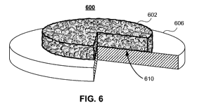
[0051] FIG. 6 shows an illustrative electrode
structure 600 with a cutaway section in accordance with
some embodiments of the present invention. Electrode
structure 600 may include foam 602 and substrate 606.
Foam 602 and substrate 606 may share interface 610 as a
plane of contact. Interface 610 represents the plane
or path in space where at least two components,.
materials or any suitable combination thereof may meet
in contact. The term "interface" as used herein shall
refer to the substantially planar area of contact
between a slurry and a substrate, a solid foam and a
substrate, any two suitable components, any suitable
component and a non-solid phase, or any other plane of
contact between two distinct materials or components.
Although shown as a planar disk geometry, electrode
structure 600 may have any suitable shape, curvature
(e.g., dome shaped), thickness (of either layer),
relative size (among substrate and foam), relative
thickness (among substrate and foam), any other
property or=any suitable combination thereof. Foam 602
CA 02772056 2012-02-23
WO 2011/029012 PCT/US2010/047829
- 19 -
and substrate 606 may have any suitable three
dimensional shape, having a cross section that may be
substantially circular, square, rectangular,
triangular, hexagonal, elliptical, and any other
suitable cross section, or combinations of shapes
thereof. For example, in some embodiments, foam 602
may be a parallelepiped with square cross section and
substrate 606 may be cylindrical. Foam 602 may include
one or more electronically conductive components (e.g.,
metals), one or more active materials (e.g., Ni(OH)2),
one or more binders, any other suitable materials or
any combination thereof. In some embodiments, active
materials may be introduced to foam 602 following
assembly or creation of structure 600.
[0052] Some exemplary techniques for creating
electronically conductive foams in contact with
electronically conductive substrates will be discussed
in the context of illustrative FIGS. 7-10 in accordance
with some embodiments of the present invention.
[0053] . FIG. 7 shows illustrative flow diagram 700
or creating an electrode structure in accordance with
ome embodiments of the present invention. Process
-tep 702 may include preparing a precursor material
such as, for example, a polymer foam. In some
embodiments, process step 702 may include making the
polymer foam by use of, for example, blowing agents.
It will be understood that any suitable technique or
combination of techniques may be used to make a polymer
foam. Process step 702 may include cleaning the
polymer foam, etching the polymer foam, adjusting the
size or shape of the polymer foam (e.g., cutting,
grinding, splitting, drilling, machining), treating the
polymer to accept an electrical charge, electrically
CA 02772056 2012-02-23
WO 2011/029012 PCT/US2010/047829
- 20 -
charging the polymer, any other suitable preparation
technique or combinations thereof. The polymer foam
may be made of carbon based polymers including but not
limited to polyurethane, polyethylene, polypropylene,
polyvinyl chloride, polystyrene, nylon, polyester,
acrylic, polycarbonate, any other suitable polymer or
combination thereof, and any suitable additives. The
polymer material may substantially maintain,its shape
characteristic of solid materials. The polymer
material may undergo pyrolysis or' carbonization at
elevated temperature.
[0054] The polymer foam may be plated or otherwise
coated with an electronically conductive material at
process step 704. The conductive coating may be any
suitable type of metal (e.g., nickel), any other
suitable electronically conductive material or any
suitable combination thereof. Process step 804 may
include electroplating, electro-less plating, chemical
vapor deposition (CVD), physical vapor deposition
(PVD), any other suitable plating or coating technique
or any suitable combination thereof. In some
embodiments, performance of processes 702 and 704 may
result in a composite foam with an electronically
conductive component or coating material. In some
embodiments, active electrode materials may be added to
the composite foam during process 704.
[0055] The polymer precursor may be removed, as
shown by process 706 in FIG. 7, following coating
process 704. Process 706 may include increasing the
temperature of the coated foam while maintaining the
foam in a reducing (e.g., forming gas, hydrogen,
humidified hydrogen, diluted hydrogen) or substantially
inert (e.g., diatomic nitrogen, argon, helium)
CA 02772056 2012-02-23
WO 2011/029012 PCT/US2010/047829
- 21 -
environment. Increased temperature in the absence of
substantial oxygen or oxygen containing compounds may
induce thermal decomposition of organic material (e.g.,
pyrolysis, carbonization) of the polymer component.
The polymer component may decompose into lighter
compounds and vaporize, desorb, or otherwise leave the
remaining components of the solid foam and enter the
gas phase. The polymer may also decompose into solid,
carbon-rich compounds or residues which may remain in
the solid foam. Process 706 may include processes that
cause some portion or substantially all of the polymer
component to decompose, carbonize, enter the gas phase,
or any combination thereof. Process 706 may remove
substantially all of the polymer component and
associated decomposition products. In some
embodiments, process step 706 may include increasing
the temperature to over 300 degrees Celsius in any
suitable environment. Process step 706 may also
include sintering or otherwise processing the remaining
electronically conductive foam at the same or different
elevated temperature, for example, to increase
conductivity, connectivity, durability, other suitable
property or any combination thereof, of the foam.
[0056] At step 708 shown in FIG. 7, an
electronically conductive, impermeable substrate may be
prepared. In some embodiments, the substrate may be
larger than the metal foam in some dimension such as,
for example, a bi-polar or mono-polar plate. In some
embodiments, the substrate may be relatively smaller
than the foam in some dimension such as, for example,
embodiments where the substrate may be one or more
tabs. The substrate may be formed of any suitable
electronically conductive and impermeable material. The
CA 02772056 2012-02-23
WO 2011/029012 PCT/US2010/047829
- 22 -
substrate may be a flat. plate of any shape (e.g.,
disk), curved plate of any shape (e.g., dome), a thin
foil, or any other suitable shape having any suitable
cross-section. The substrate may include one or more
components (e.g., composites). Process step 708 may
include preparation steps such as cleaning the
substrate, adjusting the surface finish of the
substrate (e.g., polishing, roughening), etching the
substrate, adjusting the size or shape of the substrate
(e.g., cutting, grinding, splitting, drilling,
machining), any other suitable preparation steps or any
suitable combination thereof.
[0057] At process step 710 shown in FIG. 7, the
electronically conductive substrate and the
electronically conductive foam may be affixed together.
The substrate and foam may be placed in contact,
forming an interface between the foam and one or more
surfaces of the substrate. In some embodiments, more
than one foam may be placed in contact with a
particular substrate or tab at process step 710. In
some embodiments, more than one substrate or tab may be
placed in contact with a particular foam at process
step 710. The substrate and foam may be maintained in
contact by mechanical clamping, bonding, spot welding,
maintaining orientation by placing substrate and foam
in a vertical manner such that gravity causes a nonzero
normal force between the components,'any other suitable
adherence technique or any combination thereof.
Process step 710 may include bonding, sintering,
soldering, welding, any other suitable technique or any
combination thereof to create a durable adherence
between the one or more substrates and the one or more
foams. Following process step 810, the electrode
CA 02772056 2012-02-23
WO 2011/029012 PCT/US2010/047829
- 23 -
structure may be ready for assembly in a device (e.g.,
ESD), addition of active materials, sintering, any
other further processing steps or suitable combination
thereof.
[00581 FIG. 8 shows illustrative flow diagram 800
for creating an electrode structure in accordance with
some embodiments of the present invention. Process
step 802 may include preparing a composite material
which includes one or more components. The composite
material may include components such as polymer
particles, polymer foam, binders, electronically
conductive particles (e.g., metal particles), carbon
particles, active materials,, coated materials, liquid
(e.g., water, organic solvent), any other suitable
components or any suitable combinations thereof. The
composite material may be in the form of a slurry,
paste, solid foam, solid particles, coated solid
components (e.g., coated polymer foam), any other
suitable form or combination thereof. Process step 802
may include mixing, blending, stirring, sonicating
(i.e., applying sound waves to agitate particles), ball
milling, grinding, sizing (e.g., sieving), drying,
coating (e.g., electroplating, electro-less plating,
CVD, PVD), sintering, any other suitable process to
prepare. the. composite material or any suitable
combination thereof.
[00591 At process step 804 shown in FIG. 8, the
composite material may be placed in contact with one or
more substrates. The composite material may be placed
in one or more contiguous layers on one or more
surfaces of the substrate. For example, composite
material may be applied to both opposing surfaces of a
flat substrate as separate layers (e.g., BPU). In some
CA 02772056 2012-02-23
WO 2011/029012 PCT/US2010/047829
- 24 -
embodiments, different composite materials (e.g.,
different composition) may be placed in contact with a
single substrate (e.g., BPU). In some embodiments,
process step 804 may include applying a slurry
composite material to the substrate, for example by
doctor-blading, spin coating, screen printing, any
other suitable slurry application technique or any
suitable combination thereof. In some embodiments,
process step 804 may include placing and maintaining a
solid composite material in contact with the substrate
including techniques such as, for example, mechanically
clamping of a solid composite material to the
substrate, bonding of a solid composite material to the
substrate, pressing of a solid composite material to
the substrate, maintaining orientation by placing one
component on another in a vertical manner such that
gravity causes a nonzero normal force between the
components., any other suitable adherence technique or
any suitable combination thereof.
[00601 At process step 806 shown in FIG. 8, one or
more electronically nonconductive components of the
composite material in contact with the substrate may be
removed. Process step 806 may include increasing the
temperature of the composite material and the substrate
while maintaining the composite material and substrate
in a reducing (e.g., forming gas, hydrogen, humidified
hydrogen, diluted hydrogen) or substantially inert
(e.g., diatomic nitrogen, argon, helium) environment.
Process step 806 may also include chemical leaching,
dissolving, any other suitable low-temperature (e.g.,
less than 100 degrees centigrade) technique or
combination thereof. In some examples, process step
806 may correspond to process step'706 shown in FIG. 7.
CA 02772056 2012-02-23
WO 2011/029012 PCT/US2010/047829
- 25 -
The resulting structure following process step 806 may
include a porous electronically conducting solid in
contact with a non-porous electronically conducting
substrate. In some embodiments, the resulting
structure following process step 806 may include active
materials, binders, any other suitable materials or
components, or any suitable combination thereof.
Following process step 806, the electrode structure may
be ready for assembly in a device such as an ESD,
addition of active materials, coating with an
electronically conductive material, sintering, any
other further processing or assembly steps or any
suitable combinations thereof.
[00611 FIG. 9 shows illustrative flow diagram 900
for creating an electrode structure in accordance with
some embodiments of the present invention. At process
step 902 shown in FIG. 9, a precursor material, such
as, for example, a polymer foam or a polymer slurry,
may be prepared. The precursor material may be solid,
liquid, or any suitable combination (e.g., slurry,
.colloid, suspension). In some embodiments, the
precursor may be polymer slurry and may include polymer
particles, one or more liquid agents (e.g., organic
solvent, water, alcohol), one or more binders, active
materials, carbon (e.g., graphite), any other suitable
materials or any suitable combination thereof. The
polymer particles may have any suitable shape or size
distribution. The polymer particles may include any
suitable type of polymer or combination, of polymers.
Process step 902 may include mixing, blending,
stirring,.sonicating, ball milling, grinding, sizing
(e.g., sieving), drying, any other suitable preparation
steps or any suitable combination thereof. In some
CA 02772056 2012-02-23
WO 2011/029012 PCT/US2010/047829
- 26 -
embodiments, the precursor may be a polymer foam,
created from any type of suitable polymer or
combination thereof. In some embodiments, process step
902 may include cleaning the polymer foam, etching the
polymer foam, adjusting the size or shape of the
polymer foam (e.g., cutting, grinding, splitting,
drilling, machining), treating the polymer to accept an
electrical charge, electrically charging the polymer,
any other suitable preparation technique or
combinations thereof.
[0062] At process step 904 shown in FIG. 9, the
precursor material of process step 902 may be applied
to one or more surfaces of a suitable substrate. In
some embodiments, process step 904 may include applying
a slurry by doctor-blading, spin coating, screen
printing, any other suitable slurry application
technique or any suitable combination thereof. In some
embodiments one or more molds of any suitable shape.may
be used to maintain the slurry of process step 902 in a
particular shape. For example, a cylindrical mold in
contact with the substrate may be used to maintain the
slurry'of process step 902 in a cylindrical shape while
preventing the slurry of process step 902 from flowing
or otherwise deforming. In some embodiments, the mold
may be removed at any suitable process step following
application of the slurry to the substrate. In some
embodiments, process step 904 may include mechanically
clamping or bonding a solid precursor material such as,
for example, a polymer foam to the substrate. Any
suitable adherence technique may be used to maintain
contact between the solid precursor material and the
substrate.
CA 02772056 2012-02-23
WO 2011/029012 PCT/US2010/047829
- 27 -
[0063) At process step 906 shown in FIG. 9, the
precursor material in contact with the substrate may be
further processed. In some embodiments, a precursor
slurry may be dried (e.g., some fraction or all of one
or more liquid components may be removed). Drying
process 906 may impart rigidity to the residual
components (e.g., remaining slurry components). In
some embodiments, drying process 906 may allow for the
residual components _to maintain shape such that the
mold, if used, may be removed. In some embodiments,
drying process 906 may impart porosity to the
collection of residual components. In some
embodiments, drying process 906 may include heating,
immersing the substrate and slurry in a prescribed
gaseous environment (e.g., heated argon), any other
suitable drying process or combination thereof. In
some embodiments, process step 906 may include any
suitable processing steps for preparing the precursor
material for coating with an electronically conductive
material. Process-step 906 may be skipped in some
embodiments, such as, for example, embodiments in which
the precursor material is a solid.
[0064) At process step 908 shown in FIG. 9, the
processed precursor materials in contact with the
substrate may be coated with a suitable material.
Coating process 908 may include electroplating,
electro-less plating, CVD, PVD, any other suitable
plating or coating technique or any suitable
combination thereof. In some embodiments, active
materials may be added to the porous structure as part
of (e.g., before or after) coating process 908. The
resulting structure following process step 908 may
include a porous electronically conducting network (or
CA 02772056 2012-02-23
WO 2011/029012 PCT/US2010/047829
- 28 -
foam) and a precursor material component in contact
with an impermeable electronically conducting
substrate.
[0065] At process step 910 shown in FIG. 9, one or
more components of the precursor material in contact
with the substrate may be removed. Process step 910
may include increasing the temperature of the composite
material and the substrate while maintaining the
composite material and substrate in a reducing (e.g.,
forming gas, hydrogen, humidified hydrogen, diluted
hydrogen) or substantially inert (e.g., diatomic
nitrogen, argon, helium) environment. Process step 910
may also include chemical leaching, dissolving, any
other suitable low-temperature (e.g., less than 100
degrees centigrade) technique or combination thereof.
In some examples, process step 910 may correspond to
process step 706 shown in FIG. 7. The resulting
structure following process step 910 may include a
porous electronically conducting network or foam in
contact with an impermeable electronically conducting
substrate. In some embodiments, the resulting
structure following process step 910 may include active
materials, binders, any other suitable materials or
components, or any suitable combination thereof.
Following process step 910, the electrode structure may
be ready for assembly in a device (e.g., ESD), addition
of active materials, sintering, any other further
processing steps or suitable combination thereof.
[0066] FIG. 10 shows illustrative flow diagram 1000
for creating an electrode structure in accordance with
some embodiments of the present invention. At process
step 1002 shown in FIG. 10, a slurry may be prepared
including electronically conducting particles (e.g.,
CA 02772056 2012-02-23
WO 2011/029012 PCT/US2010/047829
- 29 -
metal particles) and any suitable combination of
polymer particles (of any suitable size or shape), one
or more liquid agents (e.g., organic solvent, water,
alcohol), active materials, binders, carbon (e.g.,
graphite), or any other suitable materials. The one or
more electronically nonconductive components may have
any suitable shape or size distribution. In some
embodiments, the electronically conducting particles
and the electronically nonconductive particles may not
necessarily be of the same size and shape. The
electronically nonconductive particles may include any
suitable type of polymer or combination of polymers.
Process step 1002 may include mixing, blending,
stirring, sonicating, ball milling, grinding, sizing
(e.g., sieving), drying, any other suitable preparation
process or any suitable combination thereof.
[0067] At process step 1004 shown in FIG. 10, the
slurry of process step 1002 may be applied to one or
more surfaces of a suitable substrate. Process step
1004 may include doctor-blading, spin coating, screen
printing, any other suitable slurry application
technique or any suitable combination thereof. In some
embodiments one or more molds of any suitable shape may
be used to maintain the slurry of process step 1002 in
a particular shape on the substrate. For example, a
rectangular prism mold in contact with the substrate
may be used to maintain the slurry of process step 1002
in a rectangular prism shape while preventing the
slurry of process step 1002 from flowing or otherwise
deforming.
(0068] At process,step 1006 shown in FIG. 10, the
slurry of process step 1002 in contact with the
substrate of process step 1004 may be dried (e.g., some
CA 02772056 2012-02-23
WO 2011/029012 PCT/US2010/047829
- 30 -
fraction or all of one or more liquid components is
removed). Drying process 1006 may impart rigidity to
the residual components such as, for example, remaining
slurry components. In some embodiments, drying process
1006 may allow for the residual components to maintain
shape such that the mold, if used, may be removed. In
some embodiments, drying process 906 may impart
porosity to the collection of residual components. In
some embodiments, drying process 906 may include
heating, immersing the substrate of process step 1004
and slurry of process step 1002 in a prescribed gaseous
environment (e.g., heated argon), any other suitable
drying process or combination thereof.
[0069] At process step 1008 shown in FIG. 10, the
electronically nonconductive component of the dried
slurry residual components in contact with the
substrate may be removed. Process step 1008 may
include increasing the temperature of the residual
components and the substrate of process step 1006 while
maintaining the residual components and substrate in a
reducing (e.g., forming gas, hydrogen, humidified
hydrogen, diluted hydrogen) or substantially inert
(e.g., diatomic nitrogen, argon, helium) environment.
Process step 1008 may also include chemical leaching,
dissolving, any other suitable low-temperature (e.g.,
less than 100 degrees centigrade) technique or
combination thereof. In some examples, process step
1008 may correspond to process step 706 shown in FIG.
7. The resulting structure following process step 1008
may include an electronically conducting foam in
contact with an impermeable electronically conducting
substrate. In some embodiments, the resulting
structure following process step 1008 may include
CA 02772056 2012-02-23
WO 2011/029012 PCT/US2010/047829
- 31 -
active materials, binders, any other suitable materials
or components, or any suitable combination thereof.
Following process step 1008, the electrode structure
may be ready for assembly in a device (e.g., ESD),
addition of active materials, sintering, coating with
an electronically conductive material, any other
further processing steps or suitable combination
thereof.
[0070] It will be understood that the steps of flow
diagrams 700-1000 are illustrative. Any of the steps
of flow diagrams 700-1000 may be modified, omitted,
rearranged, combined with other steps of flow diagrams
700-1000, or supplemented with additional steps,
without departing from the scope of the present
invention.
[0071] An illustrative process for making an
electrode structure in accordance with some embodiments
of the present invention will be discussed further in
the context of FIGS. 11-15.
[0072] FIG. 11 shows an illustrative side elevation
view of precursor material 1102 in contact with
substrate 1106 in accordance with some embodiments of
the present invention. Shown in FIG. 12 is an
illustrative top plan view of the elements of FIG. 11,
taken from line XII-XII of FIG. 11 in accordance with
some embodiments of the present invention. Precursor
material 1102 is shown in contact with substrate 1106
at interface 1110. Substrate 1106 and precursor
material 1102 may have any suitable shape, cross-
section shape, curvature, thickness (of either layer
1106 or 1102), relative size (among substrate and
precursor material), relative thickness (among
substrate and precursor material), any other property
CA 02772056 2012-02-23
WO 2011/029012 PCT/US2010/047829
- 32 -
or any suitable combinations thereof. Precursor
material 1102 may be any suitable material for forming
an electrode structure, and may include polymer foams,
composite materials (e.g., the composite material
discussed in flow diagram 800 of FIG. 8), dried polymer
slurries (e.g., the dried slurry discussed in process
step 906 of FIG. 9), binders, any other suitable
materials or any suitable combinations thereof.
[0073] FIG. 13 shows an illustrative partial cross-
sectional view of interface region 1300 between
precursor material 1302 and substrate 1306 in
accordance with some embodiments of the present
invention. Interface region 1300 shown in FIG. 13 may
correspond to or represent a schematic close-up view of
interface 1110 shown in FIG. 11. In some embodiments,
precursor material 1302 may include solid component
1304 and pore network 1308. Pore network 1308 may
include pores of any suitable size and/or shape.
Although shown illustratively in FIG. 13 as being made
of particles having circular cross-section, precursor
material 1302 may have any suitable cross-section
profile that includes a solid phase and a pore network
(e.g., any suitable porous solid). It will be
understood that an illustrative, schematic two
dimensional section representation of a three
dimensional porous solid, such as that shown by FIG.
13,.may not show some connectivity of the solid (or
pores) but that connectivity may nonetheless exist.
[0074] FIG. 14 shows an illustrative partial cross-
sectional view of interface region 1400 between
precursor material 1302 and substrate 1306 of FIG. 13,
coated with electronically conductive material 1412 in
accordance with some embodiments of the present
CA 02772056 2012-02-23
WO 2011/029012 PCT/US2010/047829
- 33 -
invention. Interface region 1400 shows the interface
between precursor material 1302 and substrate 1306 of
FIG. 13 following a coating process (e.g., process step
908 of FIG. 9) of interface region 1300. Coating
material 1412 may be applied to some or all of the
surfaces of precursor material 1302, forming coated
precursor material 1402. In some embodiments, the
coating process may also include coating substrate 1306
with coating material 1410. In some embodiments,
coating material 1410 and coating material 1412 may be
in contact, for example, allowing electronic
conduction. Coated precursor material 1402 may include
pore network 1408, which may impart porosity. Pore
network 1408 may correspond substantially with pore
network 1308 prior to the coating process.
[0075] FIG. 15 shows an illustrative partial cross-
sectional view of interface region 1500 between
electronically conductive network 1502 and substrate
1306 of FIG. 14 in accordance with some embodiments of
the present invention. Interface region 1500 includes
an illustrative interface between precursor material
1402 and substrate 1306 of FIG. 14 following removal of
one or more components of coated precursor material
1402, such as, for example, described by process step
910 of FIG. 9. In some embodiments, electronically
conductive network 1502 may substantially correspond to
coating 1412. In some embodiments, electronically
conductive network 1502 may include pore network 1508
which may arise from pore network 1408. In some
embodiments, pore network 1514 may arise from removal
of one or more suitable components of coated precursor
material 1402. Pore network 1514 may have properties
(e.g., pore size, interconnectivity) that differ from
CA 02772056 2012-02-23
WO 2011/029012 PCT/US2010/047829
- 34 -
pore network 1508. In some embodiments, pore network
1508 and pore network 1514 may form a single pore
network following removal of one or more components of
coated precursor material 1402. Although FIG. 15 shows
complete removal of precursor material 1302, it will be
understood that one or more components of precursor
material 1302 may not be removed. It will also be
understood that electronically conductive network 1502
may include one or more components, either
electronically conducting or otherwise, remaining from
precursor material 1302. The electrode structure
containing interface region 1500 may be plated or
otherwise coated with an electronically conductive
material. The electrode structure containing interface
region 1500 may be sintered during or after removal of
one or more suitable components of coated precursor
material 1402.
[0076] An illustrative process for making an
electrode structure in accordance with some embodiments
of the present invention will be discussed further in
the context of FIGS. 16-21.
[0077] FIG. 16 shows an illustrative side elevation
view of composite material 1602 in contact with
substrate 1606 in accordance with some embodiments of
the present invention. Shown in FIG. 17 is an
illustrative top plan view of the elements of FIG. 16,
taken from line XVII-XVII of FIG. 16 in accordance with
some embodiments of the present invention. Composite
material 1602 is shown in contact with substrate 1606
at interface 1610. Substrate 1606 and composite
material 1602 may have any suitable shape, cross-
section shape, curvature, thickness (of either layer
1606 and 1602), relative size (among substrate and
CA 02772056 2012-02-23
WO 2011/029012 PCT/US2010/047829
- 35 -
composite material), relative thickness (among
substrate and composite material), any other property
or any suitable combinations thereof. In some
embodiments, composite material 1602 may include the
dried slurry discussed above in process step 1006 of
FIG. 10. Composite material 1602 may be any suitable
material for forming an electrode structure and may
include an electronically conductive material, and one
or more of a polymer foam, electronically nonconductive
particles (e.g., polymer particles), composite material
(e.g., the composite material discussed in process step
802 of FIG. 8), binder, any other suitable material, or
any suitable combination thereof.
[0078] FIG. 18 shows an illustrative partial cross-
sectional view of interface region 1800 between
composite material 1802 and substrate 1806 in
accordance with some embodiments of the present
invention. Interface region 1800 shown in FIG. 18 may
correspond to or represent a schematic close-up view of
interface 1610 shown in FIG. 16. In some embodiments,
composite material 1802 may include solid components
1808 and 1810, of which one or both may be
electronically conductive, and pore network 1812. Pore
network 1812 may include pores of any suitable size
and/or shape. Although shown illustratively in FIG. 18
as being made of particles having circular cross-
section, composite material 1802 may have any suitable
cross-section profile including a solid phase and a
pore network (e.g., any suitable porous solid).
Composite material 1802 may include any number of
components greater than one, in any suitable
combination. It will be understood that an
illustrative, schematic two dimensional section
CA 02772056 2012-02-23
WO 2011/029012 PCT/US2010/047829
- 36 -
representation of a three dimensional porous solid,
such as that shown by FIG. 18, may not show some
connectivity of the solid (or pores) but that
connectivity may nonetheless exist.
[00791 FIG. 19 shows an illustrative partial cross-
sectional view of interface region 1900 between
electronically conductive foam 1902 and substrate 1806
in accordance with some embodiments of the present
invention. In some embodiments, interface region 1900
shows an interface between composite material 1802 and
substrate 1806 of FIG. 18 following removal of one or
more components of composite material 1802, such as,
for example, described by process step 806 of FIG. 8 or
step 1008 of FIG. 10. In some embodiments,
electronically conductive network 1902 may correspond
to one or more components of composite material 1802.
In some embodiments, electronically conductive network
1902 may include pore network 1912. In some
embodiments, pore network 1912 may arise in part from
removal of one or more components of composite material
1802. It will be understood that one or more
components of composite material 1802 may not be
removed. It will also be understood that
electronically conductive network 1902 may include one
or more components, either electronically conducting or
otherwise, remaining from composite material 1802. In
some embodiments, the electrode structure containing
interface region 1900 may be sintered during or after
removal of one or more suitable components of composite
material 1802.
[0080) FIG. 20 shows an illustrative partial cross-
sectional view of interface region 2000 between
composite material 2002 and substrate 2006 in
CA 02772056 2012-02-23
WO 2011/029012 PCT/US2010/047829
- 37 -
accordance with some embodiments of the present
invention. Interface region 2000 shown in FIG. 20 may
correspond to or represent a schematic close-up view of
interface 1610 shown in FIG. 16. In some embodiments,
composite material 2002 may include solid components
2008 and 2010, of which one or both may be
electronically conductive, and pore network 2012.
Solid components 2008 and 2010 may have any suitable
size distributions and/or shape distributions. In some
embodiments, solid components 2008 and 2010 may have
different size distributions and/or shape
distributions. Pore network 2012 may include pores of
any suitable size and/or shape. Although shown
illustratively in FIG. 20 as being made of particles
having circular cross-section, composite material 2002
may have any suitable cross-section profile including a
solid phase and a pore network (e.g., any suitable
porous solid). Composite material 2002 may include any
number of components greater than one, in any suitable
combination. It will be understood that an
illustrative, schematic two dimensional section
representation of a.three dimensional porous solid,
such as that shown by FIG. 20, may not show some
connectivity of the solid (or pores) but that
connectivity may nonetheless exist.
[0081] FIG. 21 shows an illustrative partial cross-
sectional view of interface region 2100 between
electronically conductive foam 2102 and substrate 2006
in accordance with some embodiments of the present
invention. Interface region 2100 shows an illustrative
interface between composite material 2002 and substrate
2006 of FIG. 21 following removal of one or more
components of composite material 2002, such as, for
CA 02772056 2012-02-23
WO 2011/029012 PCT/US2010/047829
- 38 -
example, described by process step 806 of FIG. 8 or
step 1008 of FIG. 10. In some embodiments,
electronically conductive foam 2102 may correspond to
one or more components of composite material 2002. In
some embodiments, electronically conductive foam 2102
may include pore network 2112 and pore network 2114.
In some embodiments, pore network 2112 may correspond
to pore network 2012. In some embodiments, pore
network 2114 may arise in part from removal of one or
more components of composite material 2002. In some
embodiments, pore network 2112 and 2114 may form a
single pore network. It will be understood that one or
more components of composite material 2002 may not be
removed. It will also be understood that
electronically conductive foam 2102 may include one or
more components, either electronically conducting or
otherwise, remaining from composite material 2002.
(0082] It will be understood that the foregoing is
only illustrative of the principles of the invention,
and
that various modifications may be made by those skilled
in the art without departing from the scope and spirit
of the invention. It will also be understood that
various directional and orientational terms such as
"horizontal" and "vertical," "top" and "bottom" and
"side," "length" and "width" and "height" and
"thickness," "inner" and "outer," "internal" and
"external," and the like are used herein only for
convenience, and that no fixed or absolute directional
or orientational limitations are intended by the use of
these words. For example, the devices of this
invention, as well as their individual components, may
have any desired orientation. If reoriented, different
CA 02772056 2012-02-23
WO 2011/029012 PCT/US2010/047829
- 39 -
directional or orientational terms may need to be used
in their description, but that will not alter their
fundamental nature as within the scope and spirit of
this invention. Those skilled in the art will
appreciate that the invention may be practiced by other
than the described embodiments, which are presented for
purposes of illustration rather than of limitation, and
the invention is limited only by the claims that
follow.