Note: Descriptions are shown in the official language in which they were submitted.
CA 02772149 2012-02-24
Multilayer body
The invention relates to a multilayer body which can be
used, in particular, as a security element for
protecting security documents, in particular banknotes,
as a security document, e.g. banknotes, valuable
documents or ID documents, for product protection or
for packaging applications.
It is known to use Moire effects as security features
for protecting security documents. Thus, by way of
example, EP 1 238 373 B describes a method in which a
characteristic Moire intensity profile can be obtained
by placing a main grid and a base grid one above
another. The "hidden information" arising as a result
of the main and base grids being placed one above
another is in this case coded into the design of the
individual grid elements of the base and main grids. By
displacing the base and main grids relative to one
another, an optically varying impression arises here
for the human observer.
The invention is based on the object, then, of
specifying an improved multilayer body which conveys an
optically variable impression.
This object is achieved by a multilayer body comprising
a transparent first layer, in which a multiplicity of
microlenses arranged in accordance with a microlens
grid are impressed in a first region, and comprising a
second layer, which is arranged below the first layer
and in a fixed position with respect to the first layer
and has a multiplicity of microimages arranged in
accordance with a microimage grid and in each case in
CA 02772149 2012-02-24
2
an at least regional overlap with one of the
microlenses and the microlens grid for the purpose of
generating a first optically variable information item,
wherein the grid pitches of the microimage grid and of
the microlens grid in each case in at least one spatial
direction are less than 300 pm. By virtue of an
arrangement of this type, when the multilayer body is
tilted, for the human observer upon viewing the
multilayer body from the front side, i.e on the part
of that side of the first layer which faces away from
the second layer, interesting, in particular two-
dimensional or three-dimensional, optically variable
effects with or without a depth effect arise.
Advantageous configurations of the invention are
designated in the dependent claims.
In accordance with one preferred embodiment of the
invention, the respective grid pitch of the microlens
grid in a first spatial direction is greater by at
least 50%, in particular by more than 100%, than the
respective dimension of the respective microlens in the
first spatial direction. In this case, grid pitch of
the microlens grid is understood to be the respective
microlens distance between the respective microlens and
its adjacent microlens which is determined by the
spacing-apart of the area centroids of the microlenses.
Thus, the microlens grid spans a coordinate system
having a first coordinate axis and a second coordinate
axis, which is preferably at right angles with respect
thereto. In the direction of the first coordinate axis
and/or in the direction of the second coordinate axis,
the microlenses of the microlens grid then succeed one
another, wherein the area centroids of the microlenses
preferably lie on a line oriented parallel to one of
said coordinate axes and preferably parallel to the
first spatial direction. The dimensions of the
respective microlens in the first spatial direction is
CA 02772149 2012-02-24
3
the distance between the base points of the respective
microlens, which arise as a result of the intersection
of a straight line, oriented in the direction of the
first spatial direction and passing through the area
centroid of the respective microlens, with the outer
boundary line of the respective microlens.
It has been found that in the case of such a procedure,
the layer thickness of the multilayer body that is
necessary for generating the optical variable effect
can be significantly reduced. Thus, the focal length of
the microlens influences firstly the layer thickness of
the first layer that is necessary for the impression of
the microlenses, and also the spacing-apart of the
second layer from that surface of the first layer which
faces away from the second layer. If the focal length
is increased, then although the layer thickness of the
first layer that is necessary for impression decreases,
the distance between the base points of the microlenses
and the second layer, which preferably lies in the
range of the focal length of the microlenses,
correspondingly increases. By means of the measures
described above, although the light intensity of the
first optically variable information item is reduced
somewhat, the layer thickness of the multilayer body
can be significantly reduced despite the effects
described above.
Furthermore, it has proved to be advantageous to use
microlenses whose maximum structure height is at least
35%, in particular at least 50%, of the dimension of
the respective microlens in the first spatial
direction. Maximum structure height of the respective
microlens is understood to be the maximum elevation of
the microlens above the base point plane of the
microlens that is spanned by the base points of the
microlens.
CA 02772149 2012-02-24
4
In accordance with a further preferred exemplary
embodiment of the invention, the respective dimension
of the microimages in the first spatial direction is
chosen such that it is more than 50%, in particular
more than 100%, of the dimension of the respectively
adjacent microlenses in the first spatial direction. It
has surprisingly been found that, in the case of such a
dimension of the microimages, the optically variable
appearance can be further improved, in particular the
angular range at which an optically variable effect
becomes visible during tilting can be further improved.
Preferably, the microimages have a smallest dimension
of less than 300 pm, preferably of less than 100 pm.
Smallest dimension means that this smallest dimension
is taken to be the compressed, smallest extent of the
microimages, which, in the non-compressed extent, can
be considerably greater than the smallest dimension.
Smallest dimension of a zone, of an image or of a
microimage is thus understood to be the dimension
selected from length and width which is the smaller. In
the case of more complex shapings, in order to
determine the width and length, a corresponding virtual
rectangular is determined, which is chosen such that
the complex shaping is arranged within the rectangle
and as many as possible of the boundary lines of the
more complex shaping touch the edges of the rectangle.
In accordance with a further preferred exemplary
embodiment of the invention, the microimages are not
applied on a planar surface, but rather on a curved
surface. This affords the advantage that the respective
microimage is arranged over rather a large angular
range approximately in the range of the focal length of
the microlens and, consequently, the optical appearance
of the multilayer body is improved, in particular the
contrast sharpness at larger tilting angles is
significantly improved.
CA 02772149 2012-02-24
In this case, the curvature is impressed into that
layer of the multilayer body which is arranged above or
below the microimage layer. As viewed from the
5 direction of the microlens grid, the curvature has its
deepest point in the central region of the respective
microimage. The curvature preferably extends over the
entire region of the microimage. However, it is also
possible not to arrange the entire microimage in the
region of the curvature. The deepest point of the
curvature has, with respect to this highest point (edge
region of the curvature) a height difference which is
preferably in the range of between 5 and 25% of the
width of the respective microimage.
Preferably, in order to produce the curvature in the
region of the respective microimage, a surface
structure is impressed into a layer arranged above or
below the microimage layer, onto which the microimage
layer is then applied. Said surface structure
preferably has a shaping similar to the respective
microlens, that is to say a shaping which, if
appropriate, is mirrored relative to the shaping of the
respective microlens 21 at the plane spanned by the
longitudinal and transverse directions of the
multilayer body and is distorted in said plane by a
distortion factor f. Mirroring at the plane should be
provided particularly when the surface structure is
impressed into a layer arranged below the microimage
layer, such that the condition mentioned above is met.
If the microlens is therefore a spherical microlens,
then the curvature has a sphere-surface-shaped shaping.
If the microlenses are spherical cylindrical lenses,
then the curvature has the shaping of a cylinder
surface. In this case, the distortion factor f is
preferably chosen so as to comply with the above-
specified height differences between the edge and the
CA 02772149 2012-02-24
6
deepest point of the curvature with respect to the size
of the microimage.
In accordance with a further preferred exemplary
embodiment of the invention, the multilayer body
comprises a carrier substrate having a layer thickness
of more than 6 pm, in particular more than 12 pm. The
carrier substrate is then embodied in transparent
fashion in a second region or has a window-shaped
perforation in the second region, wherein the second
region preferably covers the first region over the full
area. The first layer is then arranged on the front
side of the carrier substrate and the second layer is
arranged on the rear side of the carrier substrate.
This procedure affords a number of advantages: thus,
firstly the security of the security element is further
increased by virtue of the fact that the first layer
and the second layer have to be applied to a common
carrier substrate by means of two application steps to
be performed with register accuracy with respect to one
another. Register fluctuations in the application
processes, in particular even slight rotations relative
to one another of the elements applied to the front and
rear sides of the carrier substrate by means of the
application processes, become immediately visible as a
result of the Moire effects that occur, such that a
copy of such a multilayer body and the removal of the
film elements from a multilayer body and application to
a further multilayer body by a counterfeiter - in
particular on account of the achievable register
accuracies for this of approximately 0.5 mm - are
possible only with great difficulty and a counterfeit
is directly recognizable. Furthermore, the layer
thickness of the layers to be applied on the carrier
substrate can be significantly reduced as a result,
since the carrier substrate itself acts as an optical
spacer layer between the first and second layers. As a
result, the haptic properties of a valuable document,
CA 02772149 2012-02-24
7
for example of a banknote, are influenced only
insignificantly by the implementation of the layers
generating the first optically variable information,
and the resistance of the valuable document to the
mechanical loads that occur during use is also further
improved. Preferably - as already mentioned above - the
multilayer body is in this case a valuable document and
the carrier substrate constitutes the carrier substrate
of the valuable document, for example the banknote
substrate. The carrier substrate thus constitutes, for
example, a banknote's carrier substrate which consists
of paper, plastic, or a sequence, e.g. a laminate of
paper and plastic layers, and which preferably has a
layer thickness of 30 to 200 lam.
Preferably, in this case the multilayer body has in the
first region a third layer, which is arranged below the
second layer and which, when the multilayer body is
viewed from the rear side, generates a second optically
variable information item, which is not visible to the
human observer when viewing the front side of the
multilayer body and differs from the first optically
variable information item. In this case, a layer which
is opaque to the human observer at least in reflected-
light viewing is preferably also arranged between the
second and third layers, and enables reliable optical
separation of the first and second optically variable
information items. This measure further improves
security in respect of copies and provides succinct
security features that are easily recognizable for the
observer.
Further advantages arise from the fact that in the
first layer and/or in the second layer in a region
adjoining the first region, preferably enclosing the
first region, even further security elements,
preferably embodied in opaque fashion, are formed,
which interact in transmitted-light viewing and, for
CA 02772149 2012-02-24
8
example in transmitted-light viewing, complement one
another to form an optically variable information item.
Furthermore, it is advantageous for printing layers
applied to the front or rear side of the carrier
substrate likewise to contain such security elements,
which, together with such security elements provided in
the first, second or third layer, complement one
another in transmitted-light viewing to form an
information item that can be recognized in transmitted-
light viewing. This further increases the security
against counterfeiting.
In accordance with a further preferred exemplary
embodiment of the invention, the multilayer body has a
translucent layer arranged between the first layer and
the second layer. Further interesting optically
variable effects can be obtained by virtue of this
measure. Thus, it is thereby possible for the first
optically variable effect to be visible as a watermark
only upon transmitted-light viewing. In reflected
light, however, the first optically variable effect is
not visible. In this embodiment, the microimages are
preferably formed in each case by one or a plurality of
image regions arranged in front of a background region,
wherein the one or the plurality of image regions is or
are embodied in opaque fashion and the background
region is embodied in transparent fashion, or vice
versa. In this case, the opaque image regions or opaque
background regions can be formed, for example, from
opaque lacquer layers, opaque metal layers. The opaque
regions and/or the transparent regions can comprise
UV-active, IR-active materials or magnetic materials,
which can then have optical and/or machine-readable
additional functions. Furthermore, in this embodiment,
the multilayer body preferably comprises a carrier
substrate which is embodied in transparent fashion in
the first region or has a window-shaped perforation in
the first region. The multilayer body thus preferably
CA 02772149 2012-02-24
9
consists, in the background regions, of the translucent
layer, of at least one opaque layer and optionally of
one or a plurality of transparent layers and, in the
image regions, of the translucent layer and one or a
plurality of transparent layers, or vice versa.
The translucent layer preferably has scattering
properties. Preferably, the translucent layer has a
transmissivity of between 1% and 50%, more preferably
of between 5% and 30%, averaged over the wavelength
range visible to the human observer. Furthermore, the
translucent layer preferably has the following volume
scattering properties: scattering of a proportion of
between 5% and 50% of the incident light at scattering
angles of > 5 on average over the wavelength range
visible to the human observer.
In accordance with a further preferred exemplary
embodiment of the invention, the second layer has in
the first region at least one first zone, in which the
microimages are provided, and has at least one second
zone, in which optically active surface structures for
generating a third optically variable information item
are provided, said third optically variable information
item differing from the first optically variable
information item. In this case, the optically active
surface structures are preferably diffractive surface
structures which generate for example in the second
zones a hologram or a Kinegram (Kinegram = optically
variable effect with color change effects and/or image
change effects in the case of a changing viewing angle
and/or changing illumination conditions) as third
optically variable information item. In this case, it
is possible for the microlenses then to be provided
only in the first zones, but not in the second zones.
Furthermore, it is also possible for the microlenses to
be provided both in the first and in the second zones
and thus for the microlens grid to cover both the first
CA 02772149 2012-02-24
and the second zones. In this case, it is particularly
advantageous when the first layer, in the at least one
second zone, is provided with a lacquer layer, in
particular is overprinted with a lacquer layer, the
5 refractive index of which differs from the refractive
index of the first layer by less than 0.3. This
additional lacquer layer extinguishes the optical
effect of the microlenses in the at least one second
zone, such that the microlenses can no longer influence
10 the optical appearance of the optically active surface
structure arranged in the at least one second zone.
This procedure further improves the security of the
multilayer body against counterfeiting and copying.
Errors in the register-accurate arrangement of the
first and second layers with respect to one another
lead directly to the disturbance of the first and third
optically variable information items or a boundary
region between first and third optically variable
information items becomes visible, which exhibits
distinct disturbing effects that are immediately
discernible to the human observer. Therefore, even tiny
register deviations between first and second layers
become discernible to the human observer.
Preferably, the at least one second zone has a smallest
dimension of more than 300 gm and is shaped in
patterned fashion for generating a fourth information
item. Thus, the at least one second zone is shaped for
example in the form of a letter, a number, a symbol or
a pictorial representation which represents the fourth
information item.
Furthermore, it is advantageous if the first region is
subdivided into a multiplicity of first and second
zones, and the first and second zones are arranged in
accordance with a regular grid having a grid pitch of
less than 300 gm in at least one spatial direction. As
a result, it is possible to make the first and third
CA 02772149 2012-02-24
11
optically variable information items visible to the
human observer in one and the same surface region of
the multilayer body and thus to obtain distinctly
recognizable, abrupt changes in the optical appearance
in this region. Furthermore, in an embodiment of this
type, both the first and the third optically variable
information items are disturbed very distinctly even in
the case of small register fluctuations, such that even
tiny register fluctuations become directly discernible
even to the unpracticed observer and a counterfeit or
copy of the multilayer body is thus made significantly
more difficult.
In accordance with one preferred exemplary embodiment
of the invention, the microimages are formed in each
case by one or a plurality of image regions arranged in
front of a background region or surrounded. The
microimages consist for example in each case of a
motif, for example in the form of a letter, a number, a
text, a symbol or an image, which forms the one or the
plurality of image regions and which is visible in
front of a background region, i.e. is visible as a
result of the contrast against the background region.
In this case, the motif can be surrounded by a
background region adjoining the boundary line of the
motif or else comprise partial motifs or cutouts which
are separated by the background region or filled by the
latter. In this case, it is also possible for the
color, the reflection properties and/or the absorption
properties of the second layer to be varied within the
image region.
As already mentioned above, it is possible for the one
or the plurality of image regions of the microimages to
be opaque and the background region or the background
regions to be transparent, or vice versa. Furthermore,
it is also possible for the one or the plurality of
image regions and the background region to have
CA 02772149 2012-02-24
12
different transmission or reflection properties. It is
furtheLmore advantageous if the image regions and the
background region have different polarization
properties, e.g. different linear polarization or
different circular polarization or else different
elliptical polarization states.
The second layer can consist of an individual layer or
of a plurality of partial layers, in particular has a
metallic layer, a colored lacquer layer and/or a
photoresist layer which is provided in the first region
in the image regions and is not provided in the
background region, or vice versa. In this case, the
photoresist layer preferably consists of a positive or
negative photoresist, which more preferably can also be
colored with a dye or pigment.
Furthermore, it is advantageous if the image regions
and/or the background regions are covered with an
optically variable element, in particular the image
regions, on the one hand, and the background regions,
on the other hand, are covered with different optically
variable elements. The optically variable elements
could be formed, for example, by optically active
surface reliefs, in particular by diffraction
structures, for example diffraction structures such as
holograms or a Kinegram , anisotropic or isotropic matt
structures, moth-eye structures, asymmetrical or
symmetrical grating structures, linear grating
structures, cross grating structures, hexagonal grating
structures, zeroth-order diffraction structures or
combinations of such diffraction structures. In
particular, it can be advantageous to use diffraction
structures which are covered with a preferably metallic
reflection layer and absorb a large portion of the
incident light, in particular linear grating
structures, cross grating structures, or hexagonal
grating structures having grating periods in the range
CA 02772149 2012-02-24
13
of 100 nm to 500 nm, particularly preferably in the
range of 200 nm to 400 nm, and structure depths in the
range of 50 nm to 2000 nm, particularly preferably in
the range of 200 nm to 1000 nm. It is furthermore
advantageous if the optically variable elements are
formed by thin-film layer elements which have an
optical layer thickness of X/2 or X/4, for X in the
wavelength range of visible light, and exhibit viewing
angle-dependent color shift effects, or is formed by a
liquid crystal layer which exhibits different
polarization properties in different regions or
likewise exhibits a viewing angle-dependent color shift
effect. It is furthermore advantageous if the optically
variable elements comprise UV-active, IR-active
materials, in particular pigments or dyes or magnetic
materials, in particular particles or laminae.
Advantageously, the second layer thus also has a
replication lacquer layer having a surface relief
impressed into the surface of the replication lacquer
layer, wherein - as explained above - the surface
relief impressed in the image regions, on the one hand,
and in the background regions, on the other hand, is
different.
In accordance with one preferred exemplary embodiment
of the invention, the microlens grid is arranged in a
manner rotated at an angle of 450 with respect to the
longitudinal axis of the multilayer body. It has been
found that particularly interesting optical effects can
thereby be generated particularly when a one-
dimensional microlens grid is used. If, by way of
example, a one-dimensional microlens grid in which the
focal point lines - preferably oriented parallel to one
another - of the microlenses are arranged at an angle
of 45 with respect to the longitudinal axis of the
multilayer body is thus used, then a predetermined
movement effect that can proceed at any angle from 0 to
360 , that is to say in any desired direction, is
CA 02772149 2012-02-24
14
manifested upon the tilting of the multilayer body both
about an approximately horizontal axis and about an
approximately vertical axis. Furthermore, a movement
along a nonlinear path, for example along a bent curve,
can also be effected. Longitudinal axis of the
multilayer body is understood in this case to be the
coordinate axis oriented in the direction of the length
of the multilayer body.
Furthermore, it is preferred here for the multilayer
body to have a rectangular, in particular strip- or
tape-shaped shaping.
In this case, it is possible for the first region, in
which the microlenses are provided, to cover the entire
multilayer body or to cover a region over the entire
length of the multilayer body or else to cover only a
partial region of the multilayer body. Thus, it is
possible, for example, that alongside the first region
even further regions, not covered by the microlenses,
are provided on the multilayer body, with other,
preferably optically variable security elements being
provided in said regions. However, these other,
preferably optically variable security elements can
also be provided wholly or only regionally in the first
region and in this case covered completely or only
regionally by the microlenses. Despite the covering
with the microlenses, other security elements can be
perceptible and/or readable sufficiently for their
effect or functionality, preferably optically and/or in
machine-readable fashion.
In accordance with one preferred exemplary embodiment
of the invention, the microlens grid and/or the
microimage grid are/is a two-dimensional microlens grid
and/or microimage grid. In this case, the microlens
grid and/or microimage grid span(s) a coordinate system
having two coordinate axes preferably at right angles
CA 02772149 2012-02-24
to one another, wherein the microlenses and/or
microimages succeed one another both in a first spatial
direction, in particular in the direction of one
coordinate axis, and in a second spatial direction, in
5 particular in the direction of the other coordinate
axis, with a respective grid pitch of between 5 pm and
150 pm. In this case, the spacing-apart of adjacent
microimages and/or microlenses is preferably determined
by the spacing-apart of the area centroids of the
10 microlenses and/or microimages and preferably
corresponds to the respective grid pitch.
However, it is furthermore also possible for the
microlens grid and/or the microimage grid to be a one-
15 dimensional microlens grid and/or microimage grid, in
which two or more microlenses and/or microimages
succeed one another in one spatial direction with a
respective grid pitch of between 5 pm and 300 pm.
In this case, the microimage grid and/or the microlens
grid can be a regular grid having constant grid
pitches, but also an irregular grid having varying grid
pitches. Furthermore, it is also possible for the
coordinate systems spanned by the microlens grid and/or
the microimage grid to be geometrically transformed and
thus for the coordinate axes not to have the form of a
straight line, but rather to be formed for example in
the shape of a wavy line or in circular fashion.
Preferably, the grid pitches of the microimage grid and
microlens grid differ from one another in each case for
adjacent microimages and microlenses by less than 10%,
in particular differ from one another by between 0.5
and 5%. In a configuration of this type, when identical
microimages are used, a Moire magnification effect is
brought about, that is to say that the first optically
variable information item visible at a specific viewing
angle corresponds to a magnified representation of the
CA 02772149 2012-02-24
16
(identical) microimages. However, even upon the use of
different microimages, which leads to the generation of
more complex movement and transformation effects during
the tilting of the multilayer body, this measure has
proved to be advantageous.
It has furthermore proved to be worthwhile for the
microimage grid and the microlens grid to be arranged
in a manner rotated by between 0.05 and 5 relative to
one another, that is to say for the axes of the
mutually assigned coordinate axes of the coordinate
system spanned by the microimage grid and the microlens
grid to foim such an angle.
In accordance with one preferred exemplary embodiment
of the invention, in the first region, the grid pitch
of the microlens grid, the grid pitch of the microimage
grid and/or the rotation of the microimage grid and of
the microlens grid relative to one another are/is
varied continuously in accordance with a parameter
variation function in at least one spatial direction.
As a result, the magnification, reduction and
transformation effects already mentioned above can be
obtained during tilting.
Furthermore, it is advantageous if the microimage grid
has in the first region at least two microimages which
differ from one another. It is particularly
advantageous in this case if, in the first region, the
form and/or the color of the microimages change(s)
continuously in accordance with a transformation
function and, by way of example, movement effects
combined with magnification, reduction and
transformation effects are thus brought about during
the tilting of the multilayer body.
In accordance with a further preferred embodiment, in a
first partial region of the first region, the grid
CA 02772149 2012-02-24
17
pitch of the microlens grid, the grid pitch of the
microimage grid and/or the rotation of the microlens
grid relative to the microimage grid are/is chosen such
that these parameters differ relative to the
corresponding parameters in a second partial region of
the first region. This has the effect that the
optically variable appearance in the first and second
partial regions differs from one another and the
security against counterfeiting is thus improved
further.
The invention is explained by way of example below on
the basis of a number of exemplary embodiments with the
aid of the accompanying drawings.
Figure la shows a schematic sectional illustration of a
multilayer body.
Figure lb shows a schematic plan view of a multilayer
body.
Figure lc shows a schematic plan view of a multilayer
body.
Figure ld shows an illustration for elucidating the
functional principle of the multilayer body
according to figure lc.
Figure le shows a schematic plan view of a multilayer
body.
Figure if shows a schematic sectional illustration of
an excerpt from a multilayer body.
Figure 2 shows a schematic sectional illustration of
the multilayer body.
CA 02772149 2012-02-24
18
Figure 3 shows a schematic sectional illustration of a
multilayer body.
Figure 4 shows a schematic sectional illustration of a
multilayer body.
Figure 5 shows a schematic sectional illustration of a
multilayer body.
Figure 6 shows a schematic sectional illustration of a
multilayer body.
Figure 7 shows a schematic sectional illustration of a
multilayer body.
Figure 8 shows a schematic sectional illustration of a
multilayer body.
Figure 9 shows a schematic plan view of a multilayer
body.
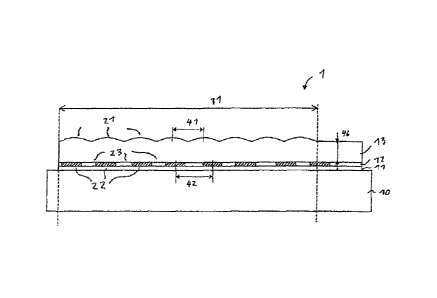
Figure la shows a multilayer body 1 comprising a
carrier substrate 10 and a film element applied on the
carrier substrate, comprising an adhesive layer 11, a
decorative layer 12 and a transparent layer 13.
The carrier substrate 10 is preferably a paper
substrate having a layer thickness of between 10 gm and
200 pm. If the multilayer body 1 is a packaging, then
the carrier substrate can also be a (thick) cardboard
or plastic substrate. However, it is also possible for
the carrier substrate 10 to be a substrate comprising
one or a plurality of layers. The carrier substrate 10
preferably forms the carrier substrate of a valuable
document, preferably of a banknote, and is thus, for
example, optionally also printed with one or a
plurality of layers on the front side and/or on the
rear side.
CA 02772149 2012-02-24
19
The film element comprising the layers 11, 12 and 13 is
applied in the form of a patch or strip onto the
carrier substrate 10. Said film element is thus, for
example, a security thread or security strip, in
particular a window security thread or window security
strip. However, it is also possible for the film
element to cover the entire region of the carrier
substrate 10 over the whole area. The film element
comprising the layers 11, 12 and 13 is preferably
applied as a transfer layer of a transfer film, in
particular of a hot embossing film, onto the substrate
10. However, it is also possible for the film element
to be embodied as a laminating film or as a security
thread and to be applied as such onto the carrier
substrate 10 or to be introduced into the carrier
substrate 10.
The layer 11 is an adhesive layer having a layer
thickness of between 0.5 and 10 gm, preferably between
1 and 5 gm.
The decorative layer 12 is a layer having a
multiplicity of microimages 22 arranged in accordance
with a microimage grid. The decorative layer 12 thus
consists, for example, of a structured, partially
provided metal layer, in particular a metal layer
having a layer thickness of 10 nm to 5000 nm, which is
shaped regionally in patterned fashion in order to form
the microimages 22. In this case, the microimages 22 in
each case show a motif formed by the contrast between
one or a plurality of image regions and one or a
plurality of background regions 23 which exhibit a
different optical appearance. Thus, in the
configuration of the decorative layer 12, as explained
above, as a partial metal layer, by way of example, the
metal of the metal layer is provided in the image
regions and not provided in the background regions 23,
CA 02772149 2012-02-24
such that the microimages 22 are manifested by the
contrast between image regions and background regions
23. If the background regions are embodied in
transparent or translucent fashion, for example by
5 means of a transparent or translucent lacquer, the
adhesive layer 11 is visible through the background
regions 23, said adhesive layer thereby serving as a
contrasting background plane with respect to the image
regions. In this case, it has proved to be advantageous
10 to color the adhesive layer 11 with colored pigments
and/or dyes in order thus also to be able to make the
background regions 23 colored. Highly contrasting
motifs composed of, for example, metallic image regions
and colored background regions can thus be obtained. It
15 is likewise possible to color the adhesive layer 11
alternatively or additionally with UV-active or IR-
active pigments and/or dyes in order to be able to vary
the contrast effect between image regions and
background regions 23 depending on the illumination
20 condition.
Furthermore, it is also possible for the microimages 22
to be formed not only by the decorative layer 12 but by
a decorative layer printed directly on the carrier
substrate 10 and/or by the superimposition of the
decorative layer 12 with such a layer applied directly
to the carrier substrate 10. It is thus possible, for
example, to print on features which have a small phase
variation with respect to the grid of the microlens
grid. Furthermore, by way of example, an offset
printing can have a grid of background colors and image
colors which has a frequency spread, whereas the lens
grid has a constant frequency.
Instead of an offset printing, it is also possible here
to use a different printing method, for example a
gravure printing method, a screen printing method, a
CA 02772149 2012-02-24
21
pad printing method, an intaglio printing method or
else an inkjet printing method.
Furthermore, it is also possible for the layer 12 to be
formed by a colored lacquer layer or a colored
photoresist layer or to consist of a plurality of
(colored) lacquer layers, photoresist layers and/or
metal layers which bring about a different optical
appearance of the decorative layer 12 in the image
regions and background regions and thus form the
microimages 22 in the decorative layer 12. Furthermore,
it is possible for the decorative layer to have a
replication lacquer layer, in which an optically active
surface relief is impressed. In this case, the optical
contrast between image regions and background regions
can be brought about by virtue of the fact that the
surface reliefs are impressed either in the image
regions or in the background regions or, in the image
regions and in the background regions, different
surface reliefs are impressed into the replication
lacquer layer. The replication lacquer layers and, in
particular, the surfaces of the replication lacquer
layers into the which the respective surface relief is
impressed are provided with a reflection-increasing
layer, for example an HRI layer or a metallic layer,
preferably composed of aluminum, silver, copper, gold,
chromium or an alloy comprising such metals. In this
case, the decorative layer 12 thus has a replication
lacquer layer having an impressed surface relief and a
reflection layer, which is preferably arranged below
the replication lacquer layer. In this case, the
optically active surface relief used is preferably a
diffractive relief structure having a spatial frequency
of more than 300 lines/mm, preferably of 500 to
4500 lines/mm. The diffractive relief structure is
preferably a computer-generated diffraction grating,
for example a dot matrix or e-beam hologram, wherein
said diffraction grating differs for example in terms
CA 02772149 2016-10-03
22
of azimuth angle, spatial frequency, profile form or
relief depth in the image regions and background
regions. Furthermore, it is also possible for the
surface relief used to be an anisotropic or isotropic
matt structure, moth-eye structures, asymmetrical or
symmetrical grating structures, linear grating
structures, cross grating structures, hexagonal grating
structures, zeroth-order diffraction structures or
combinations of such diffraction structures.
Furthermore, it is also possible for the decorative
layer 12 to comprise, in addition to or instead of the
abovementioned layer, a thin-film layer system for
producing viewing angle-dependent color shift effects,
a liquid crystal layer or a layer comprising optically
active pigments, for example UV pigments, liquid
crystal pigments or interference layer pigments. This
layer, too, is preferably structured such that it is
provided either in the background regions or in the
image regions and thus brings about a contrast between
image regions and background regions. Furthermore, it
is also possible for the microimages to have a color
profile or different brightness values in the region of
an image region and the corresponding layers of the
decorative layer correspond are configured in order to
correspondingly realize this brightness or color
profile.
The microimages 22 are arranged - as already mentioned
above - in accordance with a one- or two-dimensional
microimage grid, wherein the grid pitch of the
microimage grid, that is to say the respective spacing-
apart of adjacent microimages 22, can be constant or
else can vary. Figure la depicts by way of example a
grid pitch 42 of the microimage grid which is
determined by the microimage distance between the
adjacent microimages 22 shown in figure la, that is to
CA 02772149 2012-02-24
23
say the spacing-apart of the area centroids thereof
with respect to one another.
The layer 13 consists of a material transparent to the
human observer and preferably has a layer thickness of
between 5 and 150 pm. Microlenses 21 are impressed into
that surface of the layer 13 which faces away from the
layer 12, as is indicated in figure la. The microlenses
can be spherical microlenses, but also any other lens
forms, in particular also cylindrical lenses. In this
case, the cylindrical lenses can be embodied
spherically, aspherically or as diffractive lenses
having any desired phase functions. In the simplest
case, the focal length of the lenses is determined here
by their radius of curvature. The focal length of the
microlenses is preferably chosen here such that the
spacing-apart 46 of the microimages 22 from the
microlenses 21 is approximately in the range of the
focal length of the microlenses 21.
The relief depth, that is to say the distance between
the highest and the deepest points of the microlenses,
is in this case preferably between 2 and 50 gm. The
microlenses 21 can be introduced into the surface of
the layer 13 for example by means of an embossing tool,
for example by means of a mechanically acting embossing
roller or an embossing stamp or by means of laser
ablation. In this case, the transparent layer 13
consists for example of a lacquer layer, of a plastic
film, for example a film composed of PET (polyethylene
terephthalate), PEN (polyethylene naphthalate), or BOPP
(biaxially oriented polypropylene) or of a plurality of
layer plies, for example a replication lacquer layer
and a transparent carrier film, for example a PET film,
arranged below the latter. The impression of the
microlenses into the transparent layer 13 is in this
case preferably effected by means of IN replication,
that is to say by impressing the microlens structure
CA 02772149 2017-02-17
24
into a soft, not yet or only slightly cured replication
lacquer layer and subsequently curing the replication
lacquer layer using high-energy radiation, preferably
UV radiation. However, it is also possible that, in
order to produce the microlenses 21, a lacquer is
applied to a transparent layer and is correspondingly
provided with a surface corresponding to the microlens
grid for example by means of a shaping tool or a
physical process. Furthermore, it is also possible for
the microlenses 21 to be diffractive lenses.
Furthermore, it is also possible for even further
transparent layers to be provided in the multilayer
body 1 between the layers 12 and 13, or else for even
further layers to be provided between the layer 11 and
the layer 12 or above the layer 13 in the multilayer
body 1.
The microlenses 21 are arranged - as already explained
above - in accordance with a one- or two-dimensional
lens grid, wherein the grid pitch of the lens grid can
be constant or else can vary locally. Thus, figure la
shows by way of example a grid pitch 41 corresponding
to the microlens distance between the adjacent
microlenses shown in figure la, that is to say the
spacing-apart of the area centroid thereof.
The spacing-apart 46 of the microlenses 21 from the
microimages 22 is preferably approximately in the range
of the focal length of the microlenses 21 and
preferably deviates by not more than 10% from the focal
length of the microlenses 21.
The grid pitch of the microlens grid along the sectional
line of the section shown in figure la in this case is
preferably between 5 and 300 gm and the grid pitch of
the microimage grid in the direction of the sectional
line is preferably between 5 and 300 gm. With
CA 02772149 2012-02-24
regard to the shaping of the microimages 22, the
configuration of the grid pitch of the microimage grid
and microlens grid and the mutual orientation of the
microlens grid and microimage grid, reference is made
5 to the previous explanations.
Preferably, the microlenses 21 are arranged in
accordance with a one-dimensional lens grid, as will be
explained below by way of example with reference to the
10 figures in figure lb to le.
Thus, figure lb shows a plan view of an excerpt from
the layer 13, wherein the focal point lines of the
microlenses 21 shaped in the form of cylindrical lenses
15 is indicated by lines in figure lb. The microlenses 21
are arranged in accordance with a one-dimensional
microlens grid which spans a coordinate system having
the axes 50 and 51. The axis 50 of the coordinate
system is oriented parallel to the transverse axis of
20 the multilayer body 1 and parallel to the focal point
lines of the microlenses 21 and the coordinate axis 51
is oriented perpendicular to the coordinate axis 50. In
this case, the microlenses 21 preferably have a length
of more than 1 mm and the distance between adjacent
25 microlenses 21, the grid pitch 41, is less than 300 lam,
preferably between 10 and 200 pm. In the embodiment in
accordance with figure lb, the area centroid lines of
the microimages 22 are preferably oriented
substantially parallel or parallel to the coordinate
axis 50 and the grid pitches of the microimage grid and
of the microlens grid differ from one another, in
particular by between 0.5 and 596-.
A further preferred exemplary embodiment will now be
explained with reference to the figures in figure lc
and figure Id.
CA 02772149 2016-10-03
26
Figure lc shows a plan view of the layer 13, wherein -
as in figure lb - the focal point lines of the
microlenses 21 are identified by corresponding lines.
Here, too, the microlenses 21 are formed by cylindrical
lenses arranged in accordance with a one-dimensional
microlens grid having a grid pitch 41 of between 10 pm
and 300 gm, here 35 gm. The focal length of the
microlenses is between 10 gm and 500 Rm. As shown in
figure id, the focal point lines of the microlenses 21
are in this case rotated at an angle of 45 relative to
the longitudinal axis of the multilayer body 1 and are
arranged substantially parallel to one another. In this
case, the coordinate axis 51 illustrates the
longitudinal direction of the multilayer body 1 and the
coordinate axis 50 the transverse direction of the
multilayer body 1, which is preferably a strip-shaped
or thread-shaped security element. As explained in
figure lb, the microimages 22 are arranged in
accordance with a microimage grid, which - as described
above - is arranged in a manner rotated relative to the
microlens grid (in particular is rotated by 45 ) or, as
described above, differs therefrom in terms of the grid
pitch. This results in the optical appearance 60
illustrated in figure ld, in the case of which optical
appearance foreground elements 61 describe a left-right
movement upon the tilting of the multilayer body 1 into
the horizontal axis and a left-right movement upon the
tilting of the multilayer body 1 about the vertical
axis.
In the exemplary embodiment according to figure id, the
multilayer body 1 has, by way of example, a length of
100 mm and a width of 10 mm, that is to say a
longitudinal dimension of 100 mm and transverse
dimension of 10 mm.
A further embodiment is illustrated by figure le.
Figure le likewise shows a plan view of the layer 13,
CA 02772149 2016-10-03
27
wherein the focal point lines of the microlenses 21 are
likewise indicated here by lines. In this case, the
microlenses 21 are formed by cylindrical lenses which
are arranged concentrically with respect to one another
and which each have a circular shaping and are arranged
in a manner spaced apart from one another in a grid
pitch 41 - as indicated in figure le. Furthermore, it
is also possible for the microlenses 21 to be arranged
in accordance with a geometrically transformed one-
dimensional microlens grid and thus, by way of example,
for the focal point lines of the microlenses in the
plane spanned by the coordinate axes 50 and 51 in each
case to have a wavy-line shaping.
A further exemplary embodiment is illustrated with
reference to figure if. Figure if shows an excerpt from
the multilayer body 1 with a microlens 21 and an
assigned microimage 22. The microlens 21 is a
cylindrical lens having a radius 47 and a maximum
structure height 44. In the exemplary embodiment
according to figure if, the
microimages 22 - in
contrast to what is shown in figure la - are not
arranged in a planar plane, but rather are arranged on
a surface of the layer 13 which is curved in the region
of the respective microimage 22. For this purpose, a
surface structure is replicated into the layer 13 both
into the top side and into the underside, wherein the
surface structures provided in the region of the
microimages 22 preferably has a lens-type shaping - as
has been illustrated in figure if. As already explained
above, the microstructure impressed into the layer 13
in the region of the microimages 22 has a similar
shaping to the microlens 21 and thus forms a curvature
in the form of a cutout of a cylindrical surface, as is
illustrated in figure if.
CA 02772149 2012-02-24
28
In the case present here, in which the microlens 21 is
embodied as a spherical cylindrical lens having a
radius 47, the following approximately holds true:
1 Hh 0.074
xi 3r
In this case, r is the radius of the microlens 21 and xi
is the position of the image with respect to the normal
to the surface of the layer 13, that is to say
corresponds to the dimension 46. For a radius
r = 50 pm, this results in a parallax focus of 150 pm
and a value of 122.75 pm for the outermost image edge,
that is to say a deviation of 18%. The curvature for
the microimage 22 is accordingly to be chosen such that
the deepest location of the microimage 22 is at a
distance of 150 pm from the top side facing away from
the microimage, that is to say that the dimension 46 is
150 pm, and that in the edge region of the image the
microimage is arranged at a distance of 122.75 pm from
the top side layer 13.
Figure 2 shows a multilayer body 2, which is improved
and modified relative to the multilayer body 1 in the
manner described below:
The multilayer body 2 comprises the carrier substrate
10 and the film element comprising the layers 11, 12
and 13. The layer 13 is embodied like the layer 13
according to figure la to figure if with the difference
that the microlenses 21 in the region 31, unlike in the
case of the embodiment according to figure 1, do not
directly succeed one another, rather that "flat"
regions are provided between the microlenses 21, which
regions are not part of a microlens and do not
contribute anything to the deflection function of the
microlenses 21. As illustrated in figure 2, the lenses
have, in the direction of the sectional line of the
CA 02772149 2016-10-03
29
section illustrated in figure 2, a dimension 43 which
is smaller than the respective grid pitch of the
microlens grid along the sectional line by at least
30%, in particular by more than 50%, that is to say
that the dimension 43 is 5 0.5 grid pitch 41.
Furthermore, the microlenses 21 have a maximum
structure height, that is to say dimension 44, which is
at least 25%, in particular at least 50%, of the
dimension 43 of the microlenses. This configuration of
the microlenses makes it possible to correspondingly
reduce the layer thickness of the layer 13 and - as
illustrated in figure 2 - to make the layer thickness
of the multilayer body 2 significantly smaller than the
layer thickness of the multilayer body 1. As already
mentioned above with regard to figure la, the distance
between the base point plane of the microlenses 21 and
the decorative layer 12 is in this case chosen
approximately (deviation 10%) such that it
corresponds to the focal length of the microlenses 21.
Since the microlenses 21, on the other hand, cover a
significantly smaller proportion of the area of the
region 31, the maximum structure height of the
microlenses 21 also correspondingly decreases upon the
reduction of the focal length of the microlenses 21,
such that a particularly thin configuration of the
multilayer body 2 can be obtained by means of these two
effects.
The decorative layer 12 is embodied like the decorative
layer 12 according to figure la, wherein figure 2 shows
an embodiment of the multilayer body 2 in which the
decorative layer consists of a transparent replication
lacquer layer 122 and a whole-area metal layer 121,
wherein, in the regions forming the image regions of
the microimages 22, a diffractive relief structure 123
is impressed into the surface of the replication
lacquer layer 122 and such a relief structure is not
impressed into the background regions
CA 02772149 2012-02-24
23, that is to say that these regions are embodied as
mirror regions. It is also worth mentioning here,
moreover, that in the embodiment according to figure 2
the dimension 45 of the microimages 21 in a first
5 spatial direction, here in the direction of the
sectional line of the section shown in figure 2, is
more than 50%, in particular more than 100%, of the
dimension 43 of respectively adjacent microlenses 21 in
the first spatial direction. The advantages already set
10 out above are obtained as a result.
In the case of the exemplary embodiment shown in
figure 2, the dimension 43 is preferably between 5 pm
and 100 pm, the maximum structure height 44 of the
15 microlenses 21 is between 3 pm and 50 pm, and the
dimension 45 of the microimages 22 is preferably
between 3 pm and 50 pm. With regard to the other
configurations of the multilayer body 2, reference is
made to the explanations concerning the multilayer body
20 1 according to figure la to figure if.
Figure 3 shows a multilayer body 3 constituting a
banknote. The multilayer body 3 has in the region 31
the carrier layer 10, the adhesive layer 11, the
25 decorative layer 12 with the microimages 22 and the
transparent layer 13 with the microlenses 21. In this
case, the transparent layer 13 can be linked integrally
with the carrier layer 10, that is to say that the
microlenses 21 can also be introduced, preferably
30 embossed, directly as surface relief into the carrier
layer 10 without the use of a separate layer 13. If a
separate layer 13 is applied to the carrier layer 10,
this can advantageously be a radiation-curing lacquer,
into which the microlenses 21 are embossed by means of
an embossing roller and the lacquer is subsequently
cured e.g. using UV radiation. With regard to the
configuration of these layers, reference is made to the
above explanations according to figure la to figure 2.
CA 02772149 2012-02-24
31
The carrier substrate 10 is the carrier substrate of
the banknote. In a region 32, the carrier substrate 10
is embodied in transparent fashion. If the carrier
substrate 10 consists, for example, of a plastic film
or of a multilayered laminate of a plurality of plastic
layers, then these plastic layers are embodied such
that they are transparent to the human observer in the
region 32. If a paper substrate is involved, then the
carrier substrate 10 preferably has in the region 32 a
window-shaped perforation, which is then covered on
both sides by the layers shown in figure 3. Outside the
region 32, the carrier substrate 10 is preferably
embodied in opaque fashion, that is to say printed with
corresponding opaque layers or provided with a
correspondingly colored layer. Onto the carrier
substrate 10, a film element comprising the layers 11
and 13 is then applied onto the front side and a film
element comprising the layers 11, 12 and a layer 15 is
applied onto the rear side. The layer 15 is an optional
protective lacquer layer. The application of these film
elements onto the carrier substrate 10 can be carried
out by means of one of the methods described above, for
example by means of transferring the transfer layer of
a transfer film or laminating a laminating film onto
the carrier substrate 10.
As illustrated in figure 3, the film elements applied
on the carrier substrate 10 are in this case made
particularly thin, since the carrier substrate here is
advantageously used as an additional spacer layer for
foLming the first optically variable effect and,
consequently, the layer thickness of the layer 13 can
be chosen to be particularly thin.
Furthermore, it is also possible here for the
decorative layer 12 not to be part of a film element
applied onto the carrier substrate 10, rather for the
CA 02772149 2012-02-24
32
decorative layer 12 to be applied directly to the
carrier substrate 10 by means of a printing method.
The advantages already described above are obtained by
means of the multilayer body 3.
Figure 4 shows a multilayer body 4 constituting a
modification of the multilayer body 3 according to
figure 3. The multilayer body 4 comprises the carrier
substrate 10, the adhesive layers 11, the decorative
layer 12 with the microimages 22, the transparent layer
13 with the microlenses 21, and the protective lacquer
layer 15. The multilayer body 4 is configured like the
multilayer body 3 according to figure 3 with the
difference that the carrier substrate 10 is embodied in
completely transparent fashion, and that a replication
lacquer layer 14 is arranged above the transparent
layer 13, the refractive index of said replication
lacquer layer differing from the refractive index of
the material of the layer 13. The film element applied
to the front side of the carrier substrate 10 is in
this case preferably produced as follows:
The replication lacquer layer 14 is applied to an
optional carrier layer and release layer (in the case
of a transfer film) and a surface relief corresponding
to the microlens grid with the microlenses 21 is
embossed into the replication lacquer layer 14.
Afterward, said surface relief is filled with a further
lacquer layer, the layer 13, and the further layers, in
particular the adhesive layer 11, are then applied.
Afterward, the film element is applied onto the carrier
substrate 10. The embodiment according to figure 4 here
has the further advantage that the surface structure of
the microlenses 21 is not impressed in the front side,
that is to say the upper surface, of the multilayer
body and therefore cannot be reproduced by means of a
contact copy. Furthermore, the microlenses are thus
CA 02772149 2016-10-03
-
33
protected against mechanical wear, for example
scratches, by the layer 14, such that the durability of
the multilayer body is improved.
Figure 5 shows a multilayer body 5 constituting a
further variation of the multilayer body 3 and of the
multilayer body 4 according to figure 3 and figure 4,
respectively. The multilayer body 5 comprises the
carrier substrate 10, the layer 11, the decorative
layer 12 with the microimages 22, the layer 13 with the
microlenses 21, and the layer 14. The multilayer body 5
is embodied like the multilayer body 4 according to
figure 4 with the difference that the film element
applied onto the front side of the carrier substrate 10
furthermore has a security element 16, the film element
applied onto the underside of the carrier substrate has
a security element 18 and a cover layer 17, and the
underside of the carrier substrate 10 is provided with
an imprint 19.
The cover layer 17 is formed by an opaque layer which
decouples the optical effect of the decorative layer 12
and the optical effect of the security element 18 from
one another. This layer could also be dispensed with.
The security elements 16 and 18 each consist of one or
a plurality of layers, selected from the group
comprising replication lacquer layer with impressed
optically active surface relief, reflection layer,
metal layer, color lacquer layer, layer comprising
optically active pigments, liquid crystal layer, volume
hologram layer and thin-film layer system. In this
case, the security element 18 preferably forms a second
optically variable information item, which differs from
the first optically variable information item generated
in the region 31 by the layers 13, 15 and 12. Upon
viewing from the front side, the optically variable
effect generated by the layers 12 and 13 is thus
visible in the region 31 and, upon viewing from the
CA 02772149 2012-02-24
34
rear side, the optically variable effect generated by
the security element 18 is visible.
The security element 16 can be configured like the
security element 18. The security element 16 thus
generates a corresponding, preferably optically
variable impression in a region 33, in which it is
provided in the film element applied with the front
side of the carrier substrate 10, upon viewing from the
front side. Furthermore, the security feature 16 is
arranged with register accuracy with respect to the
security element 18. Upon transmitted-light viewing,
the security elements 16 and 18 complement one another
to form a further security element, for example form
mutually complementary representations which combine to
form an overall motif, for example, upon transmitted-
light viewing. Part of said overall motif is
furthermore the imprint 19, which is likewise arranged
with register accuracy with respect to the security
elements 16 and 18. Upon viewing from the front and
rear sides in reflected light, preferably the optically
variable effect generated by the security element 16 is
thus manifested in the region 33 and, upon viewing in
transmitted light, the "watermark effect" provided by
the imprint 19, the security element 16 and the
security element 18 is manifested in the regions 31, 33
and 34, said "watermark effect" being determined by the
register-accurate arrangement of the layers of the
security elements 16 and 18 and of the imprint 19 with
respect to one another.
Figure 6 shows a multilayer body 6 comprising the
carrier substrate 10, the adhesive layer 11, the
decorative layer 12 with the microimages 22 arranged in
the region 31, and the transparent layer 13 with the
microlenses 21 arranged in the region 31. The
abovementioned layers are embodied like the
correspondingly designated layers of the multilayer
CA 02772149 2012-02-24
body 1 and 2 according to figure la to figure 2 with
the difference that, in the region 31, a window-shaped
perforation is additionally provided in the carrier
substrate 10. With regard to the configuration of these
5 layers, reference is thus made to the explanations
above. Furthermore, a translucent layer 20 is arranged
between the decorative layer 12 and the transparent
layer 13. The translucent layer 20 preferably consists
of a colored lacquer layer and preferably has a layer
10 thickness of between 1 pm and 30 pm.
Furthermore, the decorative layer is embodied such that
the transparency of the decorative layer is different
in the image regions and in the background regions; by
15 way of example, the background regions are configured
in fully transparent fashion and the image regions are
configured in opaque fashion.
What is achieved by the above-described configuration
20 of the multilayer body 6 is that the optically variable
effect generated in the region 31 by the layers 12 and
13 is manifested only in transmitted-light viewing and
is extinguished in reflected-light viewing by the
translucent layer 20 and the scattering effect brought
25 about by the latter.
Figure 7 shows a multilayer body 7 comprising the
carrier substrate 10, the adhesive layer 11, the
decorative layer 12 and the transparent layer 13. These
30 layers are embodied like the correspondingly designated
layers according to figure la to figure 2, apart from
the following differences:
The decorative layer 12 has zones 34 and 33 in the
35 region 31. In the zones 33, the decorative layer 12 is
configured in the manner described above with respect
to figure 1 or figure 2. In the zones 33, the
decorative layer 12 has a replication lacquer layer
CA 02772149 2012-02-24
36
having an optically active surface structure 24, which
is provided for generating a further optically variable
information item, which differs from the first
optically variable information item generated in the
zones 34. Furthermore, in the zones 33, a lacquer layer
30 is printed onto the surface of the transparent layer
13. The lacquer layer 30 is a lacquer layer composed of
a material whose refractive index differs from the
refractive index of the material of the transparent
layer by not more than 0.3. This has the effect that
the optical effect of the microlenses 21 is
extinguished in the zones 33 for the human observer and
only the optically variable effect generated by the
optically active surface structure 24 thus becomes
visible in the zones 33 for the human observer.
A further variant for obtaining the optical effect
generated by the multilayer body 7 is explained below
with reference to figure 8.
Figure 8 shows a multilayer body 8, comprising the
carrier substrate 10, the adhesive layer 11, the
decorative layer 12 and the transparent layer 13. These
layers are constructed like the correspondingly
designated layers according to figure 7 apart from the
following differences: instead of extinguishing the
optical effect of the microlenses 21 in the zones 33,
here firstly the variant is shown where the layer 13 is
not provided in the region of the zones 33. The layer
13 is thus fashioned partially, such that the layer 13
with the microlenses 21 is not provided in the zones 33
or in a portion of the zones 33. As a result, the
optically variable effect of the optically active
surface structures 24 is manifested particularly
brilliantly in these regions 33 because there is no or
only partial covering of the optically variable effect
by other layers. As an alternative thereto, it is
possible for the microlenses to be impressed only
CA 02772149 2012-02-24
37
partially into the layer 13. As shown in figure 8, the
microlenses are thus not impressed in the zones 33 and,
by way of example, as shown in figure 8, are replaced
by a planar surface profile or a substantially smooth
or planar surface profile without an optical distortion
function.
Alternatively, investigations have shown that even when
dispensing with the lacquer layer 30 or when
implementing one of the two preceding measures, the
optical impression of the surface structure,
particularly when a Kinegram is used, is only slightly
blurred by the lenses and it is thus possible, if
appropriate, to dispense with the lacquer layer 30 or
one of the two abovementioned alternatives thereto for
obtaining the optically variable effect outlined in the
exemplary embodiment according to figure 7.
It is furthermore possible that as zones 34 regions
having differently embodied and/or oriented microimage
grid and microstructure grid, as illustrated previously
in figures lb, lc, id, le, and zones 33 for generating
a further optically variable information item are
arranged adjacent to one another alongside one another.
Adjacent in this context means that zones respectively
lying alongside one another have a common boundary line
or boundary zone. In order to be able to compensate for
the presence of manufacturing tolerances of the
positions of the respective zones, it is possible for
zones respectively lying alongside one another to
slightly overlap one another in an overlap region
embodied as a boundary zone, wherein the boundary zone
is in each case preferably slightly wider than the
maximum manufacturing tolerance, for example has a
width of between 10 jtm and 5 mm. Boundary zones can be
provided at the entire periphery of a zone or only at
part of the periphery, for example only in the region
CA 02772149 2012-02-24
38
of a boundary line with respect to an adjacent zone.
Such manufacturing tolerances can occur for example
when applying the individual layers in different
production steps, preferably in a roll-to-roll process
for the microimage grids and/or of the microstructure
grids, as a result of which a small offset in the
relative arrangement of the layers with respect to one
another can arise.
Figure 9 shows a multilayer body 9 comprising the
regions 35, 36 and regions 37 and 38. In the regions 35
to 38, the microimage grid and the microstructure grid
respectively differ from one another, in particular in
one of the parameters selected from the group
comprising microimage distance, microstructure distance
and orientation of the coordinate axis which are
spanned by the microstructure grid and the microimage
grid. The microimage grid or the microstructure grid
can also be identical in individual regions 35 to 38,
but phase-shifted relative to the respective other
regions. In the regions 37 and 38, by way of example,
the zones 21, 22 and 23 are thus arranged in accordance
with a microstructure grid and a microimage grid, in
which the difference between the microimage distance
and the microstructure distance is positive in the
region 134 and negative in the region 135. By way of
example, this brings about a contrary movement of the
motif manifested during tilting in the regions 37 and
38.
In addition, an advantageous combination of zones 34
having optically variable information items with
adjacent zones 33 having an optically variable
information item contrasting therewith is possible, for
example as individual motifs within an overall motif,
in order that the zones 33 can serve as a contrasting
optical reference to the optically variable information
item in the zones 34. By way of example, there can be
CA 02772149 2012-02-24
39
movement effects in the regions 35 to 38 and a
surrounding region 39 without a movement effect or a
movement effect in the region 38 with a region 37
surrounding or adjoining the latter without a movement
effect, for example with a hologram and/or with
optically variable pigments or else in each case
contrary movement effects in the regions 35 to 38.
Contrasting optically variable information items can
also be generated, for example, by virtue of the fact
that, in one or a plurality of regions 35 to 38, a
microstructure grid is provided above a microimage grid
or above other optically variable motifs and, in other
regions 35 to 38 directly or indirectly adjacent
thereto, the microstructure grid is either
extinguished, for example by means of a lacquer layer
having a similar refractive index, or is not provided.
It is likewise possible to provide in the regions 35 to
38 optically variable information items adjacent with
optically static information items, for example single-
colored regions or multicolored, non-optically variable
motifs, adjacent to one another.