Note: Descriptions are shown in the official language in which they were submitted.
CA 02772397 2012-03-22
Resonant circuit inverter with controllable operat g point
BACKGROUND OF THE INVENTION
(1) Field of the Invention
The present invention relates to a resonant circuit inverter with a
controllable
operating point.
(2) Description of Related Art
Resonant circuit inverters are described, for example, in the textbook
"Leistungselektronik" (Power Electronics) by Rainer Felderhoff, published by
Carl
Hanser Verlag, 2"d edition, ISBN 3-446-18993-9. The resonant circuit inverters
described therein have, for example, a three-phase rectifier, a DC-link
circuit and
a single-phase inverter, with the output of the inverter forming the output of
the
resonant circuit inverter through which the current flows to the connected
load.
Resonant circuit inverters are frequently used as frequency converters.
The document EP 0 617 503 Al describes a method and an apparatus for
controlling the operating point of a resonant circuit inverter. The resonant
circuit
inverter disclosed in this document is used for inductive heating of a heated
material. The document describes the significance of the frequency of the
current
in the load circuit selected for inductive heating. The frequency of the
output
current is advantageously either slightly greater than the resonance frequency
or
slightly smaller than the resonance frequency, depending on the selection
and/or
availability of the electro-technical components. As also described in the
document, the load circuit then assumes an inductive characteristic or a
capacitive characteristic, which means that the output current is either
lagging or
leading the voltage at the output of the resonant circuit inverter. The
operating
point for operating the resonant circuit inverter described in the document is
determined by the phase angle between the output current and the voltage at
the
output of the resonant circuit inverter.
1
CA 02772397 2012-03-22
In the aforedescribed inductive heating application, the parameter in the load
circuit changes due to the heating, causing the resonance frequency to change.
The phase angle between the output current and the voltage at the output of
the
resonant circuit inverter also changes, i.e., the operating point changes,
which is
undesirable.
It was an object of the solution described in the aforementioned document to
propose a method and an apparatus for controlling the operating point of a
series
resonance circuit inverter, so that the predetermined operating range for the
resonant circuit inverter can be identified and kept stable independent of
parameter variations of the oscillating circuit elements.
The aforementioned document discloses a control of the phase angle, wherein
the controller evaluates the difference between a nominal phase angle and an
actual phase angle and depending on the evaluation adjusts the frequency of
the
output current by operating on the inverter. The phase angle may be, for
example, the angle between the output current and the voltage at the output of
the inverter.
The document also describes using the phase angle between other quantities,
because using particularly the output current may sometimes be
disadvantageous.
A resonance circuit inverter can not only be used to inductively heat
materials.
Materials may also be heated by conducting current through the materials and
using their effective resistance, as is the case, for example, when heating
silicon
rods or thin silicon rods in the manufacture of polysilicon by chemical vapor
deposition with the Siemens process.
2
CA 02772397 2012-03-22
As in inductive heating of materials, when heating silicon rods or thin
silicon rods
(also referred to as silicon seed rods), the growth of the silicon rods or
thin silicon
rods changes parameters in the oscillating circuit. The resonance frequency of
the oscillating circuit then also changes with chemical vapor deposition,
requiring
an adjustment of the operating point commensurate with this change. The
operating point can be adjusted in vapor deposition as well as in inductive
heating by changing the phase angle between the output current and the voltage
at the output of the resonant circuit inverter.
Double-commutations may occur in a resonant circuit inverter, in particular
when
using a single phase inverter with H-connection, at frequencies close to the
resonance frequency, which causes in short succession directional changes in
the output current. These multiple directional changes result in several zero
crossings of the output current, making detection of a zero crossing for
detecting
the phase angle between the output current and the voltage at the output of
the
resonant circuit inverter at least difficult.
This is a starting point for the invention.
BRIEF SUMMARY OF THE INVENTION
It is an object of the invention to propose a resonant circuit inverter which
allows
a control of the phase angle, i.e., of the operating point, without requiring
detecting the zero crossing of the output voltage.
This object is attained with the invention in that for determining the actual
phase
angle, wherein a difference can be determined between
- a measured time which can be measured between a time when a turn-on
pulse is applied to a control electrodes of a controllable switch of the
inverter receiving the output current and the time of the subsequent zero
crossing of the output current, and
3
CA 02772397 2012-03-22
a known dead time between the time when a turn-on pulse is applied to a
terminal of the inverter for receiving the output current by a controllable
switch of the inverter and a subsequent reversal of the voltage at the
output of the inverter.
At a known frequency, the phase angle between the times of the end of the dead
time and the zero crossing of the output current within one period of the
output
current and/or the output voltage can be determined from this difference,
without
creating a problem for a skilled artisan.
A resonant circuit inverter according to the invention may include a second
control means for controlling the output current. If the output current
provided by
the resonant circuit inverter is not sufficient even when the phase angle is
properly controlled, then the output current can be controlled, so that the
actual
output current can reach a desired nominal output current. Advantageously,
control of the output current is here slower than control of the phase angle,
so
that the resonant circuit inverter is always operated at the desired operating
point
and with the output current resulting at the desired operating point.
A means for forming a control difference from a signal for a nominal output
current and a signal for an actual output current measured with a current
sensor
may be associated with the second control means. The resonant circuit inverter
may include a means for forming the absolute value of the control difference
and
for comparing the absolute value of the control difference with a
predetermined
value. Depending on a result of this comparison, either only the first control
means for controlling the phase angle may be activatable or deactivatable, or
both the first control means for controlling the phase angle and the second
control means for controlling the output current may be activatable or
deactivatable.
4
CA 02772397 2012-03-22
For a small control deviation of the output current, the intent is to achieve
the
desired current by first controlling the phase angle, i.e., the operating
point. This
is particularly useful if the control difference between the actual phase
angle and
the nominal phase angle is large and the frequency adjusted at the inverter is
significantly different from the resonance frequency. In this case, one can
assume that a substantially larger current may be attained at the operating
point
with the desired nominal phase angle than with the adjusted frequency.
Control of the output current is activated only if this is not sufficient or
if the
magnitude of the control deviation is too large. A control value for the DC
voltage
in the DC-link circuit is then supplied to the rectifier. The rectifier can
adjust
(preferably control) this voltage in the DC-link circuit. Because the output
current
depends directly from the DC-link voltage, the output current can be
controlled by
changing the DC-link voltage.
When operating a resonant circuit inverter according to the invention, the
resonance frequency can be initially determined for initializing the resonant
circuit
inverter. The resonance frequency can be determined by decreasing the
frequency, starting from a start value, and then measuring the output current.
The frequency where the largest output current is measured can then be
determined as the resonance frequency. Because no reactive current is present
in the output circuit, the highest effective current is measured at resonance.
The
resonance frequency can thus be determined in practice by measuring the output
current.
After the resonance frequency is determined, the phase angle can be controlled
with the first control means for the phase angles. For controlling the phase
angle,
the difference can be determined between
- a measured time which can measured between a time when a turn-on
pulse is applied to a control electrode of a controllable switch of the
CA 02772397 2012-03-22
inverter receiving the output current and the time of the subsequent zero
= crossing of the output current, and
a known dead time between the time when a turn-on pulse is applied to a
control electrode of a controllable switch of the inverter receiving the
output current and a subsequent reversal of the voltage at the output of
the inverter.
The actual phase angle can then be determined from the difference and a
control
difference can be formed from a nominal phase angle and the actual phase
angle. The frequency can be changed with the first control means depending on
the control difference of the nominal phase angle and the actual phase angle
as
a controlled variable for the inverter, so that the nominal phase angle is
adjusted
at the output of the inverter.
After the phase angle is property adjusted, control of the output current with
the
second control means can be started, if a magnitude of a control difference
between the nominal output current and the actual output current is greater
than
a predetermined value.
BRIEF DESCRIPTION OF THE SEVERAL VIEWS OF THE DRAWING(S)
Additional features and advantages of the present invention will now be
described with reference to the drawings, which show in
FIG. 1 a high-level circuit diagram of a circuit arrangement according to the
invention with a resonant circuit inverter according to the invention and
loads connected to the circuit arrangement,
FIG. 2 resonance curves of the resonant circuit inverter and of components
connected thereto,
6
CA 02772397 2012-03-22
FIG. 3 the curve shape of an output voltage of the resonant circuit inverter,
of
an output current of the resonant circuit inverter, of an output current of
the circuit arrangement, and of a control voltage applied on a control
electrode of a rectifier valve of the inverter over slightly more than one
period,
FIG. 4 a detail of FIG. 3, and
FIG. 5 a schematic control circuit diagram of the circuit arrangement
according to the invention.
DETAILED DESCRIPTION OF THE INVENTION
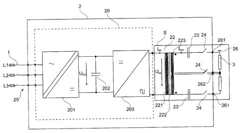
FIG. 1 illustrates only the power-electronic components of the circuit
arrangement according to the invention. Controllers, measurement transducers
or other components or elements required for regulating or controlling the
power-
electronic components are not shown.
The circuit arrangement according to the invention illustrated in FIG. 1 has a
three-phase input 25 with terminals connected with a three-phase network L1,
L2, L3 via switches and fuses 1. The network may be a public low-voltage power
grid. The circuit arrangement according to the invention produces from the
three-
phase AC voltage at the input 25 a 2-phase AC voltage across the output 26 of
the circuit arrangement 2.
The voltages of the two-phase AC voltage are shifted with respect to each
other
by 1800, i.e. by half a period, and thus have opposite phases. Furthermore,
the
voltages of the two-phase AC voltage system have the same effective value. The
voltage between the phase conductors of the two-phase AC voltage system is
therefore zero.
7
CA 02772397 2012-03-22
Each of the outputs 26 has a phase conductor terminal 261 and a center
. = conductor terminal 262. A respective load 3 is connected between the
corresponding phase conductor terminal 261 and a center conductor terminal
262. This load may be, for example, one or several silicon rod pairs in a
Siemens
reactor.
It is the object of the circuit arrangement according to the invention to
produce,
inter alia, the two-phase AC voltage from the three-phase AC voltage.
It is another object of the circuit arrangement 2 according to the invention
to
enable with the circuit arrangement 2 according to the invention an adjustment
of
the frequency of the two-phase AC voltage at the outputs 26.
It is yet another object to be able to enable with the circuit arrangement 2
according to the invention an adjustment of the current through the outputs
26.
For adjusting the frequency of the current and the magnitude of the current
flowing through the outputs 26 of the circuit arrangement 2 according to the
invention, the circuit arrangement 2 according to the invention has a resonant
circuit inverter 20.
The resonant circuit inverter 20 includes as a rectifier a six-pulse bridge
circuit
(B6 circuit), a three-phase AC current transformer connected upstream of the
bridge circuit and enabling galvanic isolation from the network. The six-pulse
bridge circuit includes controllable converter valves, so that the DC voltage
at the
output of the six-pulse bridge circuit can be adjusted. The transformer and
the
six-pulse bridge circuit are indicated in FIG. 1 by a symbol having the
reference
number 201.
In the so-called DC link circuit, a capacitor 202 is connected in parallel
with the
output of the six-pulse bridge circuit, as is known in the art.
8
CA 02772397 2012-03-22
An inverter 203 is connected downstream of the DC link circuit with the
capacitor
202. The inverter 203 is a single-phase inverter with an H-circuit of
converter
valves.
The frequency of the current supplied by the inverter 203 depends on the
switching frequency of the converter valves of the inverter 203. The magnitude
list
of the current supplied by the inverter depends on the DC voltage UDC in the
DC
link circuit, which can be adjusted by way of the six-pulse bridge circuit.
The resonant circuit inverter 20 is essentially known in the art.
A transformer 22 is connected downstream of the resonant circuit inverter 20.
The transformer 22 has a primary winding 221 which is connected to the output
of the inverter 203 or the output of the resonant circuit inverter 20,
respectively.
The transformer 22 moreover has two secondary windings 222, 223. The two
secondary windings 222, 223 are wound in opposite directions and arranged on
a leg of a transformer core of the transformer 22. They are therefore
penetrated
by the same magnetic field.
Adjacent ends of the secondary windings 222, 223 are connected with one
another and form the center point of the two-phase voltage system provided at
the output of the circuit arrangement 2 according to the invention, The center
point is connected with terminals 262 of the outputs 26 of the circuit
arrangement
2 by way of switches 24.
The remaining opposite ends of the secondary windings 222, 223 are each
connected with the terminal 261 of the outputs 26 via a corresponding
capacitor
23 and a switch 24. These terminals form the terminals for the phase
conductors
of the two-phase voltage system provided by the circuit arrangement 2
according
to the invention.
9
CA 02772397 2012-03-22
The transformer 22, the capacitors 23 and the loads 3 form an oscillator
circuit S
at the output of the resonant circuit inverter 20. As any oscillator circuit,
this
oscillator circuit has a resonance frequency.
The effective power converted in the oscillator circuit S is highest when the
frequency of the output current flowing via the output of the resonant circuit
inverter 20 and hence via the oscillator circuit S is equal to the resonance
frequency. The reactive power in the resonance circuit S is then as small as
possible.
It would therefore be desirable to operate the inverter 203 of the resonant
circuit
inverter 20 at the resonance frequency of the oscillator circuit S.
However, it has been observed that it is disadvantageous for several reasons
to
operate the inverter at the resonance frequency of the oscillator circuit. For
example, undesirable double commutations occur during the operation of the
inverter 203.
These can be prevented if the frequency is slightly higher than the resonance
frequency of the oscillator circuit S. If the frequency is slightly higher
than the
resonance frequency, then a phase angle is present between the output current
ljst of the resonant circuit inverter 20 and the output voltage U;St of the
resonant
circuit inverter 20.
This also indicates that the operating point is in an inductive range, so that
the
diodes are not so highly loaded and the dissipated power through the diodes is
not high. The double commutations do not occur.
According to the invention, the operating point for operating the resonant
circuit
inverter 20 is determined by a predetermined phase angle. Once a
CA 02772397 2012-03-22
predetermined phase angle is adjusted, the resonant circuit inverter 20 is
operated at the desired operating point.
Because at least the loads 3 of the oscillator circuit S have a changeable
impedance - these are silicon rods whose resistance changes - the parameter of
the oscillator circuit S change during operation of the circuit arrangement
according to the invention, causing a change in the resonance frequency. For
example, the resonance frequency may increase, as indicated in FIG. 2.
To always maintain the same operating point, the frequency at which the
inverter
203 is operated, must thus be adjusted commensurate with the frequency of the
output current list. For this purpose, the phase angle between a current list
and a
voltage U;st at the output of the resonant circuit inverter 20 is controlled
in the
resonant circuit inverter 20 according to the invention. Instead of the output
current list of the resonant circuit inverter 20, a load current ISek through
one of the
loads 3 could also be used for determining the phase angle, because this load
current Isek is in phase with the output current list of the resonant circuit
inverter
20.
However, measuring the zero crossing of the output voltage U;st at frequencies
close to the resonance frequency poses a problem. The zero crossing of the
output voltage U;st cannot be unambiguously or reliably determined due to
double
commutations in a frequency band around the resonance frequency. The double
commutations can be seen in FIGS. 3 and 4 from the curve shape U;St of the
output voltage of the resonant circuit inverter.
The invention is based on the observation illustrated in FIGS. 3 and 4, that
the
zero crossing or inversion point of the output voltage U;st relevant for
determining
the phase angle has a fixed temporal relationship to the time when a turn-on
pulse of a control signal G is applied to a terminal of the inverter for
receiving the
output current list through a controllable switch of the inverter. This fixed
temporal
11
CA 02772397 2012-03-22
relationship is determined by a dead time Tt stored in a driver of the
inverter
which transmits the turn-on pulse applied to the inverter to the electrode of
the
switch receiving the current only after the expiration of the dead time Tt.
This
delayed transmission is necessary to prevent short-circuits during the
commutation process.
The dead time Tt is determined by the driver.
Because the dead time Tt is known, it is sufficient for determining the actual
phase angle to measure the time of the zero crossing of the output current
list.
This time can be measured, for example, in reference to the start of the turn-
on
pulse of the turn-on signal G. Once the time Ti between the start time of the
turn-
on pulse and the zero crossing of the output current list has been measured,
the
time Tp between the zero crossings of the output voltage Ujst and of the
output
current list can be determined by forming the difference between the measured
time Ti and the dead time Tt. For a known frequency, the phase angle can then
be readily determined.
The phase angle and hence the operating point of the circuit arrangement
according to the invention can now be controlled with the invention, as
illustrated
in FIG. 5.
The circuit arrangement according to the invention is controlled by two
control
circuits, with one control circuit controlling the phase angle (and hence
controlling
the operating point) and one control circuit controlling the output current
list.
The control circuit for controlling the phase angle has a phase detector 8
which
can be used to determine an actual phase angle as a function of a zero
crossing
of the output current list. A means for detecting a zero crossing of the
output
current list is integrated in the phase detector. The phase detector has an
input
via which the actual output current is supplied to the phase detector.
12
CA 02772397 2012-03-22
For determining the phase angle, the phase detector still needs information
about
the zero crossing of the output voltage U;st. This information is provided to
the
phase detector 8 by the inverter 203. The information includes the dead time
Tt
and the start time of the turn-on pulse of the turn-on signal G. The phase
detector
8 can determine from this information the actual phase angle and the time of
the
zero crossing of the output current list for a known frequency, whose value is
also
provided by the inverter 203.
The actual phase angle or a signal representing the actual phase angle is
subtracted from the predetermined nominal phase angle in a means 9 for forming
a control difference, which determines the desired operating point. The
control
difference determined in this manner is supplied to a first control means 10
which
determines from the control difference a controlled variable. The controlled
variable is the frequency f which is adjusted at the inverter 203 to minimize
the
control difference.
The control circuit for controlling the output current list includes a current
sensor 4
which converts the actual current of the output current list into a signal
representing the actual current. For forming the control difference e, this
signal
representing the actual current is subtracted from the reference variable,
i.e.,
from a signal representing the nominal current, in a means 5 for forming the
control difference e.
This control difference e is then initially further evaluated. This evaluation
takes
place in a means 6 for forming the absolute value of the control difference
and for
comparing the absolute value of the control difference with a predetermined
value. For this evaluation, the absolute value of the control difference is
first
formed in the means 6 and subsequently compared with a predetermined value.
If the value of the control difference is greater than the predetermined
value, then
a second control means 7 for controlling the output current list is activated.
The
13
CA 02772397 2012-03-22
second control means 7 for controlling the output current may be a PI
controller.
The second control means 7 generates a controlled variable which operates on
the rectifier 201 to change the DC link voltage UDC, from which the output
current
list of the inverter 203 and of the entire resonant circuit inverter 20
depends.
14