Note: Descriptions are shown in the official language in which they were submitted.
CA 02772517 2012-03-23
HIGH ISOLATION DUAL POLARIZED DIPOLE ANTENNA ELEMENTS AND
FEED SYSTEM
CROSS-REFERENCE TO RELATED APPLICATIONS
[0001] This application claims priority to U.S. Provisional Patent
Application No. 61/467,435 filed March 25, 2011 and titled "High Isolation
Dual Polarized Dipole Antenna Elements and Feed System". U.S. Application
No. 61/467,435 is hereby incorporated by reference.
FIELD
[0002] The present invention relates generally to antennas. More
particularly, the present invention relates to high isolation dual polarized
dipole antenna elements and feed systems.
BACKGROUND
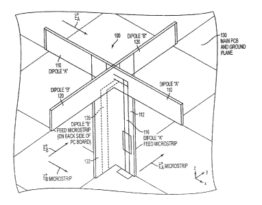
[0003] Orthogonal dipoles are used in many known antennas to provide
dual polarization. For example, FIG. 1 is a schematic view of an apparatus
100 with orthogonal dipoles and associated feed systems as known in the art.
As seen in FIG. 1, the apparatus 100 can include first and second interlacing
members 112, 122. Notches or other cut-outs can be included in each
member 112, 122 to facilitate the members 112, 122 sliding together to
interlace.
[0004] Each member 112, 122 can include a center support structure
and a dipole 110 (Dipole A), 120 (Dipole B), respectively. However, it is to
be
understood that each member 112, 122, including its respective center
support structure and dipole 110, 120, can be one integral member. In some
1
CA 02772517 2012-03-23
embodiments, the members 112, 122 can be mounted to a main printed
circuit board (PCB) 130 that functions as a ground plane.
[0005] A seen in FIG. 1, a first feed microstrip 116 can be disposed on
at least a portion of the center support structure of the first member 112,
and
a second feed microstrip 126 can be disposed on the center support structure
of the second member 122. In some embodiments, the feed microstrips 116,
126 can include tuning elements, such as inductors, capacitors, and
transformers.
[0006] The first feed microstrip 116 can be associated with the first
dipole 110, and the second feed microstrip 126 can be associated with the
second dipole 120. As seen in FIG. 1, the first feed microstrip 116 and the
first dipole 110 can be in the same plane, for example, a plane parallel to
the
X-Z plane. Similarly, the second feed microstrip 126 and the second dipole
120 can be in the same plane, for example, a plane parallel to the Y-Z plane.
[0007] In the apparatus 100 shown in FIG. 1, if the dipoles 110, 120
have coincident centers and are perfectly orthogonal to one another, no
coupling will occur between the dipoles 110, 120 themselves. However, the
apparatus 100 will still provide poor isolation characteristics because
coupling
can occur between each dipole and the orthogonal dipole's feed microstrip.
For example, this coupling can occur because the electric field of one dipole
is
parallel with the electric field of the orthogonal dipole's feed microstrip.
[0008] As seen in FIG. 1, the first feed microstrip 116 associated with
the first dipole 110 is oriented such that its electric field EA MICROSTRIP is
parallel
to the electric field for the second dipole 120, EB. Accordingly, coupling
2
CA 02772517 2012-03-23
occurs between the second dipole 120 and the feed microstrip 116 for the first
dipole 110.
[0009] The feed microstrip 126 associated with the second dipole 120
is oriented such that its electric field EB MICROSTRIP is parallel to the
electric field
for the first dipole 110, EA. Accordingly, coupling occurs between the first
dipole 110 and the feed microstrip 126 for the second dipole 120.
[0010] FIG. 2 is a graphical representation of the isolation achieved by
prior art systems, for example, the apparatus 100 shown in FIG. 1. As seen in
FIG. 2, the isolation can be relatively poor. However, because inter-port
isolation is an important factor in antenna performance, these types of poor
isolation characteristics are undesirable.
[0011] To improve isolation in known antennas, parasitic structures
have been placed near radiating elements. The addition of parasitic
structures has somewhat improved isolation because the mutual coupling
provided by the parasitic elements can help to cancel a portion of the
existing
coupling between the two polarizations. However, the use of parasitic
elements to improve isolation can have adverse effects on the radiation
pattern performance of the antenna. Furthermore, parasitic elements typically
provide only modest improvements in isolation, but increase cost.
[0012] In view of the above, there is a need for a dual polarized
antenna and associated feed system with improved isolation.
BRIEF DESCRIPTION OF THE DRAWINGS
[0013] FIG. 1 is a schematic view of an apparatus with orthogonal
dipoles and associated feed systems as known in the art;
3
CA 02772517 2012-03-23
[0014] FIG. 2 is graphical representation of the isolation achieved by
prior art systems;
[0015] FIG. 3 is a schematic view of an apparatus with dipoles and feed
systems in accordance with disclosed embodiments;
[0016] FIG. 4 is a graphical representation of the isolation achieved by
the apparatus shown in FIG. 3; and
[0017] FIG. 5 is a schematic view of first and second baluns in
accordance with disclosed embodiments.
DETAILED DESCRIPTION
[0018] While this invention is susceptible of an embodiment in many
different forms, there are shown in the drawings and will be described herein
in detail specific embodiments thereof with the understanding that the present
disclosure is to be considered as an exemplification of the principles of the
invention. It is not intended to limit the invention to the specific
illustrated
embodiments.
[0019] Embodiments disclosed herein include a dual polarized antenna
and associated feed system with high isolation. For example, an apparatus in
accordance with disclosed embodiments can achieve high isolation by
orienting the electric field of each dipole parallel to only the electric
field of that
dipole's feed microstrip. That is, the electric field of each dipole can be
orthogonal to an electric field of the other dipole's feed microstrip as well
as to
the electric field of the other dipole itself.
[0020] FIG. 3 is a schematic view of an apparatus 300 with dipoles and
feed systems in accordance with disclosed embodiments. As seen in FIG. 3,
4
CA 02772517 2012-03-23
the apparatus 300 can include a center support structure 310, a first dipole
320 (Dipole A), and second dipole 330 (Dipole B).
[0021] For example, the center support structure 310 can include feed
microstrips 312-1, 312-2, 312-3, 312-4 connecting the dipoles 320, 330 to a
feed system on or below a main PCB 340 that functions as a ground plane. It
is to be understood that the apparatus 300 could include any number of feed
microstrips as would be known by those of skill in the art and is not limited
to
the four feed microstrips shown in FIG. 3.
[0022] It is also to be understood that the feed microstrips are not
limited to the shape of a strip as shown in FIG. 3. Instead, the feed
microstrips could be a transmission line having any shape as would be known
by those of skill in the art. For clarity, the transmission lines between feed
systems and dipoles will be referred to as feed microstrips herein.
[0023] Feed microstrips 312-1, 312-3 can electrically connect the first
dipole 320 to the feed system above or below the ground plane 340, and feed
microstrips 312-2, 312-4 can electrically connect the second dipole 330 to the
feed system above or below the ground plane 340. As seen in FIG. 3, the
feed microstrips 312-1, 312-3 can be in a plane that is parallel to the Y-Z
plane, and the feed microstrips 312-2, 312-4 can be in a plane that is
parallel
to the X-Z plane.
[0024] In some embodiments, the microstrips 312-1, 312-3, 312-3, 312-
4 can be disposed on and/or be supported on or by one or more PCB's, for
example, PCB's 310-1, 310-2, 310-3, 310-4. However, it is to be understood
that the apparatus 300 could include any number of supporting PCB's as
would be known by those of skill in the art and is not limited to the four
PCB's
CA 02772517 2012-03-23
shown in FIG. 3. For example, the apparatus 300 could include any number
of PCB's that is divisible by four.
[0025] When the microstrips 312-1, 312-2, 312-3, 312-4 are disposed
on more than one PCB, as shown in FIG. 3, conductive surfaces of the PCB's
310-1, 310-2, 310-3, 310-4 can be connected at the corners thereof. For
example, solder can be applied to each corner to facilitate the electrical
continuity and conductivity between the PCB's 310-1, 310-3, 310-3, 310-4.
[0026] The first dipole 320 can include a first conductor 323 electrically
connected to the feed microstrip 312-1 and a second conductor 325
electrically connected to the feed microstrip 312-3. In some embodiments,
the conductor 323 can be supported on or by a dielectric support structure
322, and the conductor 325 can be supported on or by a dielectric support
structure 324.
[0027] Similarly, the second dipole 330 can include a first conductor
333 electrically connected to the feed microstrip 312-2 and a second
conductor 335 electrically connected to the feed microstrip 312-4. In some
embodiments, the conductor 333 can be supported on or by a dielectric
support structure 332, and the conductor 335 can be supported on or by a
dielectric support structure 334.
10028] When the feed microstrips 312-1, 312-2, 312-3, 312-4 are
disposed on PCB's, each of the PCB's 310-1, 310-2, 310-3, 310-4 can include
a key, notch, or other type of cut-out known by those of skill in the art to
receive or otherwise mechanically engage a proximate end of the respective
conductors 323, 333, 325, 335 and/or respective dielectric support structures
322, 332, 324, 334. In some embodiments, solder can be applied to the
6
CA 02772517 2012-03-23
mechanical connection of the feed microstrips 312-1, 312-3, 312-3, 312-4 and
the respective conductive strips 323, 333, 325, 335 to facilitate the
electrical
conductivity there between.
[0029] The arrangement of the dipoles 320, 330 and feed microstrips
312-1, 312-2, 312-3, 312-4 relative to one another can enable the apparatus
300 to achieve high isolation. For example, the electric field of each dipole
can be parallel with only the electric field of its own feed microstrips.
Thus,
the electric field of each dipole can be orthogonal to an electric field of
the
other dipole's feed microstrips as well as to the electric field of the other
dipole
itself.
[0030] Specifically, the electric field EA of the first dipole 320 can be
parallel with only the electric field EA MICROSTRIP of the feed microstrips
312-1,
312-3 for the first dipole 320. Similarly, the electric field EB of the second
dipole 330 can be parallel with only the electric field EB MICROSTRIP of the
feed
microstrips 312-2, 312-3 for the second dipole 330. Accordingly, the electric
field EA of the first dipole 320 and the electric field EA MICROSTRIP of the
feed
microstrips 312-1, 312-3, for the first dipole 320 can be orthogonal to the
electric field EB of the second dipole 330 and the electric field EB
MICROSTRIP of
the feed microstrips 312-2, 312-3 for the second dipole 330.
[0031] As seen in FIG. 3, the first conductor 323 of the first dipole 320
can extend away from the first microstrip 312-1 of the center support
structure
310, and the second conductor 325 of the first dipole 320 can extend away
from the third microstrip 312-3 of the center support structure 310. That is,
a
center line of the conductors 323, 325 of the first dipole 320 can be in a
plane
7
CA 02772517 2012-03-23
that is parallel to the X-Z plane of the apparatus 300 so that the
polarization of
the first dipole 320 is parallel with the X axis.
[0032] In accordance with disclosed embodiments, the conductors 323,
325 of the first dipole 320 can be any shape and can be rotated in any
direction as long as a center line of the conductors 323, 325 of the dipole
320
stays a plane that is parallel to the X-Z plane. As explained above and as
seen in FIG. 3, the feed microstrips 312-1, 312-3 for the dipole 320 can be in
a plane parallel to the Y-Z plane. When a center line of the conductors 323,
325 of the dipole 320 is in a plane parallel to the X-Z plane, but the feed
microstrips 312-1, 312-2 for the dipole 320 are in a plane parallel to the Y-
Z,
the electric field EA of the first dipole 320 can maintain the parallel
relationship
with the electric field EA MICROSTRIP of the feed microstrips 312-1, 312-3 as
described above.
[0033] The first conductor 333 of the second dipole 330 can extend
away from the second microstrip 312-2 of the center support structure 310,
and the second conductor 335 of the second dipole 330 can extend away
from the fourth microstrip 312-4 of the center column. That is, the conductors
333, 335 of the second dipole 330 can be in a plane parallel to the Y-Z plane
of the apparatus 300 so that the polarization of the second dipole 330 is
parallel with the Y axis.
[0034] In accordance with disclosed embodiments, the conductors 333,
335 of the second dipole 330 can be any shape and can be rotated in any
direction as long as a center line of the conductors 333, 335 of the dipole
330
stays in a plane parallel to the Y-Z plane. As explained above and as seen in
FIG. 3, the feed microstrips 312-2, 312-4 for the dipole 330 can be in a plane
8
CA 02772517 2012-03-23
parallel to the X-Z plane. When a center line of the conductors 333, 335 of
the dipole 330 is in a plane parallel to the Y-Z plane, but the feed
microstrips
312-2, 312-4 for the dipole 330 are in a plane parallel to the X-Z plane, the
electric field EB of the second dipole 330 can maintain the parallel
relationship
with the electric field EB MICROSTRIP of the feed microstrips 312-3, 312-4 for
the
second dipole as described above.
[0035] As explained above, the apparatus 300 shown in FIG. 3 can
achieve high isolation between dipoles and feed systems. For example,
coupling between a dipole and an orthogonal dipole's feed microstrip can be
greatly reduced and, in some embodiments, substantially eliminated.
[0036] FIG. 4 is a graphical representation of the isolation achieved by
the apparatus 300 shown in FIG. 3. As seen in FIG. 4, the isolation between
dipoles and feed systems can be substantially improved as compared to
known art, for example, the apparatus 100 shown in FIG. 1.
[0037] In some embodiments disclosed herein, the apparatus 300
shown in FIG. 3 can include symmetrical and balanced feed systems for each
dipole 320, 330. For example, first and second baluns 510, 520 can be
employed.
[0038] FIG. 5 is a schematic view of first and second baluns 510, 520 in
accordance with disclosed embodiments. The first balun 510 can be
associated with the first dipole 320, and the second balun 520 can be
associated with the second dipole 330. Two baluns can be employed
because, according to disclosed embodiments, a balun is required for each
polarization to make the unbalanced to balanced transformation from input
microstrips 530.
9
CA 02772517 2012-03-23
[0039] In embodiments disclosed herein, geometric limitations prevent
the baluns 510, 520 from being disposed in the same plane without crossing
one another. Therefore, the first balun 510 can be disposed in a first plane,
and the second balun 520 can be disposed in a second plane provided that
the first and second planes are different.
[0040] For example, as seen in FIG. 5, the first balun 510 can be
disposed on a plane parallel to the ground plane 340, and the second balun
520 can be disposed on a plane parallel with an auxiliary PCB 525. In some
embodiments, the auxiliary PCB 525 can be orthogonal to the ground plane
340. In other embodiments, the first balun 510 can be disposed on a plane on
a first side of the ground plane 340, and the second balun 520 can be formed
on a plane on a second side of the ground plane 340. However,
embodiments disclosed herein are not limited to the placement or orientation
of the planes as long as the plane of the first balun 510 is different than
the
plane of the second balun 520.
[0041] In some embodiments, one or both of the baluns 510, 520 can
be of approximately one half wavelength or any odd multiple thereof.
However, embodiments disclosed herein are not so limited.
[0042] From the foregoing, it will be observed that numerous variations
and modifications may be effected without departing from the spirit and scope
of the invention. It is to be understood that no limitation with respect to
the
specific system or method illustrated herein is intended or should be
inferred.
It is, of course, intended to cover by the appended claims all such
modifications as fall within the spirit and scope of the claims.