Note: Descriptions are shown in the official language in which they were submitted.
CA 2773073 2017-03-28
MONITORING DEVICES AND PROCESSES BASED ON TRANSFORMATION,
DESTRUCTION AND CONVERSION OF NANOSTRUCTURES
10 FIELD OF INVENTION
This invention relates to devices and associated processes based on physical,
chemical
and biological destruction of nanostructures. This invention also relates to
monitoring the
total exposure to organic, inorganic, organometallic and biological compounds
and agents
using unstable, reactive or destructible nanostructures using analytical
methods.
BACKGROUND OF THE INVENTION
US patent application Ser No 12/478,232 discloses certain formulations and
devices
based on the etching of a thin (e.g., 10-100 nm) layer of a metal and fine (1-
50 microns)
particles (destruction of a nano-structure) including some methods for
monitoring and
measuring concentrations of chemical and biological agents.
A nanostructure is an object made from an atom or molecule to a microscopic
size.
Except a quantum dot, nanostructures have at least one dimension usually
between 1 and 100
nanometers and usually a narrow size distribution. A lightly metallized
plastic film, has one
dimension on the nanoscale, i.e., only the thickness of the metal layer is
between 0.1 and 100
nm. Nanowires are one dimensional, nanotubes have two dimensions on the
nanoscale, i.e.,
the diameter of the tube is between 0.1 and 100 nm; its length could be much
greater. Finally,
spherical nanoparticles have three dimensions on the nanoscale, i.e., the
particle is between
0.1 and 100 nm in each spatial dimension.
Materials reduced to the nanoscale can show very different properties compared
to
what they exhibit on a macro scale, enabling unique applications. For
instance, opaque
substances become transparent (copper), inert materials attain catalytic
properties (platinum),
stable materials turn combustible (aluminum), solids turn into liquids at room
temperature
(gold) and insulators become conductors (silicon). Materials, such as gold,
which is
chemically inert at normal scales, can serve as a potent chemical catalyst at
nanoscales. Much
1
CA 02773073 2012-03-02
WO 2011/031959
PCT/US2010/048417
of the interest in nanotechnology stems from the unique quantum and surface
phenomena that
a matter exhibits at the nanoscale.
Nanostructures often have unusual visual properties because they are small
enough to
confine their electrons and produce quantum effects. For example gold
nanoparticles appear
deep red to black in solution. As there is a gradual transition from normal
nano (e.g., 10 nm)
to a nanometer and lower, there will be several other changes in properties at
an atomic level
and hence can undergo a variety of changes.
Nanotechnology is used in many commercial products and processes.
Nanomaterials
are used to add strength to composite materials used to make lightweight
tennis rackets,
baseball bats, and bicycles. Nanostructured catalysts are used to make
chemical
manufacturing processes more efficient, saving energy and reducing the waste
products. A
few pharmaceutical products have been reformulated with nanosized particles to
improve
their absorption and make them easier to administer. Opticians apply
nanocoatings to
eyeglasses to make them easier to keep clean and harder to scratch.
Nanomaterials are
applied as coatings on fabrics to make clothing stain resistant and easy to
care for.
Nanoceramics are used in some dental implants, or to fill holes in bones after
removing a
bone tumor, because their mechanical and chemical properties can be tuned to
match those of
the surrounding tissue. Many electronic devices manufactured in the last
decade use some
nanomaterials. Nanotechnology is used much more extensively to build new
transistor
structures and interconnects for the fastest, most advanced computing chips.
Characterization of nanostructures is done by using a variety of different
techniques, such as
electron microscopy, atomic force microscopy (AFM), dynamic light scattering,
X-ray
photoelectron spectroscopy, powder X-ray diffractometry, fourier transform IR,
matrix-
assisted laser desorption, time-of-flight mass spectroscopy and UV visible
spectroscopy.
A number of devices and products are reported based on nanostructures. Those
devices and products are based on stable nanostructures.
Nanostructures are intrinsically less stable than their counter
microstructures.
There are many reports on making nanostructures, their unique properties and
products made from them, for example, A. Henglein., Chem, Rev., 89 (1989)
1861; M. B.
Mohamed, C. Burda, and M. A. El-Sayed, Nanolett., 1 (2001) 589; J. H. Fendler,
Chem.
Mater., 8 (1996) 1616; C. R. Henry, Surf. ,S'ci. Rep. 31, 231 (1998). There
are no reports,
however, on devices and processes based on destruction of nanostructures.
SUMMARY OF THE INVENTION
2
CA 02773073 2012-03-02
WO 2011/031959
PCT/US2010/048417
Thus it is an object of the invention to use this phenomenon to create a
variety of
devices, products and processes. It is also an object of the present
inventions to develop
devices, products and processes based on (1) destruction, including reduction
in size of
nanostructures, (2) higher reactivity of nanostructures, (3) rapid change in
properties when
size of nanostructures is changed, (4) using unstable nanostructures and
alike.
Thus, this invention relates to an indicating system which comprises a
nanostructure;
and a means to measure the change in properties of the nanostructure as it is
destroyed. In the
indicating system the destruction is due to one or more of: melting, fusion,
dissolution,
swelling, drying, etching, coagulation, conversion, transformation,
crystallization, formation
of defects, decomposition, reaction, diffusion, complex or adduction
formation,
transformation, phase, reactivity, state, size, shape, nature of doping,
magnetism, porosity,
permeability degradation, decay, corrosion, decomposition, disintegration,
deterioration, de-
metallization, coalescence, adsorption, desorption, melting, crystallization,
phase change,
electronic or nuclear structure, magnetism, and optical properties. The
nanostructure is
typically less than about 1,000 nm in at least one dimension.
The nanostructure is comprised of one or more structures selected from the
group of
nanoantenna, nanoballs, nanobelts, nanobipods, nanocapsules, nanocluster,
nanocrystals,
branched nanocrystals, nanodendrimers, nanodots, nanofilms, nanofibers,
nanoflakes/sheets,
nanofluids, nanolayers, nanoparticles, nanorods, nanospheres, nanosprings,
nanotatrapods,
branched tetrapods, nanotripods, nanotubes, nanowires, plasmon, quantum dots,
and quantum
wells. The nanostructure is generally a reactive or unstable organic,
inorganic, organo-
metallic or a biological material and can also be made from a metal, such as
for example,
copper, zinc, magnesium, aluminum, gold, silver silicon, or their alloys.
The indicating system of the invention is based on the destruction of a
nanostructure
wherein the nanostructure is destroyed by an analyte or activator. The analyte
can be selected
from a chemical or biological agent. In one embodiment, the chemical agent is
a toxic or
hazardous chemical. In another embodiment, the biological agent is a virus or
a bacterium.
In yet another embodiment, the analyte is energy, electromagnetic radiation,
pressure,
or magnetism.
The invention also relates to a process of measuring change in a property of a
nanostructure during its destruction, as described more fully below.
Another embodiment relates to a process of changing the performance of an
indicating nanostructure device which comprises changing a non-linear
performance of the
3
CA 02773073 2012-03-02
WO 2011/031959
PCT/US2010/048417
indicating device to a linear performance by increasing the size distribution
of the
nanostructures in the indicating system.
In one embodiment of the invention, the indicating system is designed for use
in
monitoring total exposure to organic, inorganic, organometallic and biological
compounds
and agents or analytes using analytical methods.
In another embodiment of the invention, the indicating system is designed for
monitoring time, time-temperature, thaw, freeze, humidity, ionizing radiation,
temperature,
microwave, sterilization, chemicals, biological or chemical agents, wherein
the sterilization is
done with steam, ethylene oxide, plasma, formaldehyde, dry heat, hydrogen
peroxide or
peracetic acid.
In yet another embodiment, the indicating system of the invention is a
radiation
dosimeter, such as a capacitor.
In the indicating system of the invention the nanostructure can be an
electrode, such
as an organic or inorganic conductor, semiconductor or metal electrode.
In some aspects of the invention, the nanostructure is protected by a coating
or
stabilizing material which is a precursor, activator or transparent conductor.
A preferred
precursor is a halo-compound.
In one aspect of the invention the destruction of the nanostructure is
determined an
analytical method, including an electroanalytical method, such as, for example
ellipsometry.
A main objective of this invention is to provide a system of indicating
devices for
monitoring materials and processes such as time, temperature, time-
temperature, thaw,
freeze, humidity, ionizing radiation, microwave, sterilization (including
steam, ethylene
oxide, plasma, formaldehyde, dry heat, hydrogen peroxide and peracetic acid),
chemicals,
biological and chemical agents, and electronic devices, such as RFID (radio
frequency
identification device) and EAS (Electronic article surveillance), printed
electrodes and alike
based on destruction of nanostructures.
In one aspect of the invention there are provided reactive/destructible
nanosensor
systems for monitoring a variety of processes such as time, temperature, time-
temperature,
thaw, freeze, humidity, ionizing radiation, microwave, sterilization
(including steam, ethylene
oxide, plasma, formaldehyde, dry heat, hydrogen peroxide and peracetic acid),
chemicals,
biological and chemical agents, and electronic devices, such as RFID and EAS,
printed
electrodes and alike based on the destruction of nanostructures.
4
CA 02773073 2012-03-02
WO 2011/031959
PCT/US2010/048417
Also provided are sensors and similar devices made from destructible
nanostructures
that convert physical, biological or chemical input into an electrical or
optical signal. The
signal measures and transforms into digital format which can then be processed
and analyzed
efficiently by computers. The information can be used by either a person or an
intelligent
device monitoring the activity to make decisions that maintain or change a
course of action.
Additionally there is provided a system/device that measures a substantially
irreversible change in physical or chemical properties of nanostructure and
provides a signal
which can be read by an observer or by an instrument.
In aspects of the invention related to analytes, there is are preferred
nanostructures
which are unstable and reactive to analytes or activators.
Also provided is a process of monitoring analytes composed of certain ions and
metals, such as those of toxic elements, such as lead (Pb), mercury (Hg),
arsenic (As),
chromium (Cr), cadmium (Cd), barium (Ba), silver (Ag), and selenium (Se) pose
significant
health risks when present in water supplies with a destroyable nanostructure.
It is an additional object of the invention to provide methods for monitoring
agents
using a sensor having a destroyable nanostructure. The methods include
noncontact and
nondestructive methods, such as optical technique, spectroscopic and
ellipsometry.
Also provided are devices and methods for determination of change in
properties due
of a destruction of a nanostructure with analytic equipment or technique.
Provided also are methods and devices for the creation of nanostructures and
quantum
devices, such as nanoantenna, nanowires, nanodots and quantum dots, e.g., by
the etching or
dissolution of metals and their alloys, semi-metals, semi-conductors and doped
organic and
inorganic materials including semiconducting and conducting materials, such as
conducting
polymers.
Provided are methods for monitoring analytes, such as chemical and biological
agents
using a destructible nanostructure, e.g., a very thin layer or nano sized
particles of electrically
conductive materials, such as metals, alloys and/or an oxide layer on them.
They also include
use of the assembly as an electrode or electrochemical sensors.
Provided are methods of creating a wide range of devices, such as light
emitting
devices, capacitors, batteries, catalysts, electrochemical sensors, biosensors
and materials,
such as structural materials and the like by destruction of nanostructures or
a layer or
component having a nanostructure.
5
CA 02773073 2012-03-02
WO 2011/031959
PCT/US2010/048417
Provided are methods of making non-linear changes in properties of the
indicating
devices based on destruction of nanostructures to linear changes in
properties.
Provided are methods of making non-linear changes in properties of the
indicating
devices based on destruction of nanostructures to linear changes in properties
by using broad
distribution of the nanostructures.
Provided are nanostructures coated with at least one pre-cursor.
Provided are methods of coating nanostructures with a pre-cursor.
Provided are methods of monitoring changes in destructible nano-structures by
visual
and analytical methods.
Provided are indicating devices based on destructible nanostructures which are
smaller than 5 nm.
Also provided are laminates of nanostructures which deteriorate upon exposure
to an
agent or analyte.
The reactive/destructible nanosensors of the invention can be dosimeters for
monitoring radiation, ionizing radiation, X-ray, gamma ray, electrons, protons
and neutrons.
The dosimeters for monitoring ionizing radiation monitor change in electrical
resistance,
capacitance, optical properties and thickness, using, for example, LED,
capacitor, diffraction
grating, diode and photocell containing reactive/destructible nanosensors.
Also provided are methods for monitoring ionizing radiation using
reactive/destructible nanosensors as dosimeters.
In addition there is provided a destructible layer of nanostructures
comprising at least
one nanostructure. wherein the nanostructure layer is optically transparent,
semitransparent,
semiconductive and/or electrically conductive.
Also provided is a machine, apparatus, equipment for determination of effect
of an
activator on a destructible nanostructure including
indicator/electrode/conductor connected to
a power source.
Provided is a machine, apparatus, equipment wherein effect of activator on a
destructible nanostructure including indicator/electrode/conductor is
determined by
determining change in electromagnetic properties.
In another aspect of the invention there is provided a system for
simultaneously
monitoring multiple analytes in a sample using a destroyable quantum dot (QD).
Also provided is an indicating system for simultaneously monitoring multiple
analytes
in a sample, comprising: a first irreversibly reactive QD that reacts to a
first analyte; a second
6
CA 02773073 2012-03-02
WO 2011/031959
PCT/ES2010/048417
reactive QD that reacts to a second analyte; and so on. There may be one or
more quencher,
for quenching the emissions of QDs.
Also provided is an indicating system having more than one destructible
nanostructure including quantum dots that comprise at least one member
selected from the
group consisting of CdS, CdSe, CdTe, ZnS, ZnSe, ZnTe, Pin, PbSe, CdZnSe and a
destroyable nanostructure.
Also provided are methods of destruction, including methods of making
nanostructures from materials which are susceptible to analytes and a
technique for creating
destroyable nanostructures by etching larger nanostructures.
Diode and electronic devices of the invention include an apparatus comprising
a
destroyable Schottky diode made from inorganic and organic semi-conductors
having one or
more destroyable components. Such diode can be comprised of a silicon
substrate; an
ultrathin destroyable metal film located on a portion of said silicon
substrate; said ultrathin
metal film and said silicon substrate together forming a Schottky barrier
having the current-
voltage characteristics of a diode thereby enabling detection of a surface
adsorbate/reaction
on said ultrathin destroyable metal film; wherein the presence of said surface
adsorbate
creates a measurable current resulting from production of electrons or holes
having sufficient
energy to transverse said ultrathin metal film and cross said Schottky
barrier; an oxide layer
formed on said silicon substrate and having an inclination formed therein; and
at least one
zero force electrical contact including a metalized contact electrically
connected to said
ultrathin destroyable metal film; said metalized contact being deposited on
said oxide layer
and wherein said ultrathin metal includes a portion deposited on top of said
inclination in the
oxide layer before being connected to the metalized contact.
Also provided is destroyable capacitor having two reactive metal layers having
thickness in nanometers and a dielectric layer which has capability of
producing an activator
when subjected to an analyte, such as electromagnetic radiation (e.g., X-ray)
and magnetism.
Still another object is to provide a partially demetallized semiconductive
metal
susceptor for microwave indicator wherein the heat produced in different areas
can be
precisely controlled and the various areas producing different amounts of heat
can be given
any desired shape.
BRIEF DESCRIPTION OF THE FIGURES
Figure 1 shows a schematic presentation of changes in some properties of nano
materials with the size of nanostructures.
7
CA 02773073 2012-03-02
WO 2011/031959
PCT/US2010/048417
Figure 2 shows a schematic presentation of a change in a property, such as
transparency or electrical resistance with the thickness of metallized
(aluminized) plastic film
or aluminum particles during an etching process.
Figure 3 shows a schematic presentation of a change in (disappearance or
absence of)
a property upon the destruction of a nanostructure.
Figure 4 shows a schematic presentation of the creation of a nanowall (b),
nanorod
(c), thin nanofilm (d), nanowire/fiber (e) and quantumdot/nanodot (f) by
selective etching of
a nanofilm (a) on a substrate (e.g., a metallized plastic film).
Figure 5 shows a schematic presentation of a dosimeter sensor device made from
nanowires (1) and two electrodes with terminals (2) on a substrate (3). 'the
device may have
coating of a precursor (not shown).
Figure 6 shows a schematic presentation of a change in property with the size
of a
nanostructure having a narrow size distribution (top curve) and with a broad
random
distribution (lower line).
Figure 7 shows a schematic cross sectional presentation of a dosimeter sensor
having
a layer for the transport/injection of an electron (2) between cathode (1) and
an electroactive
layer (3), and a layer for transport of holes (4) between the electroactive
layer and anode (5).
Figure 8 shows a schematic cross sectional presentation of different layers of
a
dosimeter sensor device made from different convertible semiconductor layers,
insulator/dielectric layers and conductors.
Figure 9 shows a schematic cross sectional presentation of a de-activatable
magnetic
EAS system.
Figure 10 shows a schematic cross sectional presentation of a pyro or piezo
electric
de-activatable transducer. The conductive layer can be indium tin oxide (ITO).
Figure 11 shows a flow chart of an apparatus having a nano diffraction grating
as a
sensor. The grating sensor can be an optical fiber.
Figure 12 shows a schematic cross sectional presentation of a dosimeter light
emitting
diode (LED) having a convertible phosphor layer before (a) medium (b) and high
(b) dose of
an analyte, such as X-ray.
Figure 13 shows a schematic cross sectional presentation of a dosimeter
photocell
having a susceptible photo absorbing layer before (a) and after (b) exposure
to an analyte,
such as X-ray.
8
CA 02773073 2012-03-02
WO 2011/031959
PCT/US2010/048417
Figure 14 shows a schematic presentation of a dosimeter/detector diode having
at
least one susceptible component.
Figure 15 shows a schematic presentation of some representative examples of
different types of susceptible nano antennas or sensors.
Figure 16 shows a schematic presentation of dosimeter nano antennas/sensors
made
from different susceptible materials or coated with different precursors for
monitoring
different agents.
Figure 17 shows a schematic presentation of susceptible nano antennas/sensors
coated
with different precursors for monitoring different agents.
Figure 18 shows a schematic presentation of a number of destructible nano
antennas/
sensors connected in a series.
Figure 19 shows a schematic presentation of a number of destructible nano
antennas/
sensors connected in a series and coated with different precursors for
monitoring different
agents. Each antenna/sensor can be made individually addressable.
Figure 20 shows a schematic presentation of a dosimeter device for measurement
of
change in parameters, such as resistance of a conductive or semiconductive
nano layer upon
exposure to analytes.
Figure 21 shows a schematic presentation of a radiation dosimeter device
(capacitor)
and apparatus for measurement of change in more than one parameter, such as
resistance of a
susceptible nano thin electrode and capacitance of the device upon exposure to
high energy
radiation, such as X-ray. An example is described in Example 1
Figure 22 shows a schematic presentation of a radiation dosimeter/sensor
(rolled
capacitor) having two alternating layers of a susceptible nano thin electrode
and a dielectric
layer containing a precursor.
Figure 23 shows a schematic presentation of a radiation dosimeter/sensor
(rolled
capacitor) having a dielectric layer containing a precursor between two layers
of a susceptible
nano thin electrode and a stable dielectric layer.
Figure 24 shows a schematic presentation of a radiation dosimeter/sensor
(rolled
capacitor) having a dielectric layer containing a precursor between two layers
of a non-
destroyable thin electrode and a stable dielectric layer.
Figure 25a shows a photograph of an experimental set up for determination of a
change in resistance of a metallized PET film as a susceptible electrode
having a thin coating
of a precursor (a halocarbon) and then exposed to short wavelength UV light
(blue glow).
9
CA 02773073 2012-03-02
WO 2011/031959
PCT/US2010/048417
Figure 25b shows a photograph of the device of Figure 25a after 2.5 hrs of UV
exposure. Electrical resistance changed from 0.56 kilo Ohms (Figure 25a) to
21.6 mega
Ohms.
DETAILED DESCRIPTION OF THE INVENTION
DEFINITIONS
Unless defined otherwise, all technical and scientific terms used herein have
the same
meaning as commonly understood by one of ordinary skill in the art to which
the invention
pertains. The terminology used herein is for the purpose of describing
particular
embodiments only, and is not intended to be limiting.
Nanostructure: A "nanostructure" is a structure having at least one region or
characteristic
dimension with a dimension of less than about 1,000 nm, e.g., less than about
200 nm, less
than about 100 nm, less than about 50 nm, less than about 10 nm or even less
than a
nanometer. Typically, the region or characteristic dimension will be along the
smallest axis of
the structure. Examples of such structures include nanoantenna, nanoballs
(e.g., fullerenes or
buckyballs), nanobelts, nanobipods, nanocapsules, nanocluster, nanocrystals,
branched
nanocrystals, nanodendrimers, nanodots, nanofilms, nanofibers,
nanoflakes/sheets,
nanofluids, nanolayers, nanoparticles, nanorods, nanospheres, nanosprings,
nanotatrapods,
branched tetrapods (e.g., dendrimers), nanotripods, nanotubes, nanowires,
quantum dots,
quantum wells, others listed herein and alike.
Nanostructures can be substantially homogeneous in material properties, or in
certain
embodiments can be heterogeneous (e.g. heterostructures). Nanostructures can
be, e.g.,
substantially crystalline, substantially monocrystalline, polycrystalline,
amorphous, or a
combination thereof. The material of the nanostructures can be an organic, an
organometallic,
biological or inorganic (metallic, semiconducting and dielectric) chemical.
Nanostructures
can be natural or synthetic bionanostructures. Nanostructures can be
functionalized or
nonfunctionalized. They can be dispersed or coagulated. Nanostructures can be
porous,
hollow, solid, single or multilayered. Nanostructures herein include colloids,
nanoemulsions,
microemulsions and nano-sized liquid crystals, especially when an indicator,
activator,
precursor, additive or coating material is a liquid or semisolid.
Agents and analytes: An agent or analyte is one which has a capability of
reacting or
interacting with a nanostructure or a precursor for an activator and changes
its property. An
agent or analyte include non-materials/energy, such as electromagnetic
radiation, pressure,
magnetism, and materials, such as chemicals including organic, inorganic,
organometallic
CA 02773073 2012-03-02
WO 2011/031959
PCT/US2010/048417
and biological compounds. The term "analyte", "biological analyte" or
"chemical analyte"
means a substance being measured in an analytical procedure. Non-material or
energy type
analytes, such as ionizing radiation, pressure, magnetism and alike which have
substantial
capability of passing through nanostructures and components of the devices
made from a
.. nanostructure and the other types include chemicals, biological agents
which react/interact
usually on the surface of a nanostructure. Time can also be an analyte, for
example, in the
case of time, time-temperature and other devices and processes.
The terms indicator, dosimeter, activator, precursor, binder, metallic,
permeable and
others used herein are as defined or described in Ser No 12/478,232.
.. Destroyable: The destroyable, susceptible and alike nanostructure means a
nanostructure
which undergoes one or more of a sufficiently, usually irreversible,
noticeable or measurable
change in physical, biological or chemical properties, including melting,
fusion, dissolution,
swelling, drying, etching, coagulation, conversion, transformation,
crystallization, formation
of defects, decomposition, reaction, diffusion, complex or adduction
formation,
.. transformation, phase, reactivity, state, size, shape, nature of doping
(e.g., "p" and "n" type),
magnetism, porosity, or permeability and alike.
A nano layer which substantially irreversibly degrades, decays, perishes,
corrodes,
rots, putrefies, decomposes, crumbles, disintegrates, deteriorates, destructs,
becomes unstable
or de-metallizes, undergoes some change in physical or chemical properties is
also included
in the definition of destructible nanostructure.
The destruction of a nanostructure can be due to many processes and materials
including indicator, activator, additives and precursor. The destruction can
be due to many
physical, chemical and biological processes and materials. A chemical
reaction, such as
etching is just one of them. The destruction does not have to complete
destruction of the
.. nanostructure. It can be physical as well. Coalescence, adsorption,
desorption, melting,
crystallization, phase change, electronic or nuclear structure, magnetism,
optical and alike.
Analytical instruments and methods: One or more methods/techniques commonly
used in
the analytical science, including those listed herein.
Sensor/dosimeter/indicator/indicating devices: A sensor means a device made
from a
nanostructure that responds to a stimulus, such as radiation, chemical or
biological stimuli.
The nanostructure can be destroyable. The term sensor, device, dosimeter,
indicator,
indicating devices etc are used interchangeably herein. Indicating devices of
the present
inventions, include devices for measuring for time, time-temperature, thaw,
freeze, humidity,
11
CA 02773073 2012-03-02
WO 2011/031959
PCT/US2010/048417
ionizing radiation, temperature, microwave, sterilization (including that with
steam, ethylene
oxide, plasma, formaldehyde, dry heat, hydrogen peroxide and peracetic acid),
chemicals,
biological and chemical agents, microwave and all other devices (e.g., printed
circuit board,
RFID and EAS), including those defined above and herein. An indicating device
or indicating
.. system also includes other formulations, devices and processes disclosed
herein. We have
also used the word integrator, integrating device, sensor, detector and
monitor and monitoring
devices interchangeably with indicating device and indicating system.
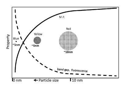
The invention can be described by reference to the Figures. A schematic
presentation
of changes in some properties of nano materials with the size of
nanostructures is shown in
Figure 1. As the size of the nanostructures decreases there usually is a rapid
and non-linear
change in many properties such as the melting point, band gap, color,
fluorescence,
transparency and conductivity. A rapid change in these properties usually
occurs below about
5 nm. Many metals such as gold, copper and silver undergo a rapid change in
color and
fluorescence as the size of the nano particle decreases.
A schematic presentation of change in a property, such as transparency or
electrical
resistance with the thickness of a metallized (aluminized) plastic film or
aluminum particles
during an etching process is shown in Figure 2. When the metal layer is
destroyed, the
product(s) formed is usually transparent with several orders of magnitude
change in electrical
resistance as shown in Figure 25a and 25b. As a nanostructure is destroyed,
simultaneously
there may or may not be the formation of another nanostructure (nanoproduct).
A schematic presentation of change in (disappearance or absence of) a property
upon
destruction of a nanostructure is shown in Figure 3. When the smallest
nanostructure is
destroyed, the resultant product(s) can have a completely different set of
properties (shown
by arrow and question marks "?" in the Figure) from that of the nanostructure.
As the particle
size changes there is often a change in color and/or fluorescence with the
change in the size
of nanospheres. The nanostructure can have any shape, e.g., tube, fiber, rod
etc.
In a reversed process, as small nanoparticles melt, fuse or
coagulate/coalesce, there
will be a change in properties, e.g., color/fluorescence.
A schematic presentation of the creation of nanowalls (b), nanorods (c), thin
nanofilms (d), nanowires/fibers (e) and quantumdots/nanodots (f) by selective
etching of a
nanotilm (a) on a substrate is shown in Figure 4. These nanostructures can
also have a
coating of or be embedded in a protective/stabilizing material (including an
activator,
precursor or a transparent conductor). The activator can destroy these
nanostructures. Some
12
CA 02773073 2012-03-02
WO 2011/031959
PCT/US2010/048417
of these nanostructures can be created by selective etching. If the metal is
an alloy, one can
selectively etch one metal and create nanostructures of the other metal. These
structures, for
example, can be made by first coating the surface with a photo resist, imaging
the resist and
etching the metal. The nanostructures can be coated or embedded with many
activators or
their precursor.
The final nanostructure could be an atom or a molecule. Most likely it will be
small
number of atoms or molecules. If a nanostructure is reacted with a reactant,
e.g., an etchant, it
will reach a stage where the nanostructure will lose its nanodot or quantum
dot properties.
When such thermodynamically stable smallest nano (subnano) structure
disappears, the
properties of a nanodot completely disappear. If the product simultaneously
forms another
nanostructure, a new set of properties of the new nano will appear. Thus,
disappearance of
nanostructure will be associated an extreme change in one or more properties.
This will be a
unique case where there will be a rapid and dramatic change in the properties
of a
nanostructure as its size is reduced and then there will be a sudden
disappearance of that
property.
If a proper precursor is selected it will protect nanostructures from ambient
conditions
and react only to selected analyte.
Metallized plastic film of the desired thickness can be coated with an etch
mask and
etch the undesired portions. The substrate is usually a polymer/dielectric
which could also be
an un-etchable conductive material, such as gold.
Multiple nanostructures can be obtained by coating a etch mask with proper
patterns
followed by etching.
The nanostructure can coated with a dilute solution or by vacuum deposition of
precursor to only cover the nanostructures. All nanostructures can have the
same precursor
coating.
The nanostructure can be completely covered with a precursor or coated with
different
precursors by a nanolithography technique. The nanostructures could be
separate or joined.
The nanowires can be completely covered with a precursor or coated with
different
precursors by a nanolithography technique.
A schematic presentation of a dosimeter sensor device 50 made from nanowires
51
and two electrodes 52, with terminals 54, on a substrate 53 is shown in Figure
5. The device
may have coating of a precursor (not shown). The nanostructure can be any
other than
nanowires.
13
CA 02773073 2012-03-02
WO 2011/031959
PCT/US2010/048417
The terminals can be connected to an analytical instrument. The device can
also be
read with noncontact methods and instruments as well.
A schematic presentation of a change in property with the size of a
nanostructure
having a narrow size distribution (top curve) and with a broad random
distribution (lower
line) is shown in Figure 6. By having a proper distribution of nanoparticles,
a linear change in
properties replaces an otherwise rapid change in properties. One can also use
a broad and
narrow distribution of the nanostructures. A variety of devices can be made by
coating the
broad or narrow distribution of nanostructures on a substrate. If required a
binder, activator
and precursor can be used.
When destructible nanostructures have random distribution, they can provide a
linear
change in a property when etched/destroyed. A linear change in a property is
desirable.
Figure 7 shows a schematic cross sectional presentation of a dosimeter sensor
70
having a layer for transport/injection of electron 72, between cathode 71, and
an electroactive
layer 73, and a layer for transport of holes 74, between the electroactive
layer and anode 75.
The device may have other layers, e.g., precursor or the electroactive layer
may have
a precursor.
Figure 8 shows a schematic cross sectional presentation of different layers of
a
dosimeter sensor devices made from different susceptible semiconductor layers
81, 82 and 83
having different semi-conducting properties, insulator/dielectric layers 85
and conductors 84.
Figure 9 shows a schematic cross sectional presentation of a de-activatable
magnetic
EAS system 90. The device can be composed of a substrate 91 having a layer
susceptible
hard nano magnet 92, a base 93, a susceptible soft nanomagnet 94 and a
protective top layer
95. The properties of susceptible nano-magnets can be adjusted for the device.
The magnets
can have a coating of an activator or precursors (not shown).
Figure 10 shows a schematic cross sectional presentation of a pyro or piezo
electric
de-activatable transducer 100. The device can be made by a susceptible pyro or
piezo electric
nanostructure 103, sandwiched between two conductors which could be conductive
indium
tin oxide (ITO) 102 on a glass or plastic substrate 101.
A flow chart of an apparatus having susceptible nano diffraction grating as a
sensor is
shown in Figure 11. The grating sensor can be an optical fiber having a
coating of a
susceptible nanostructure. Any change in properties of grating can be
monitored using a light
source, coupler, photo detection system and a computer/monitor as an output
system.
14
CA 02773073 2012-03-02
WO 2011/031959
PCT/US2010/048417
Figure 12 shows a schematic cross sectional presentation of a dosimeter light
emitting
diode (LED) 120, having a susceptible phosphor layer 123, before a (a) medium
(b) and high
(b) dose of an analyte, such as X-ray. The phosphor 123 can have a dielectric
layer 122 and
an electrode 121 on one side and a transparent conductor 124 and a transparent
substrate 125
on the other side. The LED will emit light 126 when connected to a proper
power source. As
the phosphor is susceptible to analyte/radiation such as X-ray, upon exposure
to radiation, the
phosphor will be damaged 1231, will be less effective in producing light and
hence will emit
less light, 1261. As the dose increases, the phosphor will become less
effective, 1232 and will
emit less light. The amount of light emitted can be measured by a photo-
detector. Once
calibrated for dose versus light emitted, one can determine the dose.
A schematic cross sectional presentation of a dosimeter photocell 130 having a
susceptible photo absorbing layer before (a) and after (b) exposure to an
analyte/radiation,
such as X-ray is shown in Figure 13. The dosimeter can be composed of a
susceptible
semiconductor 131 in a light absorbing layer 133 can have a transparent
conductor 134 and a
transparent substrate 135 on one side and an electrode for holes 132 on the
other side. When
exposed to a calibrated light source, the dosimeter photocell will generate
current 137 which
can be measured. Upon exposure to an analyte/radiation, the semiconductor
nanostructures
will be damaged 1311 and hence will produce less current 1371. Once calibrated
for dose
versus current produce, one can determine the dose.
Figure 14 shows a schematic presentation of a dosimeter/detector diode 140
having at
least one susceptible component. The diode can be composed of an insulator
141, a gate 142,
channel 143, source 144, drain 145 and a silicone wafer 146. The movement of
electrons 147
will occur between the source 144 and the drain 145. If any destructible layer
of the diode
gets sufficiently damaged by an analyte such as radiation or a toxic agent, it
will not function
as a diode.
The antenna, electrodes or the sensors can have different shapes, sizes,
configurations,
arrangements and thicknesses as required. A schematic presentation of some
representative
examples of different types of susceptible nano antennas or sensors is shown
in Figure 15.
The antenna, electrodes or sensors can be made from different nano materials,
e.g., metals,
semi-metals, semiconductors and non-metals depending upon the devices and
processes. A
schematic presentation of dosimeter nano antennas/sensors made from different
susceptible
materials for monitoring different agents is shown in Figure 16.
CA 02773073 2012-03-02
WO 2011/031959
PCT/US2010/048417
A number of other shapes can also be used. The antenna, electrodes and sensors
for
example, can be in the form of a thin and flat square, triangle including
those mentioned
herein. The antenna can be made from a material destructible by an analyte.
A schematic presentation of susceptible nano antennas/sensors coated with
different
precursors, 171 - 176, for monitoring different agents is shown in Figure 17.
The different
precursors can be used for monitoring different analytes. For example,
halocarbons can be
used for monitoring radiation and humidity sensitive solid activators for
monitoring humidity.
In order to increase the sensitivity of the devices, one can use more than one
antenna/electrode in a series or parallel. A schematic presentation of a
number of destructible
nano antennas/ sensors connected in a series is shown in Figure 18.
A schematic presentation of a number of destructible multisensory nano
antennas/electrodes connected in a series and coated with different precursors
191-198 for
monitoring different agents is shown in Figure 19. Each antenna/sensor can be
made
individually addressable. The antenna can have different shapes. The
antenna/electrodes can
have electronic chips and circuitries as required. For example, RFID have an
electronic chip
and antenna.
Depending upon the nature of the antenna/electrodes one can monitor the change
by
contact or noncontact methods listed herein.
A schematic presentation of a dosimeter device, 20 for the measurement of
change in
parameters, such as resistance of a conductive or semiconductive nano layer,
203 on a
substrate 204 upon exposure to analytes, such as high energy radiation,
humidity and
chemical agents is shown in Figure 20. The device may have a protective or
permeable layer
201. The analyte will interact/react with the precursor layer 202, and produce
an activator.
The activator will etch/destroy or reduce the measurable properties of the
electrode or
antenna 203. By measuring the change in properties of the electrode, one can
measure the
exposure to the analyte.
Figure 21 shows a schematic presentation of a radiation dosimeter device
(capacitor),
21 and apparatus for the measurement of change in more than one parameter,
such as
resistance 215 and capacitance 216 of a susceptible nano thin electrode 212
upon exposure to
high energy radiation, such as X-ray. The device may have a protective layer
211 and a
substrate 214. The precursor layer is sandwiched between the two electrodes. A
demonstration of the concept is shown in Example 1. Upon reaction with
analyte, the
precursor will produce an activator which will react with the electrodes. The
precursor layer
16
CA 02773073 2012-03-02
WO 2011/031959
PCT/US2010/048417
is changing its dielectric properties, the capacitance will change and as the
electrode is etched
away and its resistance will change. Thus, by measuring the capacitance and
resistance, one
can measure the exposure to analytes more accurately.
The capacitor type dosimeters can have a variety of known formats. One of them
is a
rolled capacitor. Because of the higher surface area, a roll capacitor will be
more sensitive for
monitoring lower concentration/exposure to analytes. A few of the designs are
shown in
Figures 22-24.
Figure 22 show a schematic presentation of a radiation dosimeter/sensor in the
form
of a rolled capacitor 22 having two alternating layers of a susceptible nano
thin electrode 221
and a dielectric layer containing a precursor 222.
Figure 23 shows a schematic presentation of a radiation dosimeter/sensor in
the form
of a rolled capacitor, 23 having a dielectric layer containing a precursor 231
between two
layers of susceptible nano thin electrodes 232 and a stable dielectric layer
233.
Figure 24 shows a schematic presentation of a radiation dosimeter/sensor in a
form of
a rolled capacitor, 24 having a dielectric layer containing a precursor 241
between two layers
of non-destroyable thin electrodes 242 and a stable dielectric layer 243.
Figure 25a is a photograph of an experimental setup for the determination of
change
in electrical resistance of a metallized PET (polyester) film as a
susceptible/destroyable
electrode having a thin coating of a precursor (a halocarbon) and then exposed
to short
wavelength UV light. Figure 25b is a photograph of the device of Figure 25a
after 2.5 hrs of
the UV exposure. Electrical resistance changed from 0.56 kilo Ohms (Figure
25a) to 21.6
mega Ohms. The electrode and matching container can be any shaped flat,
square, folded,
zigzag, cylindrical, spiral, etc. The precursor, e.g., halo-compound can be
liquid, emulsion,
viscous liquid, gel, dry coating, paste, etc. Typically, the conductor can be
a metallized
plastic film. The container is preferred to be opaque but can be transparent
with a UV
absorber, i.e., as long as not affected by light. The change in resistance
upon radiation can be
measured by direct contact or non-contact techniques. The preferred
destructible metals are
aluminum, zinc and copper. Once the oxide layer is destroyed by an acid or
base, water can
destroy some of the metals such as aluminum.
Though the change in properties is explained using a specific nanostructure,
such as
rod, dot, sphere, film in the figures above, the nanostructure could be any
other proper
structure suitable for the application.
Analytical methods:
17
CA 02773073 2012-03-02
WO 2011/031959
PCT/US2010/048417
In order to determine a change in a property of a nanostructure and a device
there
from, one can use one or more analytical methods. One or more of the following
analytical
methods can be used for determining change in destructible and non-
destructible
nanos truc lures:
Cyclic voltammetry, electron paramagnetic resonance (EPR) also called electron
spin
resonance (ESR), energy dispersive spectroscopy, ion selective electrode,
e.g., determination
of pH, refractive index, resonance enhanced multiphoton ionization, magnetic
susceptibility,
atomic fluorescence spectroscopy, attenuated total reflectance,
cathodoluminescence,
dielectric spectroscopy, dynamic vapor sorption, differential reflectance
spectroscopy,
electroluminescence, electrophorctic light scattering, electron nuclear double
resonance,
electron paramagnetic resonance spectroscopy, fluorescence correlation
spectroscopy,
fluorescence cross-correlation spectroscopy, glow discharge mass spectrometry,
glow
discharge optical spectroscopy, ion neutralization spectroscopy, low-energy
ion scattering,
nuclear magnetic resonance spectroscopy, optical beam induced current,
optically detected
magnetic resonance, optical emission spectroscopy, photocurrent spectroscopy,
potentiodynamic electrochemical impedance spectroscopy, porosimetry, resonant
inelastic X-
ray scattering, resonance Raman spectroscopy, thermoacoustic tomography, total
internal
reflection fluorescence microscopy, total reflection X-ray fluorescence
analysis, ultrasound
attenuation spectroscopy, ultrasonic testing, X-ray diffuse scattering, X-ray
photoelectron
emission microscopy, X-ray photoelectron spectroscopy, X-ray reflectivity, X-
ray diffraction,
X-ray Raman scattering, X-ray fluorescence analysis, X-ray standing wave and
hybrid or
modified techniques of these methods. The method(s) used depend upon many
parameters,
such as nanostructure, reaction of nanostructure and agent.
Most of the above methods also have several other divisional methods. For
example,
electroanalytical methods includes adsorptive stripping voltammetry,
amperometric titration,
anodic stripping voltammetry, bulk electrolysis, cathodic stripping
voltammetry,
chronoamperometry, coulometry, cyclic voltammetry, differential pulse
voltammetry,
Electrogravimetry, linear sweep voltammetry, normal pulse voltammetry,
Polarography,
potentiometry, rotated electrode voltammetry and staircase voltammetry.
Similarly, most of the above methods and instruments have parts. For example,
electroanalytical analysis instruments can have auxiliary electrode, dropping
mercury
electrode, electrolytic cell, galvanic cell, hanging mercury drop electrode,
ion selective
electrode, mercury coulometer, potentiostat, reference electrode, rotating
disk electrode,
18
CA 02773073 2012-03-02
WO 2011/031959
PCT/US2010/048417
rotating ring-disk electrode, salt bridge, saturated calomel electrode, silver
chloride electrode,
standard hydrogen electrode, ultramicroelectrode and working electrode.
Similarly there are many theories for each method listed above.
It is the beyond the scope of this application to even list all analytical
instruments, methods,
their parts and theories that can be used for the inventions disclosed herein.
Though destructive and direct contact methods can be used, preferred methods
and
instruments are those which determine change in properties without destroying
the sensor and
non-contact.
It is an object of the invention to use or modify these methods or their
hybrids, create
their hybrid for monitoring an agent using a destructible and non-destructible
nanostructure.
For example, once an agent reacts with a thin conductive or metal layer or
precursor for
activator, it can produce compounds which can be monitored with one or more of
these
methods. The metal or oxide on it can act as a catalyst to produce chemicals
which can be
monitored by one or more of these methods. These methods are described in
detail in a
number of books and reviews.
The above and other analytical techniques and instruments can be used for
monitoring change
in properties of nanostructures for the applications/dosimeters disclosed
herein.
Electroanalytical methods:
Electroanalytical methods which measure the potential (volts) and/or current
(amps)
in an electrochemical cell containing an analyte can be used for the present
inventions. These
methods that can be used can be categorized according to which aspects of the
cell are
controlled and which are measured. The three main categories are potentiometry
(the
difference in electrode potentials is measured), coulometry (the cell's
current is measured
over time), and voltammetry (the cell's current is measured while actively
altering the cell's
potential). It is an object of this invention to use these methods, their
modifications,
variations and also their hybrids using a nanostructure, especially
destroyable nanostructure
e.g., a thin layer of a reactive metal and a protective or detector/precursor
layer on the metal
which undergo at least one change in measurable property.
Electrode: A substrate having a nanolayer of a conductive nanomaterial can be
used as an
electrode or electrochemical sensor for one or more of electroanalytical and
non-
electroanalytical techniques described herein. The electrode can be
substantially destructible.
The conductive layer is also referred herein as a metal, organic metal and/or
semiconductive
layer. The conductive nano film can be converted to other nanostructures by
selective etching
19
CA 02773073 2012-03-02
WO 2011/031959
PCT/US2010/048417
and other methods. The substrate for the electrode could be opaque,
translucent or
transparent. The electrode, the metal layer and the substrate could be of any
shape, e.g., a
very thin film/coating, fiber, rod, flat, patterned, hollow, folded, spiral,
zigzag, wounded or
rolled, cylindrical, any irregular shape and addressable. They can be zero
(e.g. nanodots), one
(e.g., thin fiber), two (e.g., thin film) or three dimensional. The substrate
could be an
insulator, semi-conductor, semi-metal, metal or their alloy. The preferred
substrate is plastic
or glass. The substrate could be porous. The electrode could be mono, bi or
multi-layered.
The thickness of the metal or the conductive layer can be from a few Angstroms
to a micron,
preferably 10 ¨ 1,000 Angstroms. A metallized plastic film can be used as an
electrode. The
metal layer can be porous, continuous or particulate. The electrode could be
in form of a
hologram or grating.
Carbon, activated, charcoal, film, fiber, etc can be used as an electrode.
Transparent
conductors, such as indium tin oxide can also be used as an electrode. The
electrode can be
porous or micro-textured.
Aluminum, copper and their alloys can be coated on highly resistive metal or
alloy for
an electrode. This allows one to measure properties even when the
nanostructure is destroyed.
Electrochemical means of quantifying or detecting an analyte is one of the
preferred methods
because of their simplicity, both in terms of device manufacture and in terms
of the ease of
use. Electrochemical sensors have often been in the form of either
potentiometric or
amperometric devices. Potentiometric devices measure the effects of the
charges on atoms
and their positions; examples include the chemFET (chemical field effect
transistor) and the
ion-selective electrode (including pH electrodes). Amperometric devices
operate on the
principle of applying a potential and measuring the resulting current, where
the magnitude of
the current generated is usually related to the amount of analyte present;
alternatively, the
total charge passed over a time may be used to represent the amount of analyte
in a region of
the sample. Because the range of compounds that can generate electrochemical
currents is
smaller than those that carry charges, amperometric devices can often offer
greater
selectivity.
The presence of an analyte in the sample is evaluated in an electrochemical
system
using a conduction cell-type apparatus. A potential or current will be
generated between the
two electrodes of the cell sufficient to bring about oxidation or reduction of
the analyte or of
a mediator in an analyte-detection redox system, thereby forming a chemical
potential
gradient of the analyte or mediator between the two electrodes. After the
gradient is
CA 02773073 2012-03-02
WO 2011/031959
PCT/US2010/048417
established, the applied potential or current is discontinued and an analyte-
independent signal
is obtained from the relaxation of the chemical potential gradient. The
analyte-independent
signal can be used to correct the analyte-dependent signal obtained during
application of the
potential or current. This correction allows an improved measurement of
analyte
concentration because it corrects for device-specific and test specific
factors, such as
transport (mobility) of analyte and/or mediator, effective electrode area, and
electrode
spacing (and as a result, sample volume), without need for separate
calibration values.
The cell or electrochemical cell may have a reference electrode.
A substrate having a nano-structure, e.g.,a thin layer of a conductive
material, such as
metal, organic metal or semiconductor having one or more of (1) a naturally or
artificially
applied protective, permeable or absorbent/adsorbent layer, (2) layer of an
activator, its
precursor, catalyst or modulator can also be used as electrode or electrode
assembly. The
protective layer can be a naturally formed or intentionally added oxide layer
or any other
layer, such as phosphate, zincate, chromate, etc. Electrochemical
electrode/detectors can be
used in mobile detectors to detect blister, nerve, blood, and choking agents.
Thermoelectric conductivity. The electrical conductivity of certain materials
can be
strongly modulated following the surface adsorption of various chemicals.
Heated metal
oxide semiconductors and room-temperature conductive polymers are two such
materials that
have been used commercially. The change in sensor conductivity, especially
when the
electrode is a destroyable nanostructure or undergoes a change in
conductivity, can be
measured using a simple electronic circuit, and the quantification of this
resistance change
forms the basis of sensor technology.
Destruction of electrode: When exposed to an agent in a gas or liquid state,
the agent will
first react with the nano thin oxide/protective layer, if any, and then with
the metal or
conducting nanolayer. Thus, this type of reactive electrode will decay as the
reaction
proceeds. These type of electrodes or nanolayers which degrade, decay, perish,
corrode, rot,
putrefy, decompose, crumble, disintegrate, deteriorate, destruct, become
unstable or de-
metallize, undergo some change in physical or chemical properties are referred
herein as
destroyable electrode/sensor/nanostructure.
Destruction of oxide layer: If a metal has an oxide layer, it can be removed,
thinned,
changed, and made permeable to an agent by adding an agent which selectively
reacts with
the oxide layer. The preferred reagents are chelates. The oxide layer can be
opaque,
transparent, permeable, semi-permeable, selectively permeable, reactive or
destroyable.
21
CA 02773073 2012-03-02
WO 2011/031959
PCT/US2010/048417
For indicating devices disclosed in out US patent application Ser No
12/478,232, the
oxide layer can be obtained by vacuum evaporation of metal under controlled
atmosphere of
oxygen, where metal gets oxidized and an oxide layer is deposited on the said
indicating
layer.
By selecting a proper metal or an alloy, one can minimize or eliminate the
formation
of the oxide layer or impermeable oxide layer. For certain transparent
conductive layers, such
as that of indium-tin-oxide and antimony tin oxide, the conductive and the
oxide layers will
be the same.
The metal nanolayer of the electrode may have an oxide layer. The metal and
oxide
layer can be on, one, both or all sides the substrate. The metal layer may
have one or more
additional organic, inorganic or organo-metallic layers, e.g., protective or
selective, e.g.,
semi-permeable layer. The extra layer can be an absorbent, adsorbent, super
absorbent or
super adsorbent material, especially polymeric material.
The nanolayer of the electrode may have a layer of an activator, pre-cursor,
catalyst,
promotor, additive, retarder, reactant or co-reactant. Some of the activators,
precursors,
catalysts, promotors, reactants and co-reactants are listed, define or
described in our US
Patent Application Ser No 12/478,232 and cited herein as reference. Water or
other
solvents/liquids or ionic liquids can be used as a media, catalysts,
facilitator or modulator.
The media could be solid, liquid, semi-solid, gel, emulsion, gas or plasma.
As used herein, the term "conduction cell" or "conductivity cell" refers to a
device
comprising two electrodes in contact with a medium (e.g., air, gas, solution,
gel, solid), such
that the conductance of the medium can be calculated by passing current
between the
electrodes.
As used herein, the term "effective electrode area refers to the electrode
area that is
in electrolytic/activator/precursor contact with the sample. The effective
electrode area may
be varied by altering the geometry of the electrode or by partial contact of
the electrode to the
sample.
As used herein, the term "electrolytic contact" refers to having an
electrochemical
system comprised of at least one electrode deployed in a manner so as to
gather
electrochemical information from a sample. Examples include, but are not
limited to, an
electrode in physical contact with a sample; an electrode separated from a
sample by a
membrane, a film, or other material; and an electrode separated from a sample
by an aqueous
22
CA 02773073 2012-03-02
WO 2011/031959
PCT/US2010/048417
medium. Examples of electrochemical information include Faradaic current,
nonfaradaic
current and chemical potential.
Surface treatment and pre-treatment of electrode: If required, the electrode
surface can be
pretreated to destroy the naturally oxide or similar protective layers, effect
or phenomenon.
For example, expose the electrode to initial dose of radiation till the oxide
layer is destroyed
by a precursor. One can protect the surface of the electrode with a layer
which is gets readily
destroyed when the electrode is dipped or exposed to a media, environment or
agent. This can
also be done by selecting a metal or an alloy or amalgam which either does not
form an oxide
layer or forms a very thin layer, monolayer which is permeable to precursor.
The surface can
be protected by a very vulnerable layer, such as monolayer which gets
destroyed when the
system is activated. Alternatively, one can pre-treat the surface with an
agent for example,
chlorine or similar agents so that the protective oxide layer is easily
destroyed and/or
converted to permeable layer.
Devices having electrode: 'The devices which require at least one electrode,
especially high
.. electrical conductivity and optical transparency include, but are not
limited to, touch screens
(e.g., analog, resistive, 4-wire resistive, 5-wire resistive, surface
capacitive, projected
capacitive, multi-touch, etc.), displays (e.g., flexible, rigid, electro-
phoretic, electro-
luminescent, electrochromatic, liquid crystal (LCD), plasma (PDP), organic
light emitting
diode (OLED), etc.), solar cells (e.g., silicon (amorphous, protocrystalline,
nanocrystalline),
cadmium telluride (CdTe), copper indium gallium selenide (CIGS), copper indium
selenide
(CIS), gallium arsenide (GaAs), light absorbing dyes, quantum dots, organic
semiconductors
(e.g., polymers, small-molecule compounds), solid state lighting, fiber-optic
communications
(e.g., electro-optic and opto-electric modulators) and microfluidics (e.g.,
electrowetting on
dielectric (EWOD). These devices will not function if the electrode is
destroyable or get
destroyed by an agent, such as chemical or radiation. Hence, one can monitor
an agent by
determining non-functionality, limited functionality or abnormal functionality
of these
devices. Many other analytical techniques and equipment can be used including
those listed
herein.
Ion Mobility Spectrometry (IMS): IMS operates by drawing air at atmospheric
pressure
into a reaction region where the constituents of the sample are ionized. The
ionization is
generally a collisional charge exchange or ion-molecule reaction, resulting in
formation of
low-energy, stable, charged molecules (ions). The agent ions travel through a
charged tube
where they collide with a detector plate and a charge (current) is registered.
A plot of the
23
CA 02773073 2012-03-02
WO 2011/031959
PCT/US2010/048417
current generated over time provides a characteristic ion mobility spectrum
with a series of
peaks. The intensity (height) of the peaks in the spectrum, which corresponds
to the amount
of charge, gives an indication of the relative concentration of the agent
present. This
technology is mainly used in mobile detectors to detect nerve, blister, and
blood agents. If the
charged tube and detector plates are thin conductive and are or have
reactive/destroyable
nanolayers, they will react with an agent and get destroyed as the reaction
proceeds and the
spectrum and many other properties will change irreversibly. It is an object
of this invention
to modify the IMS technique by replacing the charged tube and detector plates
with thin
conductive and reactive/destroyable nanolayers.
Photo Ionization Detectors (PIDs): PIDs operate by passing the air sample
between two
charged metal electrodes in a vacuum that are irradiated with ultraviolet
radiation, thus
producing ions and electrons. The negatively charged electrode collects the
positive ions, thus
generating a current that is measured using an electrometer-type electronic
circuit. The
measured current can then be related to the concentration of the molecular
species present. If
the charged electrodes are thin conductive and reactive/destroyable
nanolayers, they will
react with an agent and get destroyed as the reaction proceeds.
Color-Change indicators: This technology is based upon chemical reactions that
occur
when an agent interacts with various chemicals (either in solution) or coated
on a substrate.
The most common indicator (for a positive response) is a color change.
Detection tubes,
papers, or tickets use some form of surface or substrate to which a reagent
solution is applied.
At nanolevel, these indicating materials will be much more sensitive and a
color
change can occur from I JV to IR. Many of these indicators will undergo a
change in
fluorescence along with the color change. Color change can be monitored
visually as well as
with a spectrophotometer.
It is an object of the present invention to prepare nanolayers of chemicals
which react
with chemical and biological agent and undergo an irreversible change in color
or
fluorescence or by other methods listed herein.
Ellipsometry: The name "ellipsometry" stems from the fact that the most
general state of
polarization is elliptic. Upon the analysis of the change of polarization of
light, which is
reflected off a sample, ellipsometry can yield information about layers that
are thinner than
the wavelength of the probing light itself, even down to a single atomic
layer. Ellipsometry
can probe the complex refractive index or dielectric function tensor, which
gives access to
fundamental physical parameters and is related to a variety of sample
properties, including
24
CA 02773073 2012-03-02
WO 2011/031959
PCT/US2010/048417
morphology, crystal quality, chemical composition or electrical resistance. It
is commonly
used to characterize film thickness for single layers or complex multilayer
stacks ranging
from a few angstroms or tenths of a nanometer to several micrometers with an
excellent
accuracy.
When an agent reacts with a nanostructure, its texture, thickness, resistance,
etc will
change. These changes can be detected by ellipsometric measurements in which
the
ellipsometric parameters are determined. It is an object of the invention to
use ellipsometry
technique and equipment to determine change in texture, thickness, resistance
when a
nanostructure, especially when nanofilm reacts with an analyte/agent.
Electronic noses and electronic tongues: 'There are several gas sensors
available on the
markets among which are metal oxide sensors, often referred to as Tagushi
sensors. They are
composed of metal oxide(s) having a porous form, generally doped with a metal.
They are
operated at elevated temperatures of 100 C to 600 C in order to allow
combustion of the
analyte at the metal oxide surface, inducing a change of oxygen concentration
and therefore a
change in conductance. Metal oxide sensors are generally employed as single
devices to
detect toxic or flammable gases.
If the oxide or other nanolayer undergoes an irreversible change in resistance
and
other properties when it reacts with an analyte, it can be used for monitoring
total exposure to
the analyte. When destroyable nanostructures are used as electronic noses and
tongues, they
can be used for monitoring degradation/spoilage of food, where the nanolayer
is in direct
contact with food (including above food but inside the package). The changes
can be
monitored visually if there is a change in color or transparency or with
noncontact or contact
analytical equipment.
Basic instrumentation: The detecting/monitoring systems proposed herein can
also be
composed of some basic subsystems, (1) Source/supplier unit: The source can be
an electrical
current, electromagnetic ionizing or non ionizing radiation (micro/radio
waves, infrared,
electron, gamma ray, neutron), gas and alike. Power source could be an AC or
DC depending
upon the device. (2) Cell: This could contain many components to support the
nanostructure,
(3) Detector/sensor: To monitor a change occurred in the cell/nanostructure,
(4) Analyzer:
Analytical technique or instrument, such as spectrophotometers (X-ray,
visible, IR,
microwave, FTIR, Raman spectroscopy), electrometer, etc, (5) Processor: A
computer with
the proper software to process the data and (6) Display: A monitor or printer
to show the
changes.
CA 02773073 2012-03-02
WO 2011/031959
PCT/US2010/048417
Capacitor: A capacitor, two parallel conductors separated by a dielectric, can
be formed by
rolling a metalized plastic film that includes a plastic film serving as a
dielectric and two
metal layers serving as electrodes. For a long life of a capacitor, the
plastic film serving as a
dielectric is selected from the group consisting of polyethylene terephthalate
resin,
polypropylene resin, polyethylene naphthalate resin, polycarbonate resin and
the like. The
metal serving as an electrode is selected from the group consisting of zinc
(Zn), aluminum
(Al), aluminum alloy and the like.
A capacitor of the present invention can be composed of two very thin reactive
metal
layers having a thickness in nanometers and a dielectric layer which has
capability producing
an activator when subjected to an analyte, such as electromagnetic radiation
and magnetism.
The destroyable capacitor for monitoring ionizing radiation can be composed of
a very thin
layer of radiation sensitive material, such as polyvinyledene chloride (PVDC)
on a nano thin
conductive layer or between nano thin metallized thin plastic films. There are
many
modifications of the capacitor. For example, a thin PVDC film can be
metallized on both its
sides. The destroyable capacitor can be rolled like other capacitors. In this
case, the precursor
film, such as that of PVDC will produce acids, such as HC1 upon radiation. HC1
will change
the dielectric property of PVDC and/or can react with the thin metal layer and
simultaneously
change the resistance of the electrodes. Materials which undergo change in
dielectric
properties upon radiation can be used as a material for the dielectric layer
that includes
materials which undergo degradation, crosslinking, polymerization and
formation radicals.
The capacitor can also be a nanocapcitor as well. The size of the components
of the
capacitor can be in form nano to any large desired. The destructible
capacitors can be
connected in a series or in a parallel or in a combination of them as needed.
Change in properties, such change in conductivity/resistance, voltage,
current,
capacitance, ability to hold charge and/or combination thereof can be used for
monitoring
action of an agent, such as radiation. The radiation dosimeter capacitor can
be
electrical/electrolytic double layer or ion type.
The destroyable capacitors can be used for monitoring anything which can
diffuse or
pass through the capacitor, especially electromagnetic ionizing or non-
ionizing radiation from
radar/radio (103 meter to 10-12 meter) wave to cosmic wave of mega and giga
volt energy.
Radiowave (103 meter), microwave, IR, visible, UV, X-ray, gamma ray (0.1
Angstrom).
Monitoring the radiation will depend upon the pre-cursor or activator used.
26
CA 02773073 2012-03-02
WO 2011/031959
PCT/US2010/048417
Piezo electric: The dosimeters can also be made by selecting piezoelectric
nano materials
which are sensitive to analyte and change the piezoelectric properties.
According to the
invention, the manufacturing process comprises the stacking of at least one
destroyable
piezoelectric element and of at least two metallic electrodes.
Filters for radiation dosimeters: The dosimeter device could be made of more
than one
dosimeter system, one having no filter while the others having filters, such
as lead, cadmium,
copper, boron etc of different thicknesses for selectively filtering of some
radiation of certain
energy.
Neutron: For monitoring neutrons the dielectric layer can contain compounds
having a high
neutron cross section, such as boron and lithium compounds which produce alpha
particles
when interact with a neutron.
Blood RAD/TTI: Certain perishables, such as fresh blood and some food are
radiated. Once
radiated, they have shelf life. These types of perishables need two
indicators, one for
indicating radiation exposure and the other for indicating shelf life. It is
also possible to use
two radiation dosimeters of different sensitivities for these types of
perishables. The higher
sensitivity will show a change upon radiation while the other will show
radiation and shelf
life. The device, having halocompounds as a precursor, can be used as for
monitoring
radiation and/or time-temperature. Radiation will produce an acid which will
then etch the
metal. As there is a delay, this is good for blood and other foods/perishables
which are
radiated and after radiation they have shelf life. The result of such
radiation followed by the
time-temperature indicator is shown in Figures 25(a) and 25(b) both are visual
and measure
the resistance of the nano thick layer of a metal.
High sensitivity dosimeter: The capacitor can be charged before radiation.
When radiated,
the charged electrode will produce a charged species which will degrade the
destroyable
dielectric layer. One can measure the dose either by measuring the charge,
resistance of the
nano dielectric layer and the nano metal layer or the capacitance of the
capacitor.
Dielectric layer: The dielectric layer of the capacitor can be a destroyable
polymer, such as
PVDC containing halocompounds, such as chloroform or trichloroethane.
Autocatalytic: Production of an activator can be accelerated by an
autocatalytic chain
reaction, e.g., dehydrohalogenation of polymers, such as polyvinylchloride and
polyvinylidene chloride and other halo compounds, such as 1,2,3,4,5,6-
hexachlorocyclohexane and perchlorinated hydrocarbons.
27
CA 02773073 2012-03-02
WO 2011/031959
PCT/US2010/048417
Design: The dosimeter can be made in many different ways and can have many
designs. The
sensor could be disposable and electronic. It could be in the form of a badge
or a table top
unit. The holder can be similar to those available commercially, described in
prior art and in
patent application Ser No 12/478,232. The holder can be composed of an area to
receive the
element/sensor. The dosimeter can be inserted in a unit which can read
properties, such as
conductance, capacitance, charge, etc and read the dose from the calibration.
Proper software
and calibration can be developed and used for calculating the dose.
False signals: The dosimeter can be designed for monitoring false positives,
false negatives,
other undesirable effects of ambient conditions and tampering. The system can
also include
the devices and processes for the correction of the undesired effect of
ambient conditions,
such as time, temperature, time-temperature, shelf life, humidity,
UV/sunlight, air pollutant
and other undesirable ambient conditions.
Two sensors: Two sensors can be supplied to the users, one to be stored away
from the
source of users and the other for monitoring the background dose.
Methods of determination and standards: One can use ASTM methods for
determination
of change in properties. For example, change in volume or surface resistivity
can be
determined by ASTM D 991 and ASTM D 257, respectively.
Use of conducting polymers: Conducting/doped polymers, such as
polyphenylenevinylene,
polyacetylene, polythiophene, polypyrrole, and polyaniline and polyphenylene
sulfide can be
used for making the electrodes. Undoped conducting polymers containing
halocompounds
can be as a dielectric layer. Upon radiation, acids such as HC1, HF or iodine
will increase the
conductance of the layer.
Container/holder: The container for the dosimeter or sensor should preferably
be opaque
and impermeable to protect from UV light and other ambient conditions, such as
impermeable to oxygen and water/humidity.
Medium: Dielectric layer/medium does not have to be solid. The medium can be
liquid, gel,
semisolid, gas, vapor or even a plasma state or mixture thereof. The medium
can be an
emulsion of a halo compound or a mixture thereof with water using preferably
non-ionic
surfactants. The medium can have one more additive to control the reaction,
either to
accelerate or retard. Water is a preferred additive, preferably in the form of
a solution or
emulsion. The dielectric layer can be composed of microemulsion and
nanoemulsion
Thickness: The conductive layer can be a metal, an alloy, a conductive polymer
or a mixture
of conductive polymers. The thickness of the conductive layers and dielectric
layer can be
28
CA 02773073 2012-03-02
WO 2011/031959
PCT/US2010/048417
from a nano meter to microns or thicker. However, one of them should be
thinner and
preferably in the nanometers range.
Halocompounds: Examples of the halogenated organic compounds include
halogenated
hydrocarbons, halogenated alcohols, halogenated ketones, halogenated ethers,
halogenated
esters, halogenated amides, halogenated sulfones, halogenated phosphates, and
halogenated
heterocyclic compounds. In the halogen compound, two or more halogen atoms are
preferably bound to one carbon atom. It is more preferred that three or more
halogen atoms
be bound to one carbon atom.
Examples of the halogenated hydrocarbons include carbon tetrabromide,
iodoform,
ethylene bromide, methylene bromide, amyl bromide, isoamyl bromide, amyl
iodide,
isobutylene bromide, butyl iodide, diphenylmethyl bromide, hexachloroethane,
1,2-
dibromoethane, 1,1, 2,2 -tetrabromoethane, 1,2-
dibromo-1,1,2-trichloroethane, 1,2,3 -
tribromoprop ane, 1 -bromo-4 -chlorobutane, 1,2,3 ,4-
te trabromobutane,
tetrachlorocyclopropane, hexachloro-cyclopentane, dibromocyclohexane, and
1,1,1-trichloro-
2,2-bis(4-chlorophenyl)ethane.
Examples of the halogenated alcohols include 2,2,2-trichloroethanol,
tribromoethanol,
1,3-dichloro-2-propanol, 1,1,1-trichloro-2-propanol,
di(iodohexamethylene)
aminoisopropanol, tribromo-t-butyl alcohol, and 2,2,3-trichlorobutane-1,4-
diol.
Examples of the halogenated ketones include 1,1-dichloroacetone, 1,3-
dichloro acetone , hexachloroacetone, hex abromoacetone, 1,1,3 ,3- tetrachloro
ace tone, 1,1,1-
trichloroacetone, 3 ,4-dibromo- 2-bu tanone, 1 ,4-
dichloro-2-butanone, and
dibromocyclohexanone.
Examples of the halogenated ethers include 2-bromoethyl methyl ether, 2-
bromoethyl
ethyl ether, di(2-bromoethyl) ether, and 1,2-dichloroethyl ethyl ether.
Examples of the halogenated esters include bromoethyl acetate, ethyl
trichloroacetate,
trichloroethyl trichloroacetate, homopolymer or copolymer of 2,3-dibromopropyl
acrylate,
trichloroethyl dibromopropionate, and ethyl alpha, beta-dichloroacrylate.
Examples of the halogenated amides include chloro-acetamide, bromoacetamide,
dichloroacetamide, trichloro-acetamide, tribromoacetamide,
trichloroethyltrichloro-
acetamide, 2-bromoisopropionamide, 2,2,2-trichloro-propionamide, N-
chlorosuccinimide,
and N-bromosuccinimide.
Examples of the halogenated sulfones include tri-bromomethyl phenyl sulfone, 4-
nitrophenyl tribromomethyl sulfone, and 4-chlorophenyl tribromomethyl sulfone.
29
CA 02773073 2012-03-02
WO 2011/031959
PCT/US2010/048417
Examples of the halogenated phosphates include tris(2,3-dibromopropyl)
phosphate.
Examples of the halogenated heterocyclic compound include 2,4-
bis(trichloromethyl)-
6-phenyltriazole.
Particularly preferred halogen compounds are tri-bromomethyl phenyl sulfone
and
2,4-bis(trichloromethyl)-6-phenyltriazole.
Agricultural chemicals including, for example,
ethy1-4-I4-(4-
trifluoromethylphenoxy)phenoxy]-2-pentenoate, butyl-
24445 -trifluoromethy1-2-
pyridyloxy)phenoxy] propionate, N-benzy1-2-isopropylpivalamide, N,N-
dialky1-2-
chl oroacetami de, S-ethyl-N,N-diethyl c arb am ate, 4-octanoyl ox y-3 ,5-
dibromobenzoni tri le, 2-
chloro-2',6'-diethyl-N-(n-propoxyethyl)-acetanilide, 2-(2-chlorobenzylthio)-
5 -propyl- 1 ,3 ,4-
oxadiazole, 2-(1 ,2-
dimethylpropylamino)-4-ethylamino-6-methylthio- 1,3 ,5-triazine,
hexachloroacetone, tris- [2- (2,4-dichlorophenoxy)ethyl] -phosphite, and
2-(2-
chlorophenyl)methy1-4,4-dimethy1-3-isooxazolidinone can also be used.
Preferred are the trihaloacetates wherein all the halogen atoms are the same
and
especially the trichloroacetates. Illustrative of the compounds which can be
employed in the
practice of the present invention are methyl trichloroacetate, ethyl
tribromoacetate, isopropyl
trifluoroacetate, tert-butyl triiodo ace tate, n-octyl
dibromochloroacetate, n-decyl
dichlorofluoro acetate, 1-ethyl- 1-n-propylheptyl
chlorodiiodoacetate, n-pentadecyl
trichloroacetate, n-eicosyl trichloroacetate, cyclopentyl trichloroacetate,
cyclohexyl
trichloroacetate, phenyl trichloroacetate, 1-naphthyl trichloroacetate, 2-
naphthyl
trichloroacetate, cyclopentylmethyl trichloroacetate, 7-cyclohexylheptyl
trichloroacetate,
benzyl trichloroacetate, 3,4 -diphenylbutyl trichloroacetate, 2-
methylcyclopentyl
trichloroacetate, 3,4 -di-n-butylcyclopentyl trichloroacetate, 2,3,4-tri-n-
pentylcyclopentyl
trichloroacetate, 4-methylcyclohexyl
trichloroacetate, 2,4,6-triisopropylcyclohexyl
trichloroacetate, 4-n-dodecylcyclohexyl trichloroacetate, 4-phenylcyclohexyl
trichloroacetate,
4-tetradecylphenyl trichloroacetate, 4-methylphenyl trichloroacetate, 2,4,6-
triethylphenyl
trichloroacetate, 3,5-di-n-butylphenyl trichloroacetate, 4-cyclohcxylphenyl
trichloroacetate,
and the like.
Pre-treated: The device can be pre-radiated to dissolve or to make the oxide
layer thinner or
by adding a controlled amount of an activator/additive, such as HCl or other
etchant so it can
be easily destroyed or thinned to a desired layer. In this case, once an oxide
layer is destroyed
water can react and dissolve the metal layer. A preferred activator/additive
is one which gets
adsorbed on the oxide layer (if it is there).
CA 02773073 2012-03-02
WO 2011/031959
PCT/US2010/048417
Protective layer: If required, in order to protect the metal layer from
forming an oxide layer,
it can be coated with a layer which is non permeable to oxygen and moisture or
with another
very thin layer of a metal, such as copper which can be easily destroyed.
Conducting polymers
The conductive layer can also be made from conductive ink or paint containing
fine particles
of a conductive material, such as metal or conductive polymer. The materials
used for
conducting inks include carbon, copper, silver, aluminum, silver-aluminum,
indium tin oxide,
fluorine doped tin oxide, as well as specialty materials, such as the copper
indium gallium
diselenide (CIGS) for the active layer in some PVs (photovoltaics).
Electrical conductivity can be induced in polymers selected from the group of
substituted and unsubstituted polyanilines, polyparaphenylenvinyles,
substituted and
unsubstituted polythiophenes substituted and unsubstituted poly-p-phenylene
sulfides,
substituted polyfuranes, substituted polypyrroles, substituted
polyselenophene,
polyacetylenes formed from soluble precursors, combinations thereof and blends
thereof with
other polymers.
The polymers may contain a doping precursor, selected from the group of onium
salts,
iodonium salts, triflate salts, borate salts, tosylate salts and
sulfonoxylimides. Conductivity
can be selectively induced in the polymers by selectively doping upon
selective exposure to a
source of energy, such as electromagnetic radiation, e.g., an electron beam or
X-ray.
Dopants: Dopant for making the polymers conductive may comprise one or more
of: iodine,
bromine, antimonypentafluride, phosphoruspentachloride, vanadiumoxytrifluride,
silver(II)
Fluoride, 2, 1 ,3 -benzoxadiazole-5-c arboxylic acid,
2 -(4-biphenyly1)-5 -phenyl-1 ,3 ,4-
ox adi azole, 2,5 -bis-(4 -aminopheny1)- 1, 3,4-ox adiazole, 2 -(4-
bromopheny1)-5 -phenyl- 1,3 ,4-
ox adi azole, 4 -chloro-7 -chloro sulfonyl- 2, 1, 3-benzox adiazole, 2, 5 -
diphenyl- 1,3 , 4-ox adiazole ,
5-(4-methoxypheny1)-1,3,4-oxadiazole-2-thiol, 5-(4-methylpheny1)-1,3,4-
oxadiazole-2-thiol,
5 -phenyl- 1,3 ,4-oxadiazole-2-thiol, 5- (4 -pyridy1)- 1,3 ,4-ox adiazole- 2-
thiol. methyl viologen
dichloride hydrate, fullerene-C60, N-methylfulleropyrrolidine, N,N'-bis(3-
methylpheny1)-
N,N'-diphenylbenzidine, triethylamine, triethanolanime, trioctylamine,
triphenylphosphine,
trioctylphosphine, triethylphosphine, trinapthylphosphine,
tetradimethylaminoethene,
tris(diethylamino)phosphine, pentacene, tetracene, N,NI-Di-R1-naphthyl)-N,NI-
diphenyl]-
1 , -biphenyl)-4,4'-diamine, 4-
(diphenylamino)benzaldehyde, di-p-tolylamine, 3-
methyldiphenylamine, triphenylamine, tris1-4-(diethylamino)phenyll amine, tri-
p-tolylamine,
acradine orange base, 3,8-diamino-6-phenylphenanthridine, 4-
(diphenylamino)benzaldehyde
31
CA 02773073 2012-03-02
WO 2011/031959
PCT/US2010/048417
diphenylhydrazone, poly(9-vinylcarbazole), poly(1-vinylnaphthalene),
triphenylphosphine, 4-
c arboxybutyl)triphenylphosphonium bromide,
tetrabutylammonium benzoate,
tetrabutylammonium hydroxide 30-hydrate,
tetrabutylammonium triiodide,
tetrabutylammonium bis -trifluoromethanesulfonimidate,
tetraethylammonium
trifluoromethanesulfonate, oleum, triflic acid and/or magic Acid. Dopants may
be bonded
covalently or noncovalently to the film. The film may have a stabilizer. The
stabilizer may be
a relatively weak reducer (electron donor) or oxidizer (electron acceptor).
Additionally or
alternatively, the stabilizer and dopant may comprise a Lewis base and Lewis
acid.
Coating methods: In addition to methods, such as chemical vapor deposition,
physical vapor
deposition, laser assisted pyrolysis deposition, electron-beam physical vapor
deposition and
thermal spray, one can use spray-coating, dip-coating, drop-coating and/or
casting, roll-
coating, transfer-stamping, slot-die coating, curtain coating, Imicro]gravure
printing,
flexoprinting and/or inkjet printing for making one or more layers required
herein.
Substrate: Use of a substrate depends upon the device. The substrate can be
flexible or rigid,
and include, but not limited to, glass and/or plastics (e.g., polyethylene
terephthalate (PET),
polyethylene naphthalate (PEN), polycarbonate (PC) and/or polyethersulfone
(PES)) or
metals.
Humidity and relative humidity indicators: As shown in Example 4, using a nano
layer of
metal, we developed a humidity and relative humidity indicator by selecting
acidic or basic
compounds as activators which get dissolved when a certain relative humidity
is reached,
they get dissolved and etch/dissolve the activator/metal layer. Hygroscopic
materials are ideal
for monitoring total exposure as they will keep on dissolving the activator
and
etching/dissolving the metal layer. Once the oxide layer is dissolved, water
has the capability
of etching/reacting/dissolving certain metals, such as aluminum.
The layer for humidity and other indicators can be created by dispersing fine
particles
of activator, such as materials which etch/dissolve the indicator/metal layer
in a polymer
either by melt processing, UV curing etc and then laminating between an
indicator tape and a
protective film.
For detecting chemicals other than water/humidity, one needs a proper
activator and
nano indicator structure.
Dish washing indicators: Similarly, nanostructures of precursors, activators
and indicators
which have low reactivity of humidity or water can react at higher
concentrations or higher
32
CA 02773073 2012-03-02
WO 2011/031959
PCT/ES2010/048417
temperatures and undergo measurable or noticeable color changes can be used
for monitoring
doneness of dish washing in a dish washer and the drying of clothing in a
dryer.
Steam Sterilization indicators: Similarly, nanostructures of precursors,
activators and
indicators which have low or no reactivity to water and steam at lower
concentrations or
higher temperatures (below 100 C) but react at higher concentrations or higher
temperatures
(e.g., saturated steam at 120 C and above) and undergo measurable or
noticeable color
change can be used for monitoring steam sterilization.
Using pre-cursors disclosed in US Patent Application Ser No 12/478,232, one
can
develop a sterilization indicator for ethylene oxide, oxidants such as
hydrogen peroxide and
perchloroacetic acid, plasma, dry heat, radiation and aldehydes such as
formaldehyde.
Instead of using a nano metal layer one can use proper color materials, such
as dyes and
pigments as indicators and appropriate activator or precursors.
Nanoantenna and NanoRFID:
A nanoantenna is a device that absorbs a small wavelength of electromagnetic
radiation
through resonance. The nanoantennas are made of metal wires and spheres only
about 10
nanometers thick ¨ or roughly 100 atoms (or 5-100 nm) wide. They are an
example of "left-
handed" materials, meaning they are able to reverse the normal behavior of
visible light and
other forms of electromagnetic radiation.
We have demonstrated (US Patent Application #12478232) that macro-size antenna
and other electronic path ways can be created by masking a metallized plastic
film followed
by selective etching of the unmasked metal layer with an activator tape. Using
the same
technique, one can also create micro and nanoantennas. For making a
nanoantenna, one can
print the mask/resist nanolithography using techniques, such as imprint soft
writing, dip pen,
photo/laser and e-beam, soft, self assembly and micro-contact lithography.
A metallized plastic film can be selectively printed with nanolithography
followed by
etching or etched with a laser (e.g., by ablation) to make any shaped
antennas. The antenna
can be created in form of wings or lines, e.g., tiny square or other shaped
spirals on the
metallized plastic film. Etching can be done with gas, vapors, liquids or
plasmas.
Nanoantennas can absorb energy produced through the infrared spectrum.
Infrared energy is
produced in massive quantities by the sun, a portion of which is absorbed by
the earth only to
be released as radiation after the sun has set. These nanoantennas can absorb
energy from
both the rays of the daylight sun and the heat radiated from the earth at a
higher efficiency
than modern solar cells.
33
CA 02773073 2012-03-02
WO 2011/031959
PCT/US2010/048417
Though in principle any metal, metal alloy or conducting material can be used,
the
preferred metal is highly environmentally stable metal, such as silver or gold
or their alloys.
Plastic substrate can also be any but preferably dimensionally stable and
treated to keep the
metal antenna bonded to the plastic under harsh environmental conditions. The
antennas
preferably should be sandwiched between two films which do not absorb IR
radiation.
The preferred metals are aluminum, gold, manganese, copper and their alloys.
Under
proper conditions, they can absorb most of the IR light.
The infrared rays create alternating currents in the nanoantennas that
oscillate trillions
of times per second, requiring a component called a rectifier to convert the
alternating current
to direct current. One needs nanorectifiers that go with our nanoantennas.
Fabricating nano-optics
Nano-optic devices can be fabricated using semiconductor-like deposition,
lithography,
etching and coating processes. In general, a lithographic mask is prepared
with the desired
nanoscale features patterned on it. The original mask can be patterned using e-
beam
lithography, interference lithography or by combining multiple partial
mappings and
exposures to create spatial variations or arrayed optics.
Chemical dosimeters: There is a strong need for chemical dosimeters with high
sensitivity
in the parts per million (ppm) to parts per billion (ppb) level. Chemical
dosimeters are needed
for monitoring the total exposure to toxic agents, such as industrial
chemicals and warfare
chemicals. Nanomaterials, in general, have a very large surface area e.g.,
about 1600 m2/g.
This large surface area translates into a large surface area available for the
reaction and hence
fast, high concentration and total exposure monitoring. The reaction or
destruction of
nanostructures can lead to a change in some specific properties of the device,
for example,
optical and electrical changes.
The etching technique can be used to destroy the nano item materials and
devices by
etching. Each material would be a different etchant depending upon the nature
of the
nanomaterials.
Devices having a destructible nanostructure can be used for monitoring warfare
and
bio-agents listed in our patent application #12478232.
Wedge shaped nanostructure: With a wedge shaped layer of nanostructures or
step
nanostructures one can continuously monitor and keep record of exposure.
Concentration and total exposure: Both stable (e.g., ZnO) and unstable (e.g.,
irreversibly
reactive) nanostructure devices can be combined to monitor concentration and
total exposure.
34
CA 02773073 2012-03-02
WO 2011/031959
PCT/US2010/048417
Reactive nanostructure: For dosimeter type monitoring system, one needs to use
materials
which react with an agent/analyte and are in the form of nanostructures.
Computer chips as dosimeters: One can use magnetic multilayers, for example,
composed
of sandwiches of cobalt, copper, and permalloy (nickel-iron), often called
giant
.. magnetoresistance (GMR) that change their electrical resistance when
exposed to the
magnetic field can be used as a dosimeter. The sandwich structures are known
as spin valves,
since they preferentially transmit electrons of one spin orientation. A
related phenomenon is
oscillatory magnetic coupling, an oscillation in the magnetic orientation of
two layers with
film thickness. If not protected, these metal layers can react with many
chemicals and destroy
the structures. Thus, by measuring the remaining bites, one can determine the
total exposure.
Likewise, iron oxide magnetic tape can be used.
Applications: Using the materials and processes disclosed herein, it is
possible to create
temporary, disposal and self destructive electronic devices once activated
with an activator
layer.
.. Advantages: The dosimeters disclosed herein will be inexpensive and can be
incorporated in
a personal ID.
Virus detection: A virus can also be detected by coating destroyable
nanostructures on a
substrate/electrode which have the capability of getting attached to a virus.
These
nanostructures can be self destructing and hence a change in their properties
can be
monitored. Viruses can also be monitored by passing a sample of air through a
dispersion of
nanostructures in a medium, such as water. When nanostructures adsorb/attach
to a virus,
they may react and undergo a change in their properties.
Monitoring combustible gases: Devices with destructible nanostructures can be
used as
dosimeters for monitoring combustible gases, such as carbon monoxide, oxygen,
hydrocarbon, organic solvents and hydrogen sulfide. These devices can also be
used for
monitoring gases/burned products produced during a fire.
Wireless communication: 'The results, data of the devices disclosed herein,
can be sent by
wireless communication.
Quantity required: A square centimeter of a 100 Angstroms thick layer of a
metal, such as
aluminum is about 1 x 10⁻⁷ mole or 6.029 x 10¹⁶ or 4.59 x 10¹⁶ atoms. 1 mm x 1
mm area will
=
be 1 x 10⁻⁹ mole. It will weigh about 1/1000th of a milligram. Thus, an agent
can be detected
in ppm and ppb.
CA 02773073 2012-03-02
WO 2011/031959
PCT/US2010/048417
De-agglomeration: Nanostructures usually have a tendency to form clumps
("agglomerates"). One can use a dispersant/surfactant, such as ammonium
citrate (aqueous)
and imidazoline or oleyl alcohol (non-aqueous) for de-agglomeration or to
modify the surface
of the nanostructures.
Property changes & instruments: Conducting and semi-conductive nanostructures
may
undergo a change in electrical, ferroelectrical, dielectrical, magnetic,
optical, quantum
confinement, semi-conducting, surface plasmon resonance, brittleness,
malleability, ductility
and other properties. Instruments which can monitor these other properties
mentioned herein
can be used for quantitative analysis.
Etching for creation of nanostructures: Nanostructures can also be created by
gas, vapor,
plasma and liquid etching. The dry/plasma etching reported in the literature
can be used, for
example, with the plasma of oxygen and carbon tetrafluoride. The etchants or
activators
reported in our patent application can also be used.
Depending upon the material selected and the technique used for etching, one
can
create a variety of nanostructures including nano and quantum dots, tubes,
wells and quantum
wires.
Creation or increasing an oxide layer: Oxide and other layers, such as
sulfate/ phosphates,
can be created or the thickness of an existing oxide layer can be increased by
oxidation with
an oxidizing agent or by anodizing metallized/aluminized plastic film with a
thick aluminum
layer for increasing the induction period. The oxide layer then can be etched
to create
nanostruc tures.
Resistance of quantum wire: A quantum wire is an electrically conducting wire
in which
quantum effects are affecting transport properties. In a quantum wire, the
classical formula
for calculating the electrical resistivity of a wire (R = p1/A, where p is the
resistivity, 1 is the
length, and A is the cross-sectional area of the wire) is not valid.
Metallized plastic film & aspect ratio: The aspect ratio (width/surface area
divided by
height/thickness) is incredibly high and essentially infinite for nano-film,
such as a metallized
plastic film.
Selective metallization and demetallization: Selective metallization can be
achieved by
selective etching/demetallization of unmasked areas, by printing a deposition-
resistant
material prior to metallization such as a vacuum pump oil on which metal does
not deposit
during vacuum deposition and metallization through a mask.
36
CA 02773073 2012-03-02
WO 2011/031959
PCT/US2010/048417
A selectively demetallized metal film is provided in which the metal film has
different
amounts of metal removed in different areas to provide a film having a
graduated optical
density from one area to another for a variety of applications. The amount of
metal present in
the film can vary gradually, continuously or in stages resulting in a series
of bands or patches.
Quantum dots
Particle in a box: In materials where strong chemical bonding is present,
delocalization of
valence electrons can be extensive. The extent of delocalization can vary with
the size of the
system.
Structure also changes with size. As size decreases (de Broglie wavelength)
electrons (and holes) are confined ("particle in a box"). Electron-hole pair
(excitons), due to a
much longer wavelength of excitons in a semiconductor (1 micrometer compared
to 0.5
nanometer for a metal) size confinement appears for N=10,000 atoms. Hence, as
the size of a
larger nanostructure decreases, e.g., by etching, electrons and holes will be
confined in the
reduced sized nanostructure and one can see a dramatic change in properties.
Semiconductor nanostructures are known for their photoluminescent and
electroluminescent properties. Quantum dots (QDs) that can be used for the
devices and
processes herein are inorganic semiconductor nanocrystals having a typical
diameter between
1-10 nm that possess unique luminescent properties. They are generally
composed of atoms
from groups II and VI elements (e.g. CdSe and CdTe) or groups III and V
elements (e.g. InP
and InAs) of the periodic table. The most commonly used QD system is the inner
semiconductor core of CdSe coated with the outer shell of ZnS. The ZnS shell
is responsible
for the chemical and optical stability of the CdSe core. QDs can be made to
emit fluorescent
light in the ultraviolet to infrared spectrum just by varying their size.
Quantum dots typically
contain a charge somewhere between a single electron and a few thousand
electrons.
Fundamentally, QD nanocrystals are fluorophores¨substances that absorb photons
of
light, then re-emit photons at a different wavelength. Compared to traditional
organic
fluorophores used for fluorescence labelling in biological experiments,
inorganic QDs have
wider applications due to their high resistance to photobleaching, which
enables visualization
of the biological material for a longer time. Fluorophores are highly
sensitive to their local
environment and can undergo photobleaching, an irreversible photooxidation
process which
makes them non-fluorescent. Fluorophores can be optically excited only within
a narrow
range of wavelengths. Fluorescent emission is also restricted to a certain
range of
wavelengths whereas QDs can be excited with a single light source having
wavelength
37
CA 02773073 2012-03-02
WO 2011/031959
PCT/US2010/048417
shorter than the wavelength of fluorescence. Their fluorescent lifetime is
higher (still
measured in nanoseconds, though); and their photobleaching is reduced.
When a thin coating of a semiconducting material having the capability of
forming a
QD is etched with a proper etchant, it will form a QD at one stage before it
gets further
etched and destroyed. Thus, there will be a significant change in appearance
and
disappearance of fluorescence while forming a QD and destroying a QD during
the etching
process. Unless stabilized QDs have a high reactivity to ambient conditions.
Even when
stabilized with materials, such as ZnS, they still can be made to react with
ambient conditions
and the environment by destroying ZnS coating in situ or by using other
permeable coating
materials. Hence, they can be used for monitoring most of the processes and
materials listed
herein and in our patent application Ser No 12/478,232. The changes can be
monitored with
many techniques listed herein including change in fluorescence.
Destructible nanostructures can also be created by evaporate materials, such
as metals
on a porous substrate having nanoholes or dipping in a solution or liquid.
Liquid nanocrystals can be used for doping other nanostructure by their
diffusion in
other nanostructures. Thus, it can be easier to make p and n type devices.
If the nanocrystals adsorb oxygen and carbon dioxide reversibly, e.g., those
made
from perfluorocompounds, they can be used as synthetic blood for supply of
oxygen.
Reactive nanostructures can be used for a rapid removal of toxic materials.
Monitoring radiation with QDs: QD are basically unstable unless stabilized
with a core of a
stabilizer, such as ZnS. QDs can be coated with precursors for monitoring
radiation.
Precursor coated QDs may undergo a significant change in fluorescence when
exposed to
high energy radiation, such as X-ray, gamma ray, electrons, neutrons, protons
and alpha
particles. The changes may even depend on energy and dose rate. Stability to
ionizing
radiation can be adjusted by selecting a proper stabilizer material and by the
nature and
coating thickness of stabilizers, such as ZnS. Stabilizers, such as precursors
and activators,
can be used which will stabilize the QDs but may become sensitive to ionizing
radiation and
other effects listed herein. One can also stabilize QDs by using phosphors.
Use phosphors to
emit UV visible light which then can excite the QDs.
Using the same principle one can also monitor other analytes, organic,
inorganic,
organometallic and biological agents.
Simultaneous changes in properties: As a nanostructure is being destroyed,
there may be a
simultaneous change in more than one property. Some properties may increase
while others
38
CA 02773073 2012-03-02
WO 2011/031959
PCT/US2010/048417
may decrease. E.g., when a thin film of aluminum is dissolved its transparency
and resistance
increase, in other words its opacity and conductance decrease. At the final
stage of
destruction/conversion (e.g., the last 1 nm or the last one atom/molecule),
the transparency
changes slowly but the electrical resistance goes up rapidly. Thus, the change
in properties
can be similar or disproportional.
There may be a change in the nature of a nanostructure when it is being
destroyed,
i.e., converted to another compound. One may destroy a nanofilm (e.g., 10 nm
thick layer of
aluminum layer) and in doing so, one may form nanorods and/or nanodots. It is
not necessary
that the product be nanostructure.
More than one property can be measured simultaneously as the nanostructure is
being
destroyed and a relationship can be developed between them. For example, a
change in
conductance and capacitance, in the case of a capacitor based radiation
dosimeter, will
change and can be measured simultaneously with an electrometer. Thus, the
dosimeter
devices proposed here will be more accurate and reliable.
Nanostructures are often referred to as substrate and its reaction product as
product
herein.
Change in plasmons: Plasmons, collective oscillations of conduction electrons,
determine
the optical properties of metallic nanostructures. The plasmon resonance in
nanoparticles is
determined not only by the nature of the metal or alloy that the particle is
made of, but also
by the size and shape of the particles. Due to their small size, the
correlation of the shape and
optical properties of individual nanocrystals is not straight forward. A
dosimeter based
change in plasmons can also be made and can be accurate.
Mixture of different types/nature of nanostructures: A mixture of properly
selected
nanostructures made from different materials, properties and nature can be
used for making
the dosimeters. The mixture could be essentially any mixture of two or more
materials, for
example, two different metals/semimetals/non-metals, metal and nonmetal, a
metal and
semimetal, semi-metal and nonmetal and organic and inorganic. For example, a
mixture of
nanostructures of copper and gold may undergo diffusion to form an alloy. A
variety of
devices, including dosimeters, can be made from the mixture of nanostructures
of two
different materials for some unique and unexpected properties.
Surface treatment, nucleation and growth of crystals: The surface of the
substrate for
metallized plastic film can be pre-treated, e.g., chemically or physically,
e.g., etched or
plasma treated before metallization to control formation of nuclei and their
growth. The
39
CA 02773073 2012-03-02
WO 2011/031959
PCT/US2010/048417
deposition could be at any angle, direct (900) or angular, rate of deposition,
temperature of
deposition etc. The preferred metal layer is amorphous or having very small
crystals. Other
materials, such as a semiconductor, should preferably be crystalline.
Radiation: Metals, such as aluminum often have a thin layer of their oxide on
their surface.
Either the exposure to oxygen and humidity is minimized after the
metallization or it should
be removed by adding a chemical in the formulation which reacts with the oxide
layer. The
thinner the oxide layer, the more sensitive is the device. The device can be
made oxygen free
and sufficient quantity of an etchant is added to dissolve the oxide layer but
not the metal. In
such a case, water can dissolve some metals like aluminum if present in the
formulation.
Depending upon the coating, one can measure change in many parameters, such as
fluorescence, color, capacitance and resistance upon radiation to determine
the exposure. The
user can see a high dose from a change in opacity of the coating and monitor
low and any
dose accurately by measuring resistance, transparency or other sensitive
methods including
those mentioned herein. The device can be made to undergo a color change, if a
dye which
reacts with activator is produced upon radiation or with by products, such as
metal salts.
Halo-compounds, such as 1,1,1-trichloroethane, are known to react with
aluminum
once the oxide layer is destroyed. Hence, once the oxide layer is destroyed,
halo materials,
such as carbon tetrachloride may react with the metal.
The metal could be any other metal than aluminum which is not affected by
water so
the linearity with dose can be obtained.
Nucleation and creation of nanostructures by etching: High density of
nanostructures can
be created by etching if there is a high density of nucleation during the
metallization. High
density of nucleation can be obtained by several methods, e.g., by preventing
the nuclei
formed from growing too large (i.e., controlled growth), for example, by rapid
cooling of the
metal vapor when it hits the substrate.
Additives: Activators, precursors, binders and additives and other
compounds/formulations
listed in our patent application #12478232 can be added to enhance the
sensitivity of the
devices and procedures disclosed herein.
Mixture of nanostructures: Dosimeter devices can also be created by the
deposition of
nanostructures of different shapes and materials, such as different metals,
alloys,
semiconductors, oxides and alike. These types of structures can be created by
evaporating
materials onto a substrate. The layers could be one metal on to the other or
similarly more
CA 02773073 2012-03-02
WO 2011/031959
PCT/US2010/048417
than one metal or alloy, a metal/semi-conductor/metal. The layer can be
transparent or
opaque and can also be oriented in different directions.
Determination zone: When nanostructures are etched, the change in many
properties, such
as electric resistance, is incredibly high as the particle size gets reduced
to zero. The major
change occurs when the size of the crystals is reduced from nano to a few
atoms or molecules
and then to essentially nothing. The zone for determination of the change in
property is
narrow, where the maximum change occurs. Hence, the devices based on the
destruction of
nanostructures should be highly sensitive, probably amongst the most
sensitive.
Though we determined change in resistance, we expect that similar changes are
expected with most of the other properties and analytical techniques listed
herein and
reported in the literature which can be used. For example, change in
transparency is reported
in patent application Ser No 12/478,232.
Electromagnetic radiation (X-ray) film: X-ray film can be made by coating
halocompounds on a thinly metallized film or a mixture of nanostructures and
halocompounds coated on a substrate. The coating formulation may contain a dye
if a color
change is needed. When exposed to ionizing radiation, the halocompounds will
produce an
acid which can etch the layer. Such films can undergo a change in transparency
or a color
change. If semi-transparent metallized film is used, the change can be gradual
rather than
having long induction period.
Nanostructures & changes: Etching or reduction in size of nanostructures can
lead to a
variety of changes. The size dependant properties of nanostructure include
changes in
physical, chemical, biological, pharmaceutical, toxicological, mechanical,
nuclear, electrical,
electronic, optical, thermal, quantum, magnetic, electromagnetic,
ferroelectric,
magnetotransport, excitation, super conductivity, crystal structure,
crystallinity, transitions
from one property to other, e.g., conductivity to super conductivity, color,
luster, malleability,
ductility, resistance, hardness, melting/freezing point, boiling point,
density and other
properties. The other properties include, absorption of electromagnetic
radiation, acoustic,
adsorption, attraction, band gap, catalytic activity, chirality, columbic,
density, desorption,
diffusion, electrical resistance, electron spin, freezing, hardness,
interaction with
electromagnetic radiation, ionic, melting, odor, phase change, plasma,
pressure, reactivity,
reaction rate and reaction mechanism, reflectance, refractance, repulsion,
size, specific heat,
solubility, specific heat, spectra, (new peak may appear and grow while old
one may
disappear), sublimation, surface area, surface reactivity, surface tension,
thermal
41
CA 02773073 2012-03-02
WO 2011/031959
PCT/US2010/048417
conductivity, photoconductivity, test, thermodynamic,
transmittance and
viscosity/flowability. These changes can be measured for the devices and
processes listed
herein and in our patent application Ser No 12/478,232 using the techniques
and instruments
listed herein. The devices and sensor can be in solid (e.g., a solid coating),
semisolid, liquid,
.. solution, gel and gas.
Nanostructures of materials which are radiation sensitive. Many materials are
inherently
radiation sensitive, e.g., halocompounds and radiochromic dyes. Their
radiation sensitivity
may change and their properties also may change upon radiation. Another
example is a
change in fluorescence. One can create a coating or film of such radiation
sensitive
nanostructures or a mixture of nanostructures of a metal, alloy or other high
atomic number
compounds (e.g. salts of barium) can be used to make them more sensitive to X-
ray. A
mixture of nanostructures of semi-conducting materials and halocompounds can
be used for
monitoring radiation.
CCD and radiation: Charge couple devices (CCD) made from materials which are
less
stable to ionizing radiation can be used for monitoring radiation.
Creating sub-nano structures by reacting nanostructures at their surface with
an
activator: The activator can be an etchant. Etching a thin layer of metal or
other nano
materials is one of the processes of making and then observing and determining
properties of
nanostructures. If the nanostructures change color during etching, they can be
seen visually,
e.g., metals, such as aluminum go from shiny white to gray to clear and
simultaneously
change in conductance. The change from silvery shiny white to gray indicates
that the nano
film is converted to nearly nanodots.
By this type of etching and other methods it is also possible to create
subnanostructures, such as quantum dots and ultimately destroy the
nanostructures/quantum
dots of metals and semiconductors. Provided are methods of creating
subnanostructures, such
as quantum dots from nanostructures on a substrate or a layer of an electrode,
such as gold.
Once a subnanostructure, such as a quantum dot is created on a substrate, it
can be
used for many applications, such as creating solar cell, LED and many others.
Typically the nano layer is on a dielectric substrate. If the substrate also
has a metal
which is not etched by the etchant, e.g., a gold layer, one can create
subnanostructures, such
as quantum dots directly on a gold electrode.
The quantum or nano dots so created can be of any other proper materials.
42
CA 02773073 2012-03-02
WO 2011/031959
PCT/US2010/048417
Scintillation and other fluorescence for radiation devices: Physical and
chemical
phenomena that can be used for the measurement of radiation includes
ionization of atoms
and molecules, excitation of atoms and molecules, scintillation, fluorescence,
thermoluminescence (TL), damage of the solid state induced chemical reactions
and
scintillation.
Nano-OSL: Nanostructures can be prepared from properly doped organic,
organometallic
and inorganic materials to make nano0SL (nano-Optically simulated
Luminescence) and
nanoTLD (Nano-ThermoLuminescence Dosimeter). Upon irradiation, electrons can
get
trapped between the valence and electron band of such nanostructures. The
ionizing radiation
can produce electron-hole pairs - electrons being in the conductance band and
holes in the
valance band. The electrons which have been excited to the conduction band may
become
entrapped in the electron or hole traps. In the case of OSL (Optically
Simulated
Luminescence) dosimetry, under stimulation of light, the electrons may free
themselves from
the trap and get into the conduction band. From the conduction band they may
recombine
with holes trapped in hole traps. If the center with the hole is a
luminescence center (radiative
recombination center) emission of light will occur. The photons can be
detected/imaged using
devices, such as a photomultiplier tube and CCD camera. The signal from the
detecting
system is then used to calculate the dose that the material had absorbed.
If the Nano0SL material is destroyable nano-OSL (i.e., loses its OSL
properties), the
process will be irreversible and the dose can be recorded from the remaining
destroyable
materials.
Nano0SL and other radiation sensitive devices can be used for measurement of
radiation dose in the tissues of health care, nuclear, research and other
workers.
Materials from which OSL nanostructures can be prepared and methods that can
be
used for estimation of dosimeters are described in literature, for example
"Optically
Stimulated Luminescence Dosimetry" L. Boetter-Jensen, S.W.S. McKeever, and
A.G.
Wintle, ISBN-13: 978-0-444-50684-9, ISBN-10: 0-444-50684-5, ELSEVIER, 2003.
NanoTLD: Nanostructures can be prepared from properly doped organic,
organometallic and
inorganic materials, especially materials, such as calcium fluoride and
lithium fluoride. A
thin layer of such materials can be doped or etched to introduce defects. High
energy
radiation can interact with the crystal. It causes electrons in the crystal's
atoms to jump to
higher energy states, where they stay trapped due to impurities (usually
manganese or
magnesium in the crystal, until heated). Heating the nano-structure can cause
the electrons to
43
CA 02773073 2012-03-02
WO 2011/031959
PCT/ES2010/048417
drop back to their ground state, releasing a photon of energy equal to the
energy difference
between the trap state and the ground state. Like nano0SL, the nanoTLD can be
used both
for environmental monitoring and for staff personnel in facilities involving
radiation
exposure, among other applications.
By selecting proper inorganic materials made from lithium-8 and boron-12 with
a
high cross sectional area nano0SL and nanoTLD can be made much more sensitive
to
neutrons.
If the NanoTLD material is destroyable, nano-TLD (i.e., loses its
thermoluminescence
properties), the process will be irreversible and the dose can be recorded
from the remaining
destroyable materials.
Nanostructure TLD and OSL can be much more sensitive and stable by selecting
proper materials and dopant.
Nano0SL and NanoTLD devices can be of any shape and size, including micro-
dosimeter and film.
Semiconducting nanostructures, e.g., that of Ge, Si, Ge(Li) and Si(Li) can be
used for
monitoring radiation.
Applicability to our past patent application: The nanodevices and associated
methods
disclosed herein can also be used for making monitoring devices and processes
(such as time,
temperature, time-temperature, freeze, thaw, humidity, doneness of foods with
microwave,
sterilization indicators) disclosed in our patent application #12478232 can
also be created by
destruction of nano-structures and processes disclosed herein. It is not
necessary that these
devices can be created only by two dimensional nanostructures.
Destructible Metals used to make indicators: Typically, aluminum and copper in
high
purity are used to make RFID antennas and other electronic circuits for
environmental
stability. Certain thickness is required, e.g., 5-15 microns for RFID
antennas. Higher the
thickness, difficult it is to etch by weak acids and based. However, certain
metal alloys such
aluminum and indium which more vulnerable to humidity and other chemicals,
especially
salts, acids and bases. Similarly, these electronic circuitries can be made of
metals which can
be easily attacked by activators such as oxygen, water, non toxic and/or
hazardous
compounds, such as salts, acids and bases. Thus, if the conductor is
destroyed, the electronic
device will not function, may function improperly, but in a predictable way.
These
conductive paths will be thicker to perform the job but easily destroyable.
The electronic
devices made from destructive or vulnerable materials can be used. These
devices, using
44
CA 02773073 2012-03-02
WO 2011/031959
PCT/US2010/048417
reactive metals or metals alloys, can be under inert atmosphere. These highly
reactive alloys
can be used for making other indicating devices as well.
Induction period and processes of coating of A1203: The induction period of
the indicating
devices disclosed our US Patent Application Ser No 12/478,232 is due to the
slow etching of
the oxide layer, such as aluminum oxide. Those indicating devices can also be
created by
intentionally creating such an oxide layer on any indicating layer other than
metals. Oxides,
such as that of aluminum (A1203) can be coated using processes reported in the
literature for
the devices disclosed herein and requiring a coating of oxide layer and/or
other inorganic
coatings. Sputter coating and other methods are in the process of conversion
of evaporated
aluminum to aluminum oxide. Aluminum oxide can also be created by vacuum
evaporation
of aluminum under controlled atmosphere of oxygen. When an activator/etchant
destroys the
oxide layer, it can change the color or transparency of the indicating layer.
Instead of using microencapsulated activators for activation of the indicating
devices disclosed in our US Patent application Ser No 12/478,232, one can use
nanotubes
filled with an activator or precursor. When subjected to a process, they will
produce or
release an etchant/activator which will dissolve the metal or the indicator
layer.
Nanotubes and Freeze indicator: Nano tubes can be filled with an aqueous
solution of a
dye. When frozen, they will rupture the nanotubes and the liquid will come
out. One set of
nanotubes can be filled with a colorless pH dye and the other with an acid or
base and when
they are frozen, they will rupture and a color change will occur. The rate of
reaction can be
controlled by a binder. Nanotubes can be that of an oxide, such as zinc oxide.
Upon freezing nano particles can aggregate. A simple example is where gold
nanoparticles are modified with cysteine to make them selective for Cu(II) in
solution. The
presence of Cu(II) causes the nanoparticles to aggregate with a concomitant
change in color
from red to blue.
Need for highly sensitive methods: There is always a need for highly sensitive
and selective
devices for monitoring materials and processes. The sensitivity of a method
depends upon the
property used or monitored. A number of properties and the magnitude of change
in those
properties are incredibly high when nanostructures are reduced in size to
nanodots or
completely destroyed. One can essentially create nanostructures of any solid
material.
Metal or colored materials as monitor: When the nanostructure monitors are
metals,
semimetals or other colored materials, such as a dye or pigment,
delocalization of valence
electrons can be extensive. The extent of delocalization can vary with the
size of the system.
CA 02773073 2012-03-02
WO 2011/031959
PCT/US2010/048417
Change in the size and delocalization/excitons can lead to different physical
and chemical
properties, such as optical properties, band-gap, melting point, specific
heat, surface
reactivity and many more listed herein.
Semi-conductors as indicators: Band-gap is the energy needed to promote an
electron from
the valence band to the conduction band. The band-gap changes with size when
semiconductors, such as ZnO, CdS, and Si, are used as monitors. When the band-
gaps lie in
the visible spectrum, changing band-gap with size means a change in color and
other optical
properties. In a classical sense, color is caused by the partial absorption of
light by electrons
in matter, resulting in the visibility of the complementary part of the light.
On a smooth metal
surface, light is totally reflected by the high density of the electron's no
color, just a mirror-
like appearance. Small particles absorb and lead to some color. This is a size
dependent
property. For example, gold, which readily forms nanoparticles but is not
easily oxidized,
exhibits different colors depending on particle size. Gold colloids have been
used since early
days of glass making to color glasses. Ruby-glass contains finely dispersed
gold-colloids.
Silver and copper also give attractive colors. Protected nano particles of
certain metals, dyes
and pigments can be used for making solventless printing inks and printing
fabrics.
Nanostructures of dyes and pigments: Nanostructures of dyes and pigments can
be of
different colors than that of bulk. Dosimeters and other devices can be
developed from these
nano-colored materials. Some of these nanostructures can be liquid. They can
be used where
dyes and pigments are used, including very sensitive indicators, detectors and
dosimeters.
When such nanostructures are subjected to a treatment, they may undergo a
color change.
Many solids will become liquid, semi-fluid or have flowing properties when
they are
in nano size. Dyes, pigments, their intermediate or reactants and moderators
can be liquid and
colorless or of different color in nano fonn. Liquid nanos can be stabilized
with surface active
agents/surfactants. These can be used for printing while minimizing pollution.
The process of
printing paper and fabric can be pollution free and can save energy. Different
colors and
shades can be obtained by proper mixing.
Printing and imaging: A substrate coated with nanostructures or nanodot and
activators or
precursors can be used for a large number of printing and imaging related
products. If the
coating undergoes an irreversible color change, e.g., white to black or vice
versa upon
melting of a nanostructure, it can be used for direct thermal printing. If it
changes with
radiation, such as UV light or X-ray, it can be used for printing and imaging.
If it changes
with ultrasonic radiation, it can be used for imaging and printing with
ultrasound and
46
CA 02773073 2012-03-02
WO 2011/031959
PCT/US2010/048417
monitoring ultrasound. If the substrate is clothing, it can be used for
dyeing, i.e., printing
fabric. Nanostructures which change noticeable colors with electrostatic
forces can be used
for Xerox type printing.
Nano-electrochromic materials: Nano-sized destroyable electrochromics can be
used for
monitoring one or more of the processes and materials disclosed herein.
Nanostructures made
from electrochromic materials can also be used as a dosimeter as they will
also change in
their properties when exposed to analyte.
Nano-thermochromic materials and temperature indicators: Thermochromic
nanostructures may undergo a color change when a certain temperature is
reached. Many
nanostructure metals, alloys, semiconductors and other colored or opaque
materials have a
lower melting point. If they are heated above their melting point they will
undergo
coalescence/fusion and thereby lose their nanostructure properties, including
a change in
color and opacity/transparency. The temperature for the change can be varied
by adding
proper reactive and non-reactive additives, especially surface active agent
and polymers or
other nano-structures. These thermochromic nanostructures include nano-liquid
crystals.
These thermochromic nanostructures can be used where normal thermochromic
materials
are/can be used.
The thermochromism of the nano-thermochromic materials can be reversible,
irreversible or in between.
Photochromic nanostructures: There are a large number of organic and inorganic
reversible
and irreversible photochromic materials reported in literature and used.
Reversible
photochromic nanostructures are normally more stable but their nanostructures
may not be
that stable. Nanostructures of irreversible and reactive reversible materials
also can be used as
dosimeters.
Radiochromic nanostructures: Like irreversible photochromic nanostructures,
radiochromic nanostructures can be prepared. They will undergo color and other
change in
properties when radiated with ionizing radiations, such as UV, X-ray, gamma
ray, electrons,
protons and neutrons. These materials can be used for one, two and three
dimensional
dosimetry. Examples of materials that can be used for radiochromic
nanostructures are
reported and are given in this and our patent application Ser No 12/478,232.
If the change is
reversible, it can be used for monitoring energy, the type of radiation and
the dose rate.
Change in surface tension: Surfaces of plastic films and metals are not
wettable with water.
During the etching of a metallized/aluminum plastic film with phosphoric acid,
we observed
47
CA 02773073 2012-03-02
WO 2011/031959
PCT/US2010/048417
that the etched surface becomes increasing wettable with water as the film
becomes grayish
or nearly transparent. The results indicate that the surface energy increases
substantially as
the particles size decreases below about 3 nm.
Magnetic monitors: When magnetic materials, such as Fe, Co, Ni, and Fe304, are
used as
monitors, magnetic properties are also size dependent. The 'coercive force'
(or magnetic
memory) needed to reverse an internal magnetic field within the particle is
size dependent.
The strength of a particle's internal magnetic field can be size dependent.
When the
nanostructures of these magnetic materials are attacked by an agent, their
magnetic properties
will change and hence can be used as monitoring agents/analytes.
Electrical resistance and size: For metals, conductivity is based on their
band structure. If
the conduction band is only partially occupied by electrons, they can move in
all directions
without resistance (provided there is a perfect metallic crystal lattice).
Electric current is a
collective motion of electrons in a bulk metal and Ohm's law: V = RI is valid.
Band structure
begins to change when metal particles become small. Discrete energy levels
begin to
.. dominate and Ohm' s law is no longer valid. If a bulk metal is made thinner
and thinner, until
the electrons can move only in two dimensions (instead of 3), then it is a 2D
quantum
confinement. The next level is a quantum wire and ultimately a quantum dot.
Thus, one can
expect a dramatic change in properties when three or two dimensional
nanostructures are
gradually destroyed, e.g., by etching.
Shape of nanostructure: The nanostructure can also be (1) a cluster, a
collection of units
(atoms or reactive molecules), e.g., up to about 50 units, (2) colloids, a
stable liquid phase
containing particles in the 1-1000 nm range, (3) a colloid particle is one
such 1-1000 nm
particle, (4) a nanoparticles, a solid particle in the 1-100 nm range that
could be
noncrystalline, an aggregate of crystallites or a single crystallite and (5)
nanocrystal, a solid
particle that is a single crystal in the nanometer range.
Adsorption/catalysis: Adsorption is like absorption except the adsorbed
material is held near
the surface rather than inside. In bulk solids, all molecules are surrounded
by and bound to
neighboring atoms and forces are in balance. Surface atoms are bound only on
one side,
leaving unbalanced atomic and molecular forces on the surface. These forces
(Van der Waals
force, physical adsorption or physisorption) attract gases and molecules.
Surface chemistry is important in catalysis and detection of materials.
Nanostructured
materials have some advantages, e.g., huge surface area, high proportion of
atoms on the
surface. Enhanced intrinsic chemical activity as size gets smaller is likely
due to changes in
48
CA 02773073 2012-03-02
WO 2011/031959
PCT/US2010/048417
crystal shape. For example, when the shape changes from cubic to polyhedral,
the number of
edges and corner sites goes up significantly. As the crystal size gets
smaller, anion/cation
vacancies can increase, thus affecting surface energy; also surface atoms can
be distorted in
their bonding patterns.
Hence, if an analyte reacts or destructs a nanostructure, the molecules of the
analyte
will readily react and its exposure can be monitored by a rapid change in the
properties of the
nanostructure.
The advantages of nanoparticle catalysts are very large surface area, enhanced
intrinsic chemical reactivity, edge and corner effect, anion/cation vacancies,
distorted in
bonding patterns. Examples of catalyst materials are Pt (or Pd), Au based,
other metals (Cu,
V, Rh), nonmetallic : MgO, MoS2, Ce02õ NiO, Cr,03, Fe2O3, Fe304, Co304, and 13-
Bi2Mo209. Examples of homogeneous catalysts are acids, bases and capped
nanoparticles and
those of heterogeneous catalysts and dispersed on highly porous support are
porous silica,
titania, alumina, zeolites. Nanocatalysts can be used for conversion of an
analyte into an
activator which then can react with a nanostructure. The change in catalytic
activity with an
analyte can be used for monitoring analytes.
Particle sizing techniques: Several methods, such as sieve size analysis,
sedimentation, laser
diffraction light, scattering, dynamic light scattering and photon
correlation, spectroscopy,
light obscuration, electrozone sensing, microscopy/image analysis,
electroacoustic, acoustic
attenuation and field flow fractionation can be used for determination of the
nanomonitor/nanostructures and changes in them when an analyte reacts.
Surface modifier/stabilizer: The monitoring system made from nanostructures
may contain
surface modifiers/stabilizers, such as surfactants, coupling agents (silanes)
and polymers,
such as natural polymers (such as gelatin, agar, cellulose acetate, cellulose
nitrate,
cyclodextrins) synthetic polymers (such as vinyl polymers with polar side
groups, such as
polyvinylpyrrolidone, polyvinyl alcohol, vinyl pyrrolidone - vinyl alcohol
copolymer, poly
electrolytes), long-chain alkylammonium cations and surfactants, sulfonated
triphenylphosphine and alkanethiol.
Silanes: Silanes that can be used for stabilization of nanostructures of
nanomonitors includes
compounds containing silicon-hydrogen bonds, SiH4, trichlorosilane: HSiC13,
disilane:
H3SiSiH3, methylsilane:CH3SiH3, methyldichlorosilane:CH3SiHCL, triethylsilane:
(C2H5)3SiH, thiol: sulfur analogous of alcohol, mercaptan, 2-mercaptoethanol:
49
CA 02773073 2012-03-02
WO 2011/031959
PCT/US2010/048417
HSCH2CH2OH. merc aptoacetic acid:
HSCH,,COOH, 1- amino-2-propanethiol:
H2NCH2CH(SH)CH3, thiophenol: C61-1SH and dithiol: 1,2-ethanedithiol:
HSCH2CH2SH.
Freeze indicator: Nanostructures and materials which undergo phase separation
when frozen
or react with a material which is phase separated upon frozen, such as those
described in USP
6,472,214 can be used as freeze indicators. Nanostructures which go from clear
to opaque or
vice versa, undergo a color change when frozen or undergo a visual or
measurable change in
chemical or physical properties can be used as freeze indicators. If the
frozen system further
undergoes change, e.g., color change upon thawing then it can be used as a
thaw or TTI
indicator as well. If an etchant or its solution phase separates when frozen
and etches the
metal layer or fine metal particles it can be used as freeze indicator.
Thaw indicator: Stabilized nanostructures may remain stable under ambient
conditions, such
as room temperature but may become unstable if frozen and may undergo a color
or change
in fluorescence. When such a frozen system is thawed it may undergo a color
change or other
changes. Such systems can be used as thaw indicators.
Dry heat sterilization indicators: Nanostructures having a melting point at
higher
temperatures, e.g., 160 C (used for sterilization) can also undergo several
changes, including
color changes due to melting and the formation of larger structures. Such
systems, organic,
inorganic or otherwise can be used as dry heat indicators.
Ethylene oxide sterilization indicators: Nanostructures which react, or
systems composed
of nanostructures and a precursor which produce an activator when reacts with
ethylene oxide
and hydrogen peroxide or other oxidants and undergo measurable or noticeable
(e.g., color)
change, can be used for monitoring sterilization with them. These systems are
disclosed in
our patent application Ser No 12/478,232 for metallized plastic film and
micron sized metal
particles. The system can also be used for monitoring a low level of ethylene
oxide gas. By
selecting a proper pre-cursor, one can monitor other toxic agents using the
methods and
equipment described herein.
Alcohol indicator: If a nanostructure or a mixture of nanostructures and an
activator/precursor is sensitive to alcohol, it can be used for monitoring
alcohol, e.g., in
breath and similar other chemicals.
pH indicator: If a nanostructure or a mixture of a nanostructure and an
activator/precursor is
sensitive to pH (acids or base, H+ or OH), it can be used as a pH indicator or
monitoring
acids, bases and their strength.
CA 02773073 2012-03-02
WO 2011/031959
PCT/US2010/048417
Embedded in a binder: The nanostructures of the systems described herein can
also be
dispersed in a polymeric binder. The binder may change the properties and
behavior of the
nanostructures.
Nanolithography: Nanolithography can be used for the creation of
nanostructures and
devices disclosed herein. One can use techniques, such as imprint soft
writing, dip pen,
photo/laser and e-beam, soft, self assembly and micro-contact lithography for
the creation of
nanostructures,
One can create a variety of nanostructures by masking the surface with
different masking
techniques which produce lines of less than 10 nm, dots and other shapes
followed by
etching. There can be multilayer, metal, mask, metal masks, etc and different
masks etched
with different selective etchants e.g., acid for one and base for the other
and so on.
Unusually long nanowires: One can create nanowires of incredible length by
selectively
masking a desired area by nanolithography and etching unprotected metallized
plastic film or
by making an area nonplatable/metallizable with oil followed by metallization.
Linearity: Ideal sensors are designed to have linear performance. The output
signal of such a
sensor is linearly proportional to the value of the measured property with
parameters, such as
time, concentration and total exposure. The sensitivity is defined as the
ratio between output
signal and measured property. The change in property is usually not linear
with the size of the
nanostructures. The performance of the proposed sensors/dosimeters/indicators
based on
nanostructures will be mainly nonlinear because they undergo an abrupt change
in property.
However, the performance can be made linear by having a broader distribution
of the
nanostructures and hence the disappearance of nanostructures can be linear.
Thinner, shorter
or smaller nanostructures will disappear first: followed by the next large and
so on till the
largest one disappears.
Disposable ChemFET: ChemFET, or chemical field-effect transistor, is a type of
a field
effect transistor acting as a chemical sensor. It is a structural analog of a
MOSFET transistor,
where the charge on the gate electrode is applied by a chemical process. It
may be used to
detect atoms, molecules, and ions in liquids and gases. If the materials used
to make
ChemFET and MOSFET are susceptible (destroyable) by an analyte, the
transistors will be
destroyed and one can determine the total exposure to an analyte.
Nanowave guide: Optical fiber having very thin coating of a metal, which can
be any other
destroyable indicating material can be used as a nanowave guide for monitoring
the total
51
CA 02773073 2012-03-02
WO 2011/031959
PCT/US2010/048417
exposure to an agent/analyte. The nanowave guide will be similar to that
described in our
patent application Ser No 12/478,232 for a thin metal as an indicator.
Preferred nanostructures: Though most of the nanostructures can be used for
the proposed
applications, the most preferred nanostructures are nanofilms, nanowires/rods
and nanodots.
Metal Oxide Sensors: Gas sensing by semiconducting metal oxides is possible
because
changes in the electrical conductivity of oxide result from catalytic re-dox
reactions at
oxides' surfaces. If the semiconducting metal oxide or other materials are
reactive to
analytes, they will undergo an irreversible change in conductivity and can be
used as the
dosimeter. Reactions can be controlled by electronic structure, chemical
composition, and
crystal structure.
Nanoredox system: Nanoredox system is a system of an oxidation/reduction
material which
can be oxidized or reduced by an analyte.
Type of sensor/detector: A large number of sensors and detectors can be made
from
destructible nanostructures which include but are not limited to: acoustic,
breathalyzer,
bubble chamber, capacitance probe, charge-coupled device, chemical, chemical
field-effect
transistor, cloud chamber, colorimeter, density, electric current, electric
potential, electrolyte,
electronic nose, electro-optical, Emiconductor, fiber optics, force,
galvanometer, Geiger
counter, hall effect, hall probe, infrared, imaging, inductive, insulator,
ionizing radiation, ion-
selective electrode, leaf electroscope, magnetic, magnetic anomaly detector,
magnetometer,
metal detector, microwave, multimeter, neutron detection, Nichols radiometer,
nondispersive
infrared, ohmmeter, optical, optode, particle detector, photodiode,
photoelectric,
photoionization detector, photomultiplier, photomultiplier tubes,
photoresistor, photoswitch,
phototransistor, phototube, potentiometric, pressure, proximity, radio, redox
electrode,
scintillation counter, scintillation, scintillometer, subatomic particles,
thermal, voltmeter and
wavefront.
Advantages: The dosimeters, indicators, detectors, monitors and alike proposed
here will be
easy to make, simple, highly sensitive, accurate, disposable, archiveable and
inexpensive.
Uniqueness: Two dimensional nanostructures (nanofilm) become sub-nano and are
broken to
nanoparticles and then go to atomic level before being completely converted to
another
chemical.
EXAMPLES
The following examples are illustrative of carrying out the claimed inventions
but should not
be construed as being limitations on the scope or spirit of the instant
inventions.
52
CA 02773073 2012-03-02
WO 2011/031959
PCT/US2010/048417
Example 1. Making of capacitor by coating halocompounds.
A metallized plastic film (about 3 nm thick layer of aluminum on 2 mil
polyester film) was
coated with solution of 15g polyvinyl acetate in 25g of ethyltrichloroacetate.
The coating was
laminated with another piece of metallized polyester film. The capacitance of
the sandwich
was 16.4 micro Faraday. The capacitor was radiated with 400 rads of 100 KeV X-
ray. The
capacitance changed to 6.1 nano faraday and after about 2 hours the metallized
films became
clear.
Example 2. Change in electrical resistance with ionizing radiation.
A metallized plastic film (about 10 nm thick layer of aluminum on 4 mil
polyester film) was
coated with solution of 15g polyvinyl acetate in 25g of ethyltrichloroacetate
using #3 gap bar.
The coating was laminated with cellophane film. The assembly was connected to
an
electrometer/multimeter. The film was irradiated to 254 nm 4 watt UV lamp for
a few
minutes at 5 cm distance as shown in Figure 25(a). The change in electrical
resistance was
recorded with a video camera. The resistance changed from 0.56 kilo Ohms to
21.6 mega
Ohms within a few hours and the film became almost clear (see Figures 25(b)).
Example 3. Change in electrical resistance of TTI device.
A TTI (time-temperature indicator) device was made as per Example 6 of our US
patent
application Ser No 12/478,232. The change in electrical resistance was
recorded with a video
camera at room temperature. The resistance changed from 4.2 Ohms to 18.4 mega
Ohms after
about 18 hours and the film became almost clear.
Example 4. Change in electrical resistance with humidity.
0.5g of potassium carbonate was dissolved in 2g water. The solution was
gradually added
while homogenizing in 25g of polyvinylpyrrolidone (33g in 100g of isopropanol
and 50g of
methyl ethyl ketone). The solution was coated on a metallized plastic film
(about 9 nm thick
layer of aluminum on 2 mil polyester film) and dried at 90 C for 15 minutes. A
strip of the
dried film was cut sealed with a pressure sensitive tape at both the ends to
prevent/minimize
diffusion of humidity. The strip was connected to an electrometer. The change
in electrical
resistance under ambient humidity (about 30%) and temperature (25 C) was
recorded with a
video camera. The resistance changed from 35.8 Ohms to 2.52 Mega Ohms within
34
minutes and the film became almost clear.
53