Note: Descriptions are shown in the official language in which they were submitted.
CA 02773709 2015-09-04
ELECTROCHEMICAL METHOD OF PRODUCING COPPER INDIUM
GALLIUM DISELENIDE (CIGS) SOLAR CELLS
FIELD OF THE INVENTION
The present invention is related to methods of production of copper
indium gallium diselenide (Cu In,GaiSe2) (abbreviated CIGS) films and the
production of photovoltaic solar cells using these CIGS films as the p-type
semiconductor and either II-VI layers or organic semiconductors as the n-
type semiconductors. The method involves producing these layers in a
sequence of one-pot bath based processes. The present method provides
a low cost way electrochemical method of producing large area CIGS films
from ionic liquids.
BACKGROUND OF THE INVENTION
While the sunlight incident on the earth has significant potential to match
our total world oil reserve of -3 trillion barrels with 1.5 days of
irradiation,
the solar approach currently supplies only 0.015% of electricity globally.
The bottleneck in the adoption of large scale solar to electrical energy
conversion is the low efficiency of the photovoltaic (PV) conversion
1
CA 02773709 2012-03-08
WO 2011/029197
PCT/CA2010/001421
and high manufacturing cost of solar cells. All of these undesirably stall the
lowering of solar cell prices from its current level of >$0.3-4/kW-hr to the
market acceptance level of -$0.1/kW-hr. The bottom line is that the solar-
panel production cost has to be significantly less than the current cost of
about $1/W. With the technology advancement in the production of low-
cost and large-area solar cells, novel applications such as wearable solar
cells fabricated on polymer or other flexible materials will further expand
the solar cell market well beyond that presently envisaged.
Among many solar absorbing semiconducting materials, the
absorption spectrum of copper indium gallium diselenide (CIGS) thin films
matches the solar spectrum when the stoichiometry of Cu(InxGai_x)Se2,
with x ranging about 0.6 to 0.8, is reached. They have great potentials to
reach very high PV conversion in solar cells because of this behaviour.
CIGS will therefore play a vital role in solar cell production. In fact,
conversion efficiencies of -20% has already been demonstrated with
CIGS thin film solar cells in research laboratories. Following the prevalent
technology in producing compound semiconductors for optoelectronics in
the current market, nearly all global players in CIGS business produce
CIGS by the high vacuum techniques of evaporation or sputtering.
However, both the capital and operation costs involved in these methods
of fabrication are high, the throughput is limited and is not conducive to
size-scalable production as would be required for efficient
commercialization of these films due to the limited size of the vacuum
chambers used for depositing these films.
2
CA 02773709 2012-03-08
WO 2011/029197
PCT/CA2010/001421
Another technical problem is the control of the formation of
stoichiometric CIGS films and proper grain properties in these films
required for this material to be useful in large scale solar cell
applications.
Due to the relatively high vapor pressure of selenium even in a moderately
elevated temperature, as-deposited CIGS films often do not have the
optimum amount of selenium. The prevalent approach to circumvent the
problem is to sinter as-deposited CIGS films in the presence of a selenium
vapor at a temperature in the range of 300-600 C. Although the films can
be fed continuously into a space-optimized sintering chamber for
throughput improvement and cost reduction, this post-deposition treatment
is still an extra manufacturing step requiring vacuum technology, thermal
and electrical energy, and comprehensive safety procedures due to the
presence of very toxic selenium vapor. More importantly, the adoption of
thermal sintering at >300 C forfeits the opportunity of producing solar cells
directly on polymers and many other potentially desirable materials.
To meet the market-driven technology requirement of efficient,
economical and practical large-area production of rolls of CIGS films for
CIGS solar cell fabrication, Nanosolar Inc. pioneered an ink-jet printing
technology of CIGS film formation (see, e.g., United States Patent
7,122,398 issued to K. Pichler and references cited therein). In this
method, nano-particles of CIGS are chemically synthesized and
suspended in a colloidal liquid (commonly referred to as a "nano-CIGS
ink") with a suitable surfactant present on the surface of each nano-particle
to prevent aggregation of the particles, and with other chemical additives
being present that are required for the ink-printing process. The nano-
3
CA 02773709 2012-03-08
WO 2011/029197
PCT/CA2010/001421
CIGS ink is then be printed and a CIGS film is formed by heat treatment of
the printed CIGS film to remove the solvent, surfactant, and other chemical
additives, and to sinter the nano-CIGS particles into a coherent film.
United States Patent No. 7,122,398 issued to Pichler discloses that
after this thermal treatment step, "the film may optionally be exposed to
selenium vapor at about 300-500 C for about 30-45 minutes to ensure the
proper stoichiometry of Se in the film". It is well known in the field that
such a selenization thermal treatment also improves the grain properties
and electrical properties of CIGS films (see, e.g., N. Naghavi et al.,
Progress in Photovoltaics: Research and Applications, 2009, 17, 1-9).
Hence, the technology requirement of a low-cost and large-area deposition
of stoichiometric CIGS films with no requirement of any post-deposition
heat treatment has not yet been fulfilled.
While it is well known that many electrically conductive materials
can be deposited in a large area at low cost using electrochemical
processes, at present the electrodeposition of CIGS films is very
problematic for several reasons. For example, the electrodeposition of
stoichiometric CIGS requires the precise solubility control of all four
precursor compounds of Cu, In, Ga and Se, together with the proper
controls of the electrochemical potentials for the reduction of these
compounds in one single pot, with no undesirable side-products arising
from other possible electrochemical reactions in the solution medium. The
present inventors have confirmed experimentally that the traditional
electrodeposition of CIGS from an aqueous solution is accompanied by
both undesirable electrochemical reactions on the electrode prior to the
4
CA 02773709 2012-03-08
WO 2011/029197
PCT/CA2010/001421
deposition of CIGS and the evolution of hydrogen bubbles at the CIGS film
surface during the CIGS deposition.
Nevertheless, several research groups have claimed the
electrodeposition of CIGS films with the aqueous solution approach in the
literature. For example, Y. P. Fu et al. (Journal of the Electrochemical
Society, 2009, 1 56, 9_5133-E138) reported the electrodeposition of CIGS
films in an aqueous solution in the presence of LiCI as a supporting
electrolyte. In this publication they disclosed that post-deposition thermal
sintering was still required. Furthermore, they could not produce
stoichiometric thin films, as the concentration of gallium was observed to
be low in the deposited films. Adding more gallium compounds to the
aqueous solution was not a viable method to increase the gallium content
in the resultant CIGS films because with the increase in the gallium
concentration in the aqueous solution, Fu et al. noticed that the gallium
reduction potential became more negative which made gallium ion
deposition on the electrode more difficult. Another problem with the
aqueous solution approach is that molybdenum is commonly used the
electrode-contact for CIGS but molybdenum and many other metals
oxidize in the aqueous cyclic voltammetry process of CIGS
electrodeposition.
Recently Lai et al. (Electrochimica Acta 2009, 54, 3004-3010)
reported a one-step electrodeposition process of CIGS film formation in a
water- dimethylformamide (DMF) solution. In this case, the co-
electrodeposition of the four elements Cu, In, Ga, Se was still difficult due
to the huge difference in their reduction potentials in this solution. To
5
CA 02773709 2012-03-08
WO 2011/029197
PCT/CA2010/001421
overcome this problem, Lai et al. added a complexing agent into the water-
DMF bath. In this publication, Lai et aL also elaborated on the
aforementioned problem of hydrogen evolution. In essence, Lai et al.
were not able to demonstrate the preparation of stoichiometric CIGS films.
In another approach, Kois et al. (Thin Solid Films 2008, 516, 5948-
5952) reported the fabrication on CIGS films from thiocyanate complex
electrolytes. Once again, they reported the necessity of post-deposition
thermal selenization. Their report also shows that their CIGS films were
deficient in Ga.
In yet another approach, Long and coworkers (Journal of Physics:
Conference Series 2009, 152, 012074) reported the preparation of CIGS
films by a one-step electrodeposition in an alcohol solution. Again, a post-
deposition thermal sintering process at 550 C for 30 min was required.
Moreover, the report shows that the resultant CIGS films were still
observed to be deficient in copper.
A method of electrochemical deposition of CIGS in a non-aqueous
solution such as an ionic liquid was recently disclosed by Peter and
coworkers ("Electrochemical Deposition of CIGS by Means of Room
Temperature Ionic Liquids", Thin Solid Films, 2007, 515, 5899-5903). This
publication describes the deposition processes for the preparation of Cu-
In-Se and Cu¨In¨Ga¨Se precursor films, which were converted to
stoichiometric CIS and CIGS films respectively with a post-deposition
thermal selenization at 500 C for 30 min. The present inventors have
repeated the CIGS deposition process disclosed by Peter and coworkers,
by following the same bath compositions and applied potential conditions,
6
CA 02773709 2012-03-08
WO 2011/029197
PCT/CA2010/001421
and found that the disclosed electrodeposition process alone did not
produce stoichiometric CIGS films. Typically, the as-deposited CIGS films
prepared by the disclosed process have very low selenium content, and
show a very poor morphology homogeneity and weak adhesion to
molybdenum substrates. The present inventors suspect that this is also
the reason for adopting the post-deposition thermal selenization step
required by Peter and coworkers to convert their Se-deficient films to
stoichiometric CIGS films.
Thus, as discussed above, while there have been recent attempts
by many researchers in the field to develop a methodology to
electrodeposit CIGS films, there has not been any success in
electrodeposition of stoichiometric CIGS films ready for solar cell
fabrication with no requirement of post-deposition annealing or
selenization.
What is therefore needed is an economical, reproducible
electrodeposition method of producing stoichiometric CIGS films which is
scalable for use in industries such as production of large surface area
solar cells without the requirement of any post-deposition sintering or
selenization.
SUMMARY OF THE INVENTION
The present invention provides a production method that uses
electrochemistry to generate stoichiometric copper indium gallium
diselenium (CulnGa1Se2) film. These films can be used in the
production of solar cells or other optoelectronic devices when combined
7
CA 02773709 2012-03-08
WO 2011/029197
PCT/CA2010/001421
with either an n-type inorganic group 11-VI or an organic semiconductor
films for the production of low-cost and large-area solar cells, with no
requirement of either heating above 60-100 C or post-deposition thermal
sintering in all of these electrodeposition processes.
These layers are produced by a low-cost and large-area method of
electrochemical deposition in an ionic liquid. Each layer is deposited in
one pot with no requirement of either heating above 60-100 C or post-
deposition thermal sintering. Therefore, this invention also enables solar
cell production even on polymer-based or other substrates that are not
thermally compatible to the common post-deposition thermal sintering of
CIGS. The optional addition of a buffer layer with CdS or other compound
adjacent to the CIGS layer to improve the solar cell efficiency may be
carried out by a chemical bath method or electrodeposition method_and is
thus compatible with the production design philosophy of low-temperature,
low-cost and large-area manufacturing.
The CIGS film produced according to this method matches the
emission spectrum of the sun so that the maximum absorption of the solar
spectrum by the solar cell can be obtained. Grain sizes of the CIGS are
tunable with the specific electrochemical techniques, leading to a highly
efficient photoconversion. The present production method is size-scalable
because it uses electrolysis controlled by electric current density. These
pave the way toward high efficiency for solar energy conversion at very
low production cost. Industry applications are very straightforward for
functional solar devices.
8
CA 02773709 2012-03-08
WO 2011/029197
PCT/CA2010/001421
Thus, an embodiment of the present invention provides a process
for forming a thin film of CulnxGa1_õSe2 on a conductive substrate,
comprising the steps of:
a) forming an ionic liquid composition which comprises an ionic
solvent and ionic species of copper, indium, gallium, and selenium;
b) immersing a surface of the conductive substrate into the ionic liquid,
immersing a counter electrode into the ionic liquid, electrically connecting
the conductive substrate and the counter electrode to a power supply; and
c) electrochemically depositing in a one-pot process a film comprised
of copper, indium, gallium, and selenium having a stoichiometry Culn,<Gai_
xSe2, with x ranging from about 0.6 to about 0.8.
These CulnGaiSe2 films may be used as the basis for producing
multilayer structures such as solar cells with suitable electrical contacts
contacting the two conductive layers. More generally these films may be
used to produce optoelectronic devices.
A further understanding of the functional and advantageous aspects
of the invention can be realized by reference to the following detailed
description and drawings.
BRIEF DESCRIPTION OF THE DRAWINGS
The embodiments of the present invention are described with
reference to the attached figures and table, wherein:
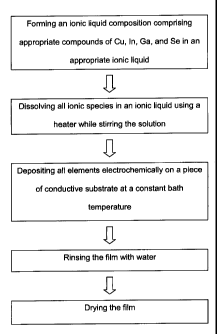
Figure 1 shows a schematic flow chart of the electrodeposition
method according to the present invention;
9
CA 02773709 2012-03-08
WO 2011/029197
PCT/CA2010/001421
Figure 2 is an optical image of a CIGS film formed using the
method of the present invention onto a molybdenum-coated glass taken by
an optical microscope with a 50x lens; and
Table 1 summarizes Examples of CIGS film compositions as a
function of deposition conditions.
DETAILED DESCRIPTION OF THE INVENTION
Generally speaking, the systems described herein are directed to
electrochemical based methods of producing stoichiometric CIGS films
that can be used as absorber layers in solar cells, among other
applications. As required, embodiments of the present invention are
disclosed herein. However, the disclosed embodiments are merely
exemplary, and it should be understood that the invention may be
embodied in many various and alternative forms. The figures are not to
scale and some features may be exaggerated or minimized to show
details of particular elements while related elements may have been
eliminated to prevent obscuring novel aspects.
Therefore, specific structural and functional details disclosed herein
are not to be interpreted as limiting but merely as a basis for the claims
and as a representative basis for teaching one skilled in the art to variously
employ the present invention. For purposes of teaching and not limitation,
the illustrated embodiments are directed to electrochemical based
methods of producing stoichiometric CIGS films for use as absorber layers
in solar cells and II-VI semiconductor films for use as n-type
semiconductor layers to complete the CIGS solar cell production.
CA 02773709 2012-03-08
WO 2011/029197
PCT/CA2010/001421
As used herein, the term "about" or "approximately", when used in
conjunction with ranges of dimensions, temperatures or other physical
properties or characteristics is meant to cover slight variations that may
exist in the upper and lower limits of the ranges of dimensions as to not
exclude embodiments where on average most of the dimensions are
satisfied but where statistically dimensions may exist outside this region.
For example, in embodiments of the present invention dimensions of
components of an apparatus and method of measuring optical properties
of water are given but it will be understood that these are non-limiting.
As used herein, the coordinating conjunction "and/or" is meant to be
a selection between a logical disjunction and a logical conjunction of the
adjacent words, phrases, or clauses. Specifically, the phrase "X and/or Y"
is meant to be interpreted as "one or both of X and Y" wherein X and Y are
any word, phrase, or clause.
As used herein, the phrase "one pot" means fabricating
stoichiometric CIGS film in one-step, i.e., deposition in one
electrochemical bath without any post process such as annealing at high
temperature and/or in selenium atmosphere.
According to the invention, alloy constituent species comprising
stoichiometric ratio of copper, indium, gallium, and selenium are preferably
obtained from an ionic liquid solution of a mixture of compounds
comprising copper, indium, gallium, and selenium with the anions being
any one of sulfate, acetate, bromide, fluoride, chloride, iodide, hydroxide,
nitrate, oxalate, citrate, phosphate, tungstate, hydrates or combinations
thereof.
11
CA 02773709 2012-03-08
WO 2011/029197
PCT/CA2010/001421
In a preferred embodiment of the invention, the liquid composition is
comprised of an ionic liquid mixture of copper (II) chloride, indium (III)
chloride, gallium (III) chloride, and selenium (IV) chloride. Stoichiometric
CIGS films means film compositions close to CulnxGa1_xSe2, with x ranging
from 0.6 to 0.8, which is suitable for CIGS films for use in solar cell
production.
Preferably, the atomic concentrations in the ionic liquid are from
about 5 mM to about 10 mM for copper, from about 40 mM to about 60
mM for indium, from about 40 mM to about 60 mM for gallium, and from
about 60 mM to about 80 mM for selenium. More preferably the atomic
concentrations are from about 6 mM to about 8 mM for copper, from about
40 mM to about 50 mM for indium, from about 40 mM to about 50 mM for
gallium, and from about 65 mM to about 75 mM for selenium.
We have found that it is possible to use different electrochemical
methods such as cyclic voltammetry, constant potential, or constant
current to make stoichiometric CIGS films suitable for solar cell production.
Between these various electrochemical methods, cyclic voltammetry
typically gives superior film morphology because after the potential sweep
for film deposition, the other half-cycle can be engineered to etch off any
undesirable heterogeneous growth features at the growth front. However,
in some applications the constant current method of production may be
preferred based on its faster deposition rate.
In the present invention, it is preferable to use the cyclic
voltammetry technique with the potential from about -0.2 V to about -2.2V,
while it is more preferable to carry out cyclic voltammetry in the potential
12
CA 02773709 2012-03-08
WO 2011/029197
PCT/CA2010/001421
range from about -0.1 V to about -2.0 V. When the constant potential
method is used, it is preferable to use a constant potential more negative
than -1.30 V applied to the working electrode on which the CIGS film is
being deposited, and it is more preferable to use a constant potential of
about -1.35 V. In the constant potential mode for electrodeposition the
potential may be held in a range from about -1.30 V to about -1.60 V.
Thus, in the constant potential mode, a constant potential is applied to the
conductive substrate (which serves as one electrode) and the counter
electrode such that the voltage on the conductive substrate is more
negative than -1.30 V, and it is more preferable to use -1.35 V.
In constant current mode, it is preferred to use current density more
than -1.2 mA/cm2, more preferably between -1.2 mA/cm2and -4.2 mA/cm2.
It will be appreciated that the CIGS films may be deposited onto
numerous types of substrates such as metallic substrates including but not
limited to molybdenum, aluminum, copper, platinum, conductive oxides
including but not limited to indium-tin-oxide-coated-glass, indium-tin-oxide-
coated-polymer, other conductor-coated-insulators, electrically conductive
polymers. More particularly, the substrate may comprise conductive
polymer, polymer coated by metal, polymer coated with a transparent and
conductive layer, ITO on glass, ITO on polymer, ceramic coated with a
conductive layer, metal, amorphous semiconductor materials, crystalline
semiconductor materials, polycrystalline semiconductor materials, or
combinations thereof.
Any ionic liquid may be used as the solvent; however, it is
preferable to use reline, which is a mixture of urea and choline chloride, as
13
CA 02773709 2012-03-08
WO 2011/029197
PCT/CA2010/001421
the solvent. It will be appreciated by those skilled in the art that numerous
other ionic solvents such as any imidazolium- and pyridinium-based ionic
liquids may be used.
In order to achieve electrodeposition, the solution is heated to a
temperature which preferably ranges from 50 C to about 100 C, more
preferably from about 55 C to about 85 C, and most preferably from about
60 C to about 75 C. In all cases, the bath temperature should be kept
constant during the deposition. For example, this can be achieved with a
circulating water bath. The reactions may be carried out in a thermal-
jacketed glass beaker with four Teflon stoppers with an appropriate
amount of solution in a small batch approach. In production, a large bath
can be used.
Thus, during electrochemical deposition the ionic liquid may heated
to a temperature which is in a range from about 50 C to about 100 C and
is held substantially constant while the CulnxGa1,Se2 film is
electrodeposited onto the conductive substrate.
The composition, grain size, thickness, morphology, and electrical
properties of the resultant CIGS films are influenced by the deposition
conditions which include (a) proper bath compositions with the four cations
of CIGS and proper choices of anions, (b) proper choice of ion liquid; (c)
proper bath temperature; (d) proper choice of the substrate electrode and
the pre-deposition treatment of the electrode; (e) proper agitation of the
bath prior to the deposition and during deposition; (f) proper conditions of
applying and sweeping the potential; (g) proper deposition time; and (h)
proper ending of the deposition process. The present invention describes
14
CA 02773709 2012-03-08
WO 2011/029197
PCT/CA2010/001421
the method of one-pot process of depositing stoichiometric CIGS with
grain and electrical properties adequate for solar cell production without
the requirement of post-deposition thermal sintering.
In summary, the present invention is different from the methods
using the aqueous solution approach to deposit CIGS films. In
embodiments of the present invention, precursor compounds comprising
chlorides of Cu, Ga, In, and Se are dissolved in an ionic liquid solution.
The metal cations of the Cu, Ga, In, and Se are then electrochemically
reduced on a molybdenum electrode and the stoichiometric CIGS
semiconductor alloy is formed at the electrode.
Four examples are shown in Table 1 to show the dependence of
film compositions on the conditions of the one-pot ionic-liquid
electrodeposition method. Among these four examples, both Samples #2-
3 have their Se/Cu ratio close to that of a stoichiometric CIGS film suitable
for the production of solar cells. In the course of the development of the
present invention, the inventors have also explored the aqueous solution
approach as a comparative analysis. However, it has been observed that
bath compositions depend on electrodeposition methods and we were
required to adjust it with each method. In addition, the inventors
considered the ratio of In/In+Ga and Cu/In+Ga in making stoichiometric
CIGS films. It was found that in the aqueous solution approach, the
deposition efficiencies of In and Ga are limited by the electro-reduction of
H+ in the aqueous solution. In other words, the electrochemical reduction
of the cations of In, Ga and H are competing in the reduction cycle. In
addition, the formation of hydrogen bubbles during CIGS film deposition
CA 02773709 2012-03-08
WO 2011/029197
PCT/CA2010/001421
also causes undesirable compositional inhomogeneity, surface
morphology and film defects (including pinholes).
The choline chloride/urea eutectic is an appropriate ionic liquid to
prevent these technical problems inherent in the aqueous solution
deposition method because it is stable in air and moisture, and the
operational temperature is conveniently moderate and compatible even
with polymers and other heat-sensitive substrates.
The present method for the electrodeposition of CIGS is different
from the method of L.M. Peter and coworkers (in the publication entitled
"Electrochemical Deposition of CIGS by Means of Room Temperature
Ionic Liquids", Thin Solid Films, 515, 5899-5903 (2007)) in the following
ways:
(a) Peter and coworkers were not able to make stoichiometric CIGS
films using their electrochemical deposition method alone. They used
selenization at 500 C for 30 minutes to form their stoichiometric CIGS
films. In comparison, the present invention uses a one-pot electrochemical
deposition to make stoichiometric CIGS films with no requirement of post-
deposition thermal sintering.
(b) The CIGS growth conditions according to the present invention
are very much different from those used by Peter and coworkers. In the
method of Peter and coworkers, the selenium concentration in the bath
was merely 10mM and when their deposition condition was followed. The
present inventors found CIGS deposits with Cu(ln, Ga)Se0.02. such that Se
was far off its proper concentration in the stoichiometric Cu(ln,Ga)Se2.
16
CA 02773709 2012-03-08
WO 2011/029197
PCT/CA2010/001421
(c) The method of Peter and coworkers only teaches the constant
potential approach of CIGS deposition, whereas the present invention
disclsoses both the constant potential cyclic voltammetry and constant
current approaches can be used. Typically, the cyclic voltammetry method
gives better film morphology than the constant voltage approach. On the
other hand, the constant current deposition method favors shorter
deposition times, which is desirable in industry.
The present invention also teaches the completion of CIGS solar
cell production with each of the p-type CIGS and n-type 11-VI or organic
semiconductor layers deposited by one-pot ionic-liquid electrodeposition.
For the production of solar cells with a buffer layer such as CdS or other
compounds adjacent to the CIGS layer to improve the solar cell efficiency,
the buffer layer is deposited either by a chemical bath method or an
electrodeposition method so that the process is compatible with the
electrodeposition of p-CIGS and n-II-VI layers. In some embodiments,
after the one-pot ionic-liquid electrodeposition of CIGS on a Mo electrode,
ZnO is subsequently deposited also with ionic-liquid electrodeposition. In
one embodiment, stoichiometric CdS is deposited with the chemical bath
method with aqueous solutions of 0.45M cadmium sulfate, 0.15M thiourea,
and 1.8M ammonium at temperatures in a range from about 50 C to about
80 C.
In some embodiments ZnO is deposited with zinc compounds of
acetate, perchlorate, or any other zinc salts. In one embodiment, ZnO is
deposited with 0.1M in reline ionic liquid at 90 C and a constant potential
of -1.5 V. In another embodiement, the cyclic voltammetry with the
17
CA 02773709 2012-03-08
WO 2011/029197
PCT/CA2010/001421
potential sweep from -0.2 to -2.2 V is used. In some embodiemnts, both
CdS and ZnO are deposited with a bath temperature of 65 C.
The present invention is very advantageous for several reasons.
First, the present method can be used to produce stoichiometric CIGS
films suitable for the low-cost and high-throughput production of solar cells
on large surface areas. The electrodeposition can be easily scaled up
with a deposition area >30 m2 with a large bath, and with the option of
automatic feeding of a roll of substrates from one bath to the next bath for
sequential electrodeposition such as the sequential electrodeposition of
CIGS/CdS/ZnO or ZnO/CdS/CIGS. The capital investment and equipment
operating costs of electrodeposition are also much less than those relying
on vacuum technology for deposition or post-deposition treatments. Some
of the electrodeposition processes can also be replaced by simple
chemical-bath processes which are low-cost, scalable, and compatible
with electrodeposition processes.
The present method also allows one to flexibly tune the grain size
for high photo-conversion that results in high conversion efficiency of the
solar cell. The present method thus eliminates the need for any post-
deposition thermal sintering. Most importantly, since the deposition
temperature is typically well below 100 C, the present invention enables
the production of CIGS solar cells on polymer and other heat-sensitive
substrates.
The method disclosed herein will now be exemplified by the
following non-limiting examples that are meant to illustrate and not limit the
method.
18
CA 02773709 2015-09-04
EXAMPLE 1
This example involves electrochemical deposition of copper,
indium, and selenium (CIS) on a substrate which can be any conductive or
senniconductive material such as conductive polymers, metals (sheet), or
deposited metals (such as but not limited to gold, molybdenum, calcium,
vanadium, chromium, silver, cobalt, iron, palladium, aluminum) deposited
on a piece of glass or plastic or something similar. The conditions of this
deposition were: [CuC12} = 7.5 mM, [InCI3]= 65 mM, and [SeCI4] = 40 mM
at 65 C in an ionic liquid at a constant potential of - 1.35 V. It is also
possible to make CIS film using other electrochemical techniques such as
cyclic voltammetry.
While this Example 1 involved deposition of CIS and not CIGS, the
confirmation of the production of stoichiometric CIS films by the present
invention is important because it is the prerequisite of the production of
CIGS films. In addition, CIS can also be used as a practical absorbing
layer in solar cells.
EXAMPLE 2
This example involves electrochemical deposition of CIGS on ITO
glass using an ionic liquid as a solvent where the following concentrations
were used: [CuC12] = 7.5 mM, [InC13] = 55 mM, [GaC13] = 45 mM, [SeC14] =
60 mM. The process was under constant temperature at 65 C for 150
minutes. Cyclic voltammetry was used with the potential range between -
0.1 V and -2.0 V being applied to do the deposition. However, it is possible
to do the stoichiometric deposition using other electrochemical techniques
19
CA 02773709 2012-03-08
WO 2011/029197
PCT/CA2010/001421
such as, but not limited to, applying a constant potential such as was done
in Example 1. Some examples of film compositions are shown in Table 1.
Samples 1-3, particularly Samples 2-3, have film compositions_of Se/Cu
very close to the ideal stoichiometric CIGS composition for solar cell
production. Hence, the deposition conditions of them can be fine-tuned for
the actual solar cell production requirements.
EXAMPLE 3
The method disclosed herein also provides a method for the
fabrication of a solar cell using the CIGS film described in Example 2.
After depositing CIGS film, the edges of the CIGS film were covered, and
CdS and ZnO were electrodeposited in reline at 90 C. For CdS, the
deposition was carried out with aqueous solutions of 0.45M cadmium
sulfate, 0.15M thiourea, and 1.8M ammonium at 80 C in a simple chemical
bath. For ZnO, 0.1M of zinc perchlorite and a constant potential of -1.5V
was used. Then, ITO was deposited on zinc oxide film to complete the
solar cell fabrication.
EXAMPLE 4
The method disclosed herein involves the fabrication of a solar cell
with the procedures and conditions similar to Example 3 except that the
procedures comprise (a) ITO was deposited on a glass substrate, (b) ZnO
was electrodeposited on ITO, (c) CdS was electrodeposited on ZnO, (d)
CIGS was electrodeposited on CdS, and (e) a metal electrode was painted
or electro-deposited on CIGS.
20
CA 02773709 2012-03-08
WO 2011/029197
PCT/CA2010/001421
Table 1 Examples of controlling film compositions of the one-pot
electrodeposited CIGS films
Sample# Bath Composition Film Composition Ga/(Ga
+ In)
[Cu] [In] [Ga] [Se] of the
film
1 7.5 55 50 60 Cul. (Ino.69,
Gao.31)Sei.85 0.31
2 7.5 55 45 60 Cu1.0(Ino.76, Gao.24)Sei.92 0.24
3 7.5 45 45 65 Cuto (Ino.54, Ga0.46)Se2.6 0.46
7.0 50 60 10 Cut() (Ino.so, Gao.40)Seo.02 0.40
[] = mM in the bath composition
* Done under a constant potential of -1.3V and the same condition as
reported by L.M. Peter and coworkers (Thin Solid Films 515 (2007) 5899-
5903).
For Samples #1-3, the choline chloride/urea eutectic was used as
the ionic liquid. The solution was formed by vigorous stirring until a clear
solution was formed but it was not stirred during deposition. The bath
temperature was set at 65 C and cyclic voltammetry from -0.1 V to -2.0 V
(versus a Pt electrode) with a 20 mV/sec scanning rate was applied. The
Mo electrode was pre-etched and rinsed thoroughly prior to the deposition.
The results in Table 1 confirm that the methods of the present
invention can produce CIGS films with a ratio of selenium/copper close to
2.0, which is a technological breakthrough as this has never been
accomplished.
21
CA 02773709 2012-03-08
WO 2011/029197
PCT/CA2010/001421
The present invention is useful for producing multilayer structures
which involves depositing a layer of CulnxGa1_xSe2 on a conductive
substrate with x ranging from 0.6 to 0.8, depositing at least one n-type
semiconductor layer on the CulnõGa1Se2layer, and depositing a top
electrode on the n-type semiconductor layer to form the multilayer
structure.
Alternatively, a layered structure could be produced by depositing at
least one n-type semiconductor layer on a conductive substrate followed
by depositing a layer of CulnõGa1Se2 on the at least one n-type
semiconductor layer with x ranging from 0.6 to 0.8, and thereafter
depositing a top electrode on the CulnGa1_xSe2 layer to form the
multilayer structure.
The at least one n-type semiconductor may be an n-type inorganic
semiconductor or an n-type organic semiconductor. In a preferred
embodiment the n-type inorganic semiconductor layer comprises a
stoichiometric ZnO layer. However it will be appreciated that the n-type
inorganic semiconductor layer may comprise a stoichiometric II-VI
semiconductor layer.
The organic semiconductor may be ITO coated polymer or plastic
(such as polyethylene terephthalate), or fluorine doped ITO deposited on
polymer or plastic such as PET. The ITO coated on polymer or plastic is
forms the back contact for solar cell. As the last step, a front contact is
added to complete the solar cell or optoelectronic device. One of back
contact or front contact should be transparent to let the light pass through
the layers of the device.
22
CA 02773709 2015-09-04
ITO coated on a polymer such as PET may be used as a back
contact onto which is initially deposited an n-type organic/inorganic
semiconductor as the first layer. A non-limiting example of n-type organic
semiconductor is for [6,6]-phenyl-C61-butyric acid methyl ester (PCBM)
which we used for production of a hybrid (n-type organic -p-type inorganic
semiconductor) solar cell.
Other examples of n-type semiconductors that we can be used
include:
[6,6]-Phenyl C61 butyric acid methyl ester
[6,61-Phenyl 071 butyric acid methyl ester
[6,61-Phenyl-C61 butyric acid butyl ester
[6,61-Phenyl-C61 butyric acid octyl ester
[6,6]-Thienyl 061 butyric acid methyl ester
[6,61-Pentadeuterophenyl C61 butyric acid methyl ester
Other examples of organic semiconductors includes derivatives of
fullerene, rylene diimides, derivatives of thiophene, and any combination
thereof.
The CulnõGa1,Se2 layer may have a thickness in a range from
about 100nm to about 5000nm but is not restricted to this range.
The layered structure may include a buffer layer between the
Culn,Ga1_xSe2 layer and the ZnO layer, and this buffer layer may comprise
cadmium sulphide (CdS) or indium selenide (In2Se3). This optional addition
of a CdS buffer layer or similar materials adjacent to the CIGS layer acts to
improve the solar cell efficiency and can be carried out by a chemical-bath
or electrodeposition method which is compatible with this production
23
CA 02773709 2012-03-08
WO 2011/029197
PCT/CA2010/001421
design philosophy of low-cost, large-area, and low-temperature
manufacturing.
The conductive substrate comprises any one of a conductive
polymer, polymer coated by metal, polymer coated with a transparent and
conductive layer, ITO on glass, ITO on polymer, ceramic coated with a
conductive layer, metal, amorphous semiconductor materials, crystalline
semiconductor materials, polycrystalline semiconductor materials, or
combinations thereof.
The multilayer structure may be a solar cell with suitable electrical
contacts contacting the two conductive layers. More generally the
multilayer structure may be an optoelectronic device.
Advantageously all the layers can be deposited in a sequence of
one-pot bath based processes. The present invention provides a method
of electrodeposition of semiconductor layers needed to complete the CIGS
solar cell production with a roll-to-roll substrate feeding mechanism
through a sequence of electrochemical baths.
The present invention is the first demonstration of the production of
CIGS solar cells with the procedures to form the inverted structure of
metal-electrode/p-CIGS/n-11-VI-layers/transparent-electrode/transparent-
substrate in addition to the normal structure of electrode/n-11-VI-layers/p-
CIGS/metal-electrode/substrate.
As used herein, the terms, "comprises" and "comprising" are to be
construed as being inclusive and open ended, and not exclusive.
Specifically, when used in this specification including claims, the terms,
"comprises" and "comprising" and variations thereof mean the specified
24
CA 02773709 2012-03-08
WO 2011/029197
PCT/CA2010/001421
features, steps or components are included. These terms are not to be
interpreted to exclude the presence of other features, steps or
components.
The foregoing description of the preferred embodiments of the
invention has been presented to illustrate the principles of the invention
and not to limit the invention to the particular embodiment illustrated. It is
intended that the scope of the invention be defined by all of the
embodiments encompassed within the following claims and their
equivalents.