Note: Descriptions are shown in the official language in which they were submitted.
CA 02774482 2012-03-16
WO 2010/039108
PCT/US2008/011416
DATA SAMPLING CIRCUIT AND METHOD
FOR CLOCK AND DATA RECOVERY
BACKGROUND OF THE INVENTION
1. Field Of The Invention
The present invention relates to a data communications circuit; and
more particularly, to a circuit and method for clock and data recovery in high
speed digital communications via optical fiber or wire connection.
2. Description Of The Prior Art
Present telecommunications and computer systems require the high
data-rate transmission of digital information between different circuits.
These
circuits may be in close proximity, such as within a single equipment cabinet,
or they may be separated by very long distances. Data may be transmitted
either by electrical impulses carried using a wired connection such as a
coaxial cable or a conductive trace on a circuit board or as light pulses
transmitted through optical fibers. Light pulses are generally generated by
laser diodes (LD's) or light emitting diodes (LED's) and injected into long
fibers of glass or polymeric materials. The fibers are capable of propagating
the light with extremely low losses and acceptably low dispersion, whereby
information embodied in the modulation pattern may be conveyed. The light
that emerges from the other end of the fiber can be detected and reconverted
into electronic signals that reproduce the original signal. In most cases, a
single connection is used in both optical and electrical systems and there is
no
CA 02774482 2012-03-16
WO 2010/039108
PCT/US2008/011416
- 2 -
provision for transmitting a separate clock signal. The increasingly high data
rates now being used in digital systems impose stringent requirements if an
acceptably low bit error rate (BER) is to be attained.
Transmission of digital data, whether done electrically or optically,
generally employs one of two formats: return-to-zero (RZ) format or non-
return-to-zero (NRZ) format. In both formats, a specific time interval is
allocated for each bit. In RZ format, every binary 1 is represented by a full
transition (low¨>high¨>low) between signal levels, and every binary 0
represented by the absence of any pulse transition. In NRZ format, each
binary 1 or 0 bit is represented by a signal level that remains high or low,
respectively, during the bit's entire time period, which is given by the
reciprocal of the data rate. Transitions (high¨low or low¨>high) occur only
when successive bits are different; there are no transitions between two
successive like bits. NRZ format is generally preferred, because it inherently
permits a greater data rate (about double) for a given frequency bandwidth in
the communications channel.
The timing of the bits of digital data transmitted in either RZ or NRZ
format is referenced to a system clock at the origin. The timing ordinarily is
not transmitted downstream using a separate clock signal, so it must be
recovered at the destination in order to properly interpret the received bit
stream. The process of recovering the clock and data is typically termed
clock data recovery (CDR). NRZ format typically presents a greater
difficulty, because fewer transitions are available from which to recover the
clock. Suitable CDR methods are clearly essential for digital communications
CA 02774482 2012-03-16
WO 2010/039108
PCT/US2008/011416
- 3 -
circuits and systems for a wide variety of systems for data transmission,
whether over short distances within a piece of equipment (e.g. communication
with a disk drive of a computer system) or for extended distances for
telecommunications or computer networking.
The problem of clock recovery is particularly challenging in high-
speed, burst mode communications, by which is meant a situation in which a
relatively large amount of information is transmitted during a transmission
interval, followed by a quiescent interval of indeterminate duration. The
desirability of burst-mode transmission arises in many data communications
situations. While certain known CDR circuits function acceptably well with
an extended, if not continuous, data stream, burst-mode transmission presents
far greater difficulties. The timing signal needs to be established quickly as
each burst begins, and it must be re-acquired for each subsequent burst.
Many conventional CDR circuits employ a phase lock loop (PLL)
circuit operating on the incoming data to provide a local clock signal
synchronized to the rate of the incoming data. One such PLL CDR circuit is
depicted by FIG. 1. However, PLL circuits, including that of FIG. 1,
ordinarily require a relatively long time to settle before they are properly
synchronized. Accurate clock recovery and data extraction are only possible
after that synchronization is achieved.
A further difficulty is that the signals encountered in data
communications are not simple sine waves or modulated sine waves, in which
there is substantial harmonic content at the base frequency. Although
synchronized to an underlying clock that is provided at the source and has a
CA 02774482 2012-03-16
WO 2010/039108
PCT/US2008/011416
- 4 -
well-defined base frequency, the data stream is an apparently random signal.
Little of the actual spectral energy density in the data stream is at the base
frequency. Instead, a data stream, particularly one in NRZ format, has a
relatively broadband spectrum, in contrast to the relatively narrow bandwidth
of the data commonly encountered by PLLs in synthesizers, demodulators,
and modulators.
The settling time required for a conventional PLL-based CDR circuit is
frequently accommodated by appending a relatively long header to the
essential data. The header provides enough time for the CDR circuit to settle,
after which it can reliably process the incoming data stream.
The addition of a header of such length has little impact on overall
transmission efficiency for data provided in extended transmissions. On the
other hand, in burst mode, if the required header is an appreciable fraction
of
the overall amount of actual data within each burst, transmission overhead
increases and effective throughput is reduced. In many situations, such as
computer networking, a single communications line is appointed to service
multiple recipients of data from different sources. Over a long time, each
recipient often requires only a small portion of the total available
bandwidth,
but still desires frequent and data-intensive rapid responses for short,
randomly occurring periods. In such instances, it is highly desirable to
minimize the amount of unneeded transmission overhead to maximize the
effective overall capacity of the data line.
One common data transfer protocol using high-speed, burst mode
communications is the GPON system, which operates with a data rate tightly
CA 02774482 2012-03-16
WO 2010/039108
PCT/US2008/011416
- 5 -
controlled to be 1.25 gigabits per second (Gbps). A typical PLL CDR circuit
used with a 1.25 Gbps system requires a time on the order of 25-500 ns to
settle, depending on the particular design of the system used.
As a result of continuing increases in demands for high bandwidth
digital data transmission, especially for burst-mode communications, there
remains a desire and need for improved data communications circuits, notably
including improved clock data recovery circuits.
SUMMARY OF THE INVENTION
In one aspect, the present invention provides a circuit for recovering
clock and data signals from a digital input signal carried in a digital
communications system. Although preferably designed for an input signal
having a preselected data rate of 1.25 Gbps, the circuit in other
implementations operates at other higher or lower data rates. The circuit
comprises: (i) a clock means for generating a recovered clock signal having a
recovered clock frequency synchronized to the appointed data rate; (ii)
initialization means for setting a delay select code signifying a delay
interval
of one of an intermediate, early, or late delay interval, the initialization
means
setting the delay select code to a preselected one of the delay intervals at
the
startup of the circuit; (iii) a data sampling bank receiving the input signal
and
CA 02774482 2012-03-16
WO 2010/039108
PCT/US2008/011416
- 6 -
comprising delay means for delaying the input signal to form delayed signals
in early, intermediate, and late signal channels, the bank being triggered by
the recovered clock; (iv) a pattern detection means for detecting occurrences
of a preselected bit pattern in the input signal and generating a select pulse
in
response to each detection of the preselected bit pattern; (v) a selection
means
connected to the pattern detection means and the data sampling bank and
operative in response to each receipt of the select pulse to update the delay
select code; (vi) a multiplexer receiving the delay select code from the
selection means and signals from the data sampling bank in the early,
intermediate, and late signal channels and outputting an optimum delayed
signal chosen from among the signals in the early, intermediate, and late
signal channels according to the delay select code; and (vii) an output flip-
flop receiving the optimum delayed signal from the multiplexer and being
clocked by the recovered clock signal, the output flip-flop thereby forming
the recovered data signal in synchrony with the recovered clock signal. The
preselected bit pattern consists of a sequence of a preselected initial bit, a
preselected multi-bit timing indication pattern having an indication number of
bits, and a preselected final bit. The updating of the delay select code
preserves the preselected bit pattern in the recovered data signal. The
present
invention also provides a data communications system employing the
foregoing circuit.
Further provided is a method for recovering clock and data signals
from a digital input signal carried in a digital communications system. The
method is preferably implemented in a signal having a preselected data rate of
CA 02774482 2012-03-16
WO 2010/039108
PCT/US2008/011416
- 7 -
1.25 Gbps, but may also be practiced in systems operating at higher or lower
data rates. The method comprises: (i) providing a recovered clock signal
having a recovered clock frequency synchronized to the data rate; (ii)
defining a delay select code signifying a delay interval of one of an
intermediate, early, or late delay interval and initializing the delay select
code
of a preselected one of the delay intervals at the startup of the method;
(iii)
delaying the input signal by each of the early, intermediate, and late delay
intervals to form respective early, intermediate, and late delayed signals;
(iv)
detecting in one of the delayed signals occurrences of a preselected bit
pattern; (v) selecting from among the early, intermediate, and late delayed
signals an optimum delayed signal, the selection being chosen according to
the delay select code; and (vi) retiming the optimum delayed signal to form
the recovered data signal in synchrony with the recovered clock signal. The
preselected bit pattern consists of a sequence of a preselected initial bit, a
preselected multi-bit timing indication pattern having an indication number of
bits, and a preselected final bit. Updating of the delay select code preserves
the preselected bit pattern in the recovered data signal.
The present circuit and method are beneficially employed in a digital
data communications system, particularly one employed for transmitting
information in burst mode at high data rates. The system is readily and
economically implemented. The use of a locally generated clock signal and
alternative, adaptively selected and updated delay times, permits the circuit
to
accurately reconstruct and retime an incoming data stream in synchrony with
a recovered clock. The acquisition of the signal and selection of an
CA 02774482 2012-03-16
WO 2010/039108
PCT/US2008/011416
- 8 -
appropriate delay time are done rapidly, permitting burst-mode signals to be
processed without need for an extended header block that reduces effective
bandwidth.
Preferably, the system is implemented using detection of a bit pattern
consisting of four alternating bits, i.e. a 0101 or 1010 bit pattern.
Detection
of a 0101 sequence is preferred, but the circuit and method may also be
implemented for operation based on the complementary 1010 sequence.
Suitable choice of the delay time permits the circuit and method to
accommodate much larger timing jitter in the incoming data without
unacceptable bit error rates than is possible using existing high data rate
clock
and data recovery circuits adapted for burst-mode applications.
BRIEF DESCRIPTION OF THE DRAWINGS
The invention will be more fully understood and further advantages
will become apparent when reference is had to the following detailed
description of the various embodiments of the invention and the
accompanying drawings, wherein like reference numerals denote similar
elements throughout the several views, and in which:
FIG. 1 is a block schematic diagram showing a prior art CDR circuit
that uses a PLL to recover a clock signal from an incoming digital data
signal;
FIG. 2 is a block schematic diagram showing a prior art CDR circuit
useful in processing burst-mode data at a 1.25 Gbps data rate;
CA 02774482 2012-03-16
WO 2010/039108
PCT/US2008/011416
- 9 -
FIG. 3 is a timing diagram showing digital signals associated with the
circuit of FIG. 2;
FIG. 4 is a schematic depiction of an eye diagram representing
transitions in a digital data stream;
FIG. 5 is a block schematic diagram depicting a CDR circuit of the
present invention;
FIG. 6 is a block schematic diagram system depicting in more detail
the data sampling circuit used in the FIG. 5 circuit;
FIG. 7 is a timing diagram showing digital signals delayed by
processing using the circuit of FIGS. 5-6;
FIG. 8 is a timing diagram showing digital signals delayed by
processing using the circuit of FIGS. 5-6;
FIG. 9 is a timing diagram showing digital signals delayed by
processing using the circuit of FIGS. 5-6;
FIG. 10 is block schematic diagram depicting additional details of the
select logic circuit incorporated in the FIG. 5 circuit;
FIG. 11 is block schematic diagram depicting additional details of the
pattern detection circuit incorporated in the FIG. 5 circuit; and
FIG. 12 is a timing diagram showing digital signals seen in the
operation of the circuit of FIG. 11.
DETAILED DESCRIPTION OF THE INVENTION
CA 02774482 2012-03-16
WO 2010/039108
PCT/US2008/011416
- 10 -
In one aspect of the invention, there is provided a circuit and method
for recovering clock and data signals carried in a digital communications
system to a receiving location. The data may be transmitted by either
electrical or optical techniques. The circuit operates on a digital input
signal
in the form of electrical impulses. When the circuit is used in conjunction
with an optical system, the propagating light pulses are converted using any
converter known in the optical fiber transmission art to provide corresponding
electrical impulses. The circuit may be used for continuous data streams, but
is particularly useful in connection with burst-mode communications.
Referring now to FIG. 2, there is depicted in block diagram form a
known CDR circuit 60 usable for burst-mode communications. The circuit 60
acts to accepts an incoming NRZ-formatted digital signal denoted as data RX,
from which is obtained a regularized, recovered data stream RDATA and a
recovered clock RCLK. The RDATA stream is synchronized to RCLK, by
which is meant that the bit transitions in the data coincide with transitions
in
the RCLK signal. Circuit 60 includes a clock recovery section 59 that
employs three matched, voltage-controlled oscillators. DATA OSC_A 66 and
DATA OSC_B 64 are used in processing the input data, while REF OSC_R 62
is used to generate a well-stabilized, local reference clock OSCCLK having a
frequency matching the input data rate. Typically, specifications require the
locally generated clock rate to match the actual incoming data rate to within
a
few parts per million to ensure satisfactory data recovery.
Clock recovery section 59 provides a reference channel based on a
locally generated reference clock signal REFCLK having a frequency
CA 02774482 2012-03-16
WO 2010/039108
PCT/US2008/011416
- 11 -
subharmonically related to the incoming data rate. A phase lock loop locks
the reference oscillator frequency OSCCLK to a preselected multiple of the
frequency of REFCLK. In the implementation shown, OSCCLK is locked to
1.25 GHz, ten times the frequency of REFCLK (125 MHz). A feedback loop
is established using phase/frequency detection circuit FDET 70 and a lowpass
FILTER 72. FDET 70 compares OSCCLK (divided by 10 by circuit 68) with
REFCLK (running at a local frequency chosen to be one-tenth the base data
rate) to generate an output FDETOUT that is filtered by FILTER 72 to
produce DC bias voltages BIASN and BIASP used to control all three
oscillator circuits. The oscillators must be carefully matched, so that
application of identical input control voltages BIASN and BIASP to all three
oscillators results in outputs at substantially a common frequency. The
matching of the oscillators must be sufficiently close to maintain
synchronization of the recovered clock even in situations in which the
incoming data stream includes long strings of consecutive 0 or 1 bits, during
which there is no opportunity for any adjustment of the respective clocks or
delay times. For example, in some burst-mode applications, the incoming
data may have as many as 72 consecutive 0 or 1 bits in the data stream.
During such a string, generation of the recovered clock relies on one or the
other of DATA OSC_A 66 and DATA OSC_B 64, so that the outputs of these
respective oscillators must remain sufficiently well synchronized to avoid any
timing errors in recovered clock RCLK. This sets stringent limits on the
oscillator matching. Suitable methods are known in the art that permit close
CA 02774482 2012-03-16
WO 2010/039108
PCT/US2008/011416
- 12 -
matching of different sub-circuits during typical integrated circuit
fabrication,
such as by CMOS processing.
In contrast to the conventional PLL-based CDR circuit 1 of FIG. 1, in
which the PLL locks frequency directly to the incoming data, the FIG. 2
circuit 60 locks to a locally generated clock. The operation of the circuit of
FIG. 2 is further made apparent by reference to the timing diagram of FIG. 3.
A typical input signal RX clocks a Divide-by-2 flip-flop circuit 61 to produce
complementary phase signals PHASEA and PHASEB, which respectively
enable DATA OSC_A 66 and DATA OSC_B 64. A rising edge of RX data
(indicated by the arrow "X") turns OSC_A 66 on and turns OSC_B 64 off,
causing OSC_A 66 to generate pulses in the CLKA signal until the next rising
edge of data turns off OSC_A 66 and turns on OSC_B 64, which then
produces CLKB pulses. The propagation delays through the divide-by-two
flip-flop 61 and oscillators 64, 66 produce a delayed rising edge in the CLKA
and CLKB signals, as representatively indicated by arrow "Y." CLKA and
CLKB are OR'ed by gate 74 to produce recovered clock RCLK, which is a
square wave having a frequency corresponding to the bit rate of the RX data
and approximately a 50% duty cycle. A suitably delayed RX signal
(DINDELAY) is input to a D-type flip-flop circuit 78 clocked by RCLK. The
output of flip-flop 78 regularizes the incoming data RX and provides
recovered data RDATA in synchrony with RCLK. The delay time produced
by MATCHING DELAY 76 is selected based on the input data rate and the
typical propagation and switching delays in the various circuits. Preferably,
the delay is chosen so that the flip-flop clocking, based on the falling edge
of
CA 02774482 2012-03-16
WO 2010/039108
PCT/US2008/011416
- 13 -
RCLK, occurs at or near the midpoint of the data period in the DINDELAY
signal. The resulting transitions in recovered data RDATA coincide with
falling edges in recovered clock RCLK, as representatively indicated by arrow
"Z." In the implementation shown, the input data rate is 1.25 Gbps, so each
data bit occupies a period of 800 ps. MATCHING DELAY 76 is preferably
chosen such that the RCLK rising edge occurs at a time nominally about 400
ps after a rising edge in the RX stream, and every 800 ps thereafter.
In the idealized situation depicted by the FIG. 3, the foregoing circuit
and timing provides sampling of the RX signal optimally chosen to be at the
mid-point of each incoming data bit. However, in practice, even signals that
are perfectly formed as rectangular pulses in the transmitter are never
received in pristine condition. Transmission inevitably subjects the pulses to
distortion in both timing and amplitude, so that careful reconstruction of the
original signal must ordinarily be done at the receiving end to assure the
integrity and accuracy of the received data.
Asynchronously transmitted signals are particularly vulnerable to these
distortions. That is to say, the value (0/1) of each incoming bit is assumed
to
be correctly determined by interrogating the data line at a time set at the
receiving end in accordance with a recovered clock provided by the CDR
circuit. If the incoming signal level at that putative interrogation time does
not accurately reflect the intended value, a bit error results.
Time jitter is an especially troublesome source of bit error, particularly
in burst mode transmission. Jitter in digital systems is often represented by
a
CA 02774482 2012-03-16
WO 2010/039108
PCT/US2008/011416
- 14 -
so-called "eye diagram," also known as an "eye pattern," which is a
commonly used representation of the departure of actual digital signals from
ideal form. The eye diagram is generally portrayed as an oscilloscope display
in which a digital data signal from a receiver is repetitively sampled and
applied to the vertical input, while the data rate is used to trigger the
horizontal time sweep. The time base is adjusted to display nominally one bit
period. The name is generally descriptive of the appearance of the resulting
oscilloscope locus. For many commonly used types of coding, the pattern
looks like a series of eyes between a pair of rails.
Referring now to FIG. 4, there is depicted generally at 19 a
prototypical eye diagram. During the nominal time period of each bit, the
signal may be constantly high or low (logical 1 or 0), or it may have a rising
or falling edge, at either the beginning or end of each time slice (or both).
In
particular, the period ideally may include a low¨high--low (0¨>1¨.>0)
transition represented by an initial rising edge 20, a high level 21, and a
final
falling edge 22. Alternatively, there may ideally be a high¨>low¨>high
(1¨>0¨>1) transition with an initial falling edge 24, a low level 25, and a
final
rising edge 26. The slopes of the initial and final edges reflect the rise and
fall times of the digital circuitry. However, in practice, the rising and
falling
edges at both the beginning and end of each period may occur earlier or later
than nominal. Initial rising edge 20 may occur earlier or later, as shown at
20E, 20L. Initial falling edge 24 may also occur earlier or later, at 24E,
24L.
Similarly, advanced or retarded edges may occur at the end of each period,
26E, 26L, 22E, 22L. Any variation from the nominal transition times
CA 02774482 2012-03-16
WO 2010/039108
PCT/US2008/011416
- 15 -
depicted by beginning edges 20, 24 and ending edges 22, 26 represents time
jitter. While FIG. 4 shows only a few transitions for the sake of clarity, it
is
to be understood that an actual data stream would produce an eye diagram
with a dense distribution of jitter times, instead of the single early and
late
transitions shown. Many sources may contribute to jitter, including noise
inherent in an optical transmitter and receiver. Although not shown in the
FIG. 4 diagram, it will also be understood that overshoot/undershoot and
some variation in the amplitude (e.g. voltage or light intensity)
corresponding
to the low and high logic states are also seen, leading to further possible
errors.
Several important system performance measures relating to both signal
amplitude and timing can be derived by analyzing the eye diagram. Signals
that are too long, too short, or poorly synchronized with the system clock, or
have slow high/low transitions are apparent on the left and right sides of the
diagram. Signals that have too high or low amplitude, undershoot/overshoot,
or excessive noise are manifest on the top and bottom of the eye diagram. An
open, substantially rectangular eye pattern corresponds to minimal signal
distortion. Distortion of the signal waveform due to intersymbol interference,
jitter, and amplitude noise all effectively close the eye diagram. For
example,
the prototypical timing variations of the transitions in FIG. 4 narrow the eye
diagram width. Other errors in timing synchronization and jitter critical to
the performance of a CDR circuit are also readily discerned using an eye
diagram.
CA 02774482 2012-03-16
WO 2010/039108
PCT/US2008/011416
- 16 -
In order to extract data reliably using a CDR circuit, sampling must be
done within the opening defined by the locus of the eye diagram
circumscribed by many superimposed transitions, i.e., within the time limit
indicated by arrow "W" of FIG. 4. If sampling is done too early or too late,
it
is almost certain that some bits will be incorrectly represented.
Alternatively
stated, the eye opening defines the amount of jitter allowable in the incoming
data stream without compromising the integrity of the data extracted from the
input.
As noted hereinabove, prior art PLL-based CDR circuits using a PLL
locked to the incoming data stream, such as that shown generally at 1 in FIG.
1, are able to cope with data having relatively large amounts of slowly-
varying jitter. That is to say, the circuit is able to adjust the sampling
point to
accommodate transitions that are significantly earlier or later than nominal,
provided the jitter changes at a rate that is sufficiently low to be
accommodated by the time constant of the filter in the PLL feedback loop.
The FIG. 1 circuit relies on a PLL that locks the frequency of an
internally generated clock directly to the incoming data stream. The PLL is
implemented conventionally using a voltage controlled oscillator 3 driving
phase detector 4 and frequency detector 5 that both operate on the incoming
data signal after it is regenerated through inverter 2. Signals from the
detectors are summed at summer circuit 5 and filtered using low pass filter 6
to close the loop. The PLL thereby provides a recovered clock signal used to
retime the incoming data using flip-flop circuits in retiming circuit 7.
CA 02774482 2012-03-16
WO 2010/039108
PCT/US2008/011416
- 17 -
Typically, the FIG 1 circuit is arranged to provide sampling at the
mid-point of the period of each data bit. For example, in a system used with a
1.25 Gbps data rate, nominal sampling occurs at 400 ps after a bit edge (the
middle of the 800 ps period) and at 800 ps increments thereafter. In some
embodiments, PLL-based CDR circuits can accommodate sampling as early as
100 ps or as late as 700 ps from the nominally expected time of an edge. In
other words, pulses that are as short as 200 ps or as long as 1400 ps may be
accommodated without causing unacceptable bit error rates.
On the other hand, the burst-mode CDR circuit of FIG. 2 relies on a
clock frequency that tracks a locally generated reference source REFCLK
instead of the incoming data signal. The FIG. 2 circuit thus is able to accept
an incoming signal without the need for an extended header to allow for PLL
frequency acquisition, but at the cost of being far less tolerant of timing
jitter.
It is typically found that for an input data rate of 1.25 Gbps, data having a
jitter of more than about 45% (corresponding to a 55% eye opening) cannot
reliably be extracted.
In an aspect of the present invention, there is provided a CDR circuit
that is capable of accurately processing burst-mode data having far more
jitter
than could be tolerated with the circuit of FIG. 2. For example, some
implementations of the present circuit can accommodate jitter characterized
with an eye opening of 30%. Preferably, a circuit, such as circuit 80 depicted
by FIG. 5, permits adaptive selection from among a predetermined nominal,
intermediate sampling time and alternative predetermined earlier or later
sampling times. The additional sampling time options permit a considerable
CA 02774482 2012-03-16
WO 2010/039108
PCT/US2008/011416
- 18 -
amount of jitter to be accommodated. Preferably, the selection of nominal,
early, or late sampling is regularly updated and done automatically and
algorithmically. The present CDR circuit is particularly useful in processing
data in which a preselected data pattern (or signature) recurs frequently.
Each
occurrence of such a data pattern affords an opportunity for determining an
optimal sampling time that preserves, in the recovered and resynchronized
data stream, a preselected bit pattern detected in the incoming data stream.
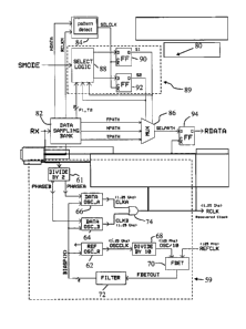
An implementation of a CDR circuit useful in the present system is
depicted generally at 80 in FIG. 5. This circuit includes a clock recovery
section 59 similar to that employed in the FIG. 2 circuit, along with a delay
selection section. One preferred type for the oscillator circuits in clock
recovery section 59 is a current starved oscillator, though other types
providing a suitable voltage-controlled output are also usable. The circuit
depicted is designed for a 1.25 Gbps data rate, so the OSCCLK and RCLK
clock frequencies are commensurate at 1.25 GHz. The REFCLK frequency
can be any frequency which, when multiplied by a preselected integer
multiple, equals the desired OSCCLK frequency. Preferably, the preselected
integer multiple ranges from 4 to 32. More preferably, a multiple of 10 is
used as shown in FIG. 5. Circuit 68 provides division by the preselected
integer multiple. The factor of 10 is conveniently used in implementations in
which the incoming data is in the form of 10-bit words, so that REFCLK
cycle corresponds to the receipt of one word that can be decoded using a
suitable serial to parallel conversion circuit. It will be recognized that in
other implementations, the REFCLK frequency could be chosen to equal the
CA 02774482 2012-03-16
WO 2010/039108
PCT/US2008/011416
- 19 -
base data rate, in which case divisor circuit 68 would be eliminated. SMODE
provides a switch by which the adaptive selection can be disabled for testing
or during operation if desired.
Circuit 80 accepts an input data stream RX, which is sampled at three
different delay times by Data Sampling Bank 82, thereby producing signals in
three different delayed signal channels: nominally delayed intermediate signal
channel NPATH (equivalent to DINDELAY of FIG. 2) and channels FPATH
and TPATH that are respectively delayed by an early delay interval and a late
delay interval.
One implementation of Data Sampling Bank 82 is provided by the
circuit shown in FIG. 6. Input RX is concurrently processed through three
paths to produce corresponding data streams with different amounts of delay.
More specifically, a data stream NDATA is delayed by a nominal,
intermediate delay 96 in channel NPATH, while data streams LDATA and
EDATA are respectively delayed with greater and lesser delays 97, 98 in
channels TPATH and FPATH. The three delays are typically provided by
passing the signals through one or more suitable logic circuits which may be
of any type known in the digital electronics art. It is preferred that the
intermediate, early, and late delay intervals range from about 56 to 144 %,
about 81 to 169 %, and about 31 to 119 % of the time period corresponding
to one bit at said data rate. Other similar delay intervals are suitable for
implementations of the present circuit at other base data rates.
FIGS. 7-9 depict the timing of the signals produced by Data Sampling
Bank 82. Portions of a representative incoming stream are shown delayed
CA 02774482 2012-03-16
WO 2010/039108
PCT/US2008/011416
- 20 -
signals EDATA, NDATA, and LDATA, respectively correspond to the signal
channels FPATH, NPATH, or TPATH. All three signals are referenced to the
timing of recovered clock RCLK. FIG. 7 illustrates the idealized situation
(also shown FIG. 3) in which each of the bits, either 1 or 0, in the incoming
RX signal occupies substantially the full interval established by the data
rate.
By way of contrast, FIGS. 8-9 depict the delayed signals resulting from an
RX data stream bearing the same information as in FIG. 7, but with the data
jittered, producing bits that are "thin" or "fat," respectively. The terms
"thin"
and "fat" are used herein refer to pulses that occupy a portion of the time
interval appointed for each data bit that is narrower or broader than the
normal interval dictated by the nominal data rate.
In the examples shown, which involve a 1.25 Gbps data rate, each bit
nominally occupies an 800 Ps time slice and the sampling times are
referenced to the falling edges of RCLK. Sampling of the idealized signal of
FIG. 7 is optimally done at the midpoint of each bit, that is to say, at a
time
triggered 400 Ps after a rising edge, and at 800 Ps intervals thereafter, as
indicated by the arrows on the falling edges of RCLK. However, the same bit
pattern (binary 1011010010) would result from sampling in any of the
channels. On the other hand, FIG. 8 depicts the results of sampling done on
very "thin" data, i.e. data in which a single bit, positive-going pulse lasts
much less than 400 Ps. It is apparent that sampling done in the intermediate
channel, i.e. with triggering 400 ps after a rising edge, will incorrectly
return
certain bits. In particular, both intermediate and early channels will return
a
binary 0010000000, whereas the late channel will correctly return a binary
CA 02774482 2012-03-16
WO 2010/039108
PCT/US2008/011416
-21-
1011010010. A comparable problem arises with the "fat" pulses in FIG. 9, in
which only the early signal channel returns the correct pattern, whereas the
intermediate and late channels return binary 1111111011. Alternatively
stated, the idealized data of FIG. 7 can be accurately sampled either at the
nominal time (400 ps after the rising edge) or at the earlier or later times
afforded by EDATA or LDATA. However, the thin data of FIG. 8 can be
accurately sampled only in the LDATA channel and the fat data of in FIG. 9
can be accurately sampled only in the EDATA channel.
The delay selection circuit 80 of FIGS. 5-6 largely mitigates or
eliminates errors stemming from inopportune timing of the sampling of
jittered data, thereby accommodating both unjittered data and data with jitter
ranging from thin to fat. In a 1.25 Gbps implementation, data as thin as 250
ps or as fat as 1350 ps can be reliably processed.
In the implementation of FIGS. 5-6, one of the delayed signals is
selected by multiplexer MUX 86 in accordance with a delay select code, such
as a bit pair (S1,S2) cooperatively determined by Select Logic circuit 88 and
Pattern Detector 84, as further described below. In the implementation
shown, selection means 89 comprises Select Logic circuit 88 and flip-flops
90, 92. The selected signal data stream is output from multiplexer 86 as
SELPATH and then synchronized with the recovered clock RCLK using D-
type flip-flop 94 to provide recovered data RDATA.
Select Logic circuit 88 continuously receives data processed from each
path by Data Sampling Bank 82 in the following manner. With reference to
CA 02774482 2012-03-16
WO 2010/039108
PCT/US2008/011416
- 22 -
FIG. 6, Data Sampling Bank 82 includes three channels, each having three D-
type flip-flops sequentially connected in that path; all the flip-flops are
triggered on the negation of RCLK. Each set of flip-flops thus acts as a shift
register to retain a 2-bit sequence of the incoming RX data stream, as delayed
in the respective signal channel. The bit stream includes two sequential bits
in each path, respectively denominated as (N1,N2) in the nominal delay
stream NDATA, (F1,F2) in the lesser delay stream EDATA, and (T1,T2) in
the greater delay stream LDATA. These retained bits are all updated with
each RCLK pulse. In the implementation shown, the greater delay used for
LDATA is provided by sequential passage of the RX signal through matching
delay 96 and extra delay 97. Other delay arrangements are possible. For
example, the NDATA signal might be obtained by sequential passage of the
RX signal through lesser delay 98 and then matching delay 96.
One form of the pattern detect logic suitable for an implementation
based on 0101 sequences in RX is provided by the circuit of FIG. 11. Other
implementations are also possible, and it will be understood that the present
system might also be implemented based on other preselected sequences by
using suitable detection logic.
Referring now to FIG. 11, Pattern Detector 84 operates to sense the
occurrence of a preselected low-high-low-high sequence in the incoming NRZ
data stream and provide a pulse in the SELCLK channel in response.
Preferably, the sequence is sensed in the NDATA data stream. The operation
of Pattern Detector 84 is further revealed by the timing diagram of FIG. 12.
Incoming data NDATA containing randomly-occurring low-high-low-high
CA 02774482 2012-03-16
WO 2010/039108
PCT/US2008/011416
- 23 -
sequences 152 is fed to a monostable pulse generator 140 triggered to produce
a pulse PPULSE on every transition. The PPULSE duration is short
relative to width of pulses in RCLK. SR Latch 142 latches on PPULSE to
produce a corresponding ONEDET pulse, which is caused to have a duration
of one RCLK clock cycle by the reset loop driven by AND gate 148. The
shift register formed by sequential D-type flip-flops 144, 146 produces a one-
cycle ONESIG pulse on the next rising clock edge after the occurrence of a
binary 10 in the data stream. AND gate 150 senses coincidence of ONESIG
and PPULSE, thereby producing a short pulse SELCLK indicative of
detection of the binary sequence 0101 in the incoming data.
The generation of the SELCLK pulse in turn triggers updating of the
delay select code. In the circuit of FIG. 5, the delay select code is
specified
by a bit pair denominated as (S1,S2), in accordance with Table I, wherein N,
L, and E respectively denote the intermediate (nominal), late, and early
signal
channels.
TABLE!
Definition of Delay Select Codes by Bit Pair (S1,S2)
S1 S2 Delay
X 0 N
0 1 L
1 1
In particular, the SELCLK pulse triggers flip-flops 90 and 92, thereby causing
the old (S1,S2) bit pair to be updated to values then being determined by
Select Logic 88. The new (S1,S2) values encode the updated delay select
CA 02774482 2012-03-16
WO 2010/039108
PCT/US2008/011416
- 24 -
code controlling MUX 86 until updating at the next occurrence of the
preselected bit sequence.
In an implementation of the present method based on detection of an
0101 bit sequence in the incoming data stream, the updating of the delay
select code is done based on the current delay select code, along with the
first
sample bit in the early signal channel (F1), and the second sample bit in the
late signal channel (T2). The updating is done in accordance with the logic
specified by Table II.
TABLE II
Logic Table for Updated Delay Select Code)
Fl T2 Old New
Delay Delay
0 0
0 0
0 0
1 1
1 1
1 1
1 0
1 0
1 0
It is found that the other possible combination (F1=0 and T2=1),
although logically possible, does not arise in practice in coincidence with
the
detection of a 0101 sequence, except in the case of extremely large jitter
beyond the limits of what the present circuit and method can reliably
accommodate. As a result, updating of delay time in the F1=0/T2=1 instance
ordinarily is not effectual.
=
CA 02774482 2014-05-07
-25-
With reference to FIG. 10. selection means 89. including Select Logic
Circuit 88, operates in accordance with the full logic set forth in Table III
below,
with the possible cases being labeled as shown. Circuit 88 includes NOT gates
(inverters) 110. 112 and 114. Circuit 88 includes NAND gates 116, 118. 120,
122.
124 and 126. Table Ill provides one possible implementation of the logic of
Table
II that is appropriate for the foregoing low-high-low-high (0101) preselected
sequence. Circuit 88 thus determines algorithmically if selection of a
different one
of the delay times would improve the likelihood of accurate data recovery.
TABLE III
(Logic Table for Select Logic 88)
Case El T2 Old SI Old S2 Old New SI New S2 New
Delay Delay
A 0 0 0 0 N 0 1 L
B 0 0 0 I 1, 0 1 L
C 0 0 1 0 N 0 1 L
D 0 0 1 I E 0 0 N
E 0 1 0 0 N 1 1 E
F 0 1 0 1 L 0 1 L
G 0 1 1 0 N 1 1 E
H - 0 1 1 1 E 1 1 E
I 1 0 0 0 N 0 0 N
J 1 0 0 1 L 0 0 N
K 1 0 1 0 N 0 0 N
L. I 0 1 1 E 0 0 N
M 1 1 0 0 N 1 I F
N I 1 0 1 L 0 0 N
O I 1 1 0 ' N 1 1 E
P 1 1 1 1 E 1 1 E
More speci heal ly. the functioning of Select Logic 88 in a preferred
embodiment relies on the particular effect jitter has on the behavior of the
El and
12 bits. As set forth above, these bits are retained at each RCLK cycle by
CA 02774482 2012-03-16
WO 2010/039108
PCT/US2008/011416
- 26 -
Data Sampling Bank 82 from the FPATH and TPATH channels, respectively,
and processed through Select Logic Circuit 88. The CDR circuit of FIGS. 5-
6 is initially set to use the nominal delay of NPATH, but at every occurrence
of the preselected 0101 sequence in the received data stream RX, the
SELCLK pulse causes the optimum selection of delay from among NPATH,
FPATH, and TPATH to be updated and maintained until the occurrence of the
next preselected sequence. The initialization of the delay setting can be
accomplished in any suitable way. For example, a master reset can be applied
during quiescent periods during which no data is being sent. Alternatively, a
short header of data (preferably a 1010101010 sequence) that ensures
availability of numerous bit patterns on which the present CDR circuit can
operate may be included.
The current delay selection setting is encoded in (S1,S2) and the
instantaneous values of the Fl and T2 bits are input to Select Logic circuit
88,
which continuously calculates candidate new values of Si and S2. Upon
receipt of a SELCLK pulse signaling the presence of a binary "10" sequence
in the RX data stream, D-type flip-flops 90, 92 update the current setting of
Si and S2 to the candidate values. The updated (S1,S2) data pair in turn
drive the subsequent selection of a delayed signal channel by multiplexer
MUX 86.
In particular, Fl represents the earliest possible detection of the first
bit of a preselected, timing indication pattern having two timing indication
bits, while T2 represents the latest possible detection of the second bit of
the
pattern. The Fl and T2 bits are tested at each occurrence of a SELCLK pulse
CA 02774482 2012-03-16
WO 2010/039108
PCT/US2008/011416
- 27 -
indicating that the preselected sequence has come in the RX data stream.
Under ideal, non-jittered conditions, two-bit sequences in any of the paths
NPATH, TPATH, OR FPATH could be sampled at the SELCLK pulse and
would yield the desired timing indication pattern, although NPATH is
ordinarily selected. At any given triggering, detection of a "10" in all three
paths indicates NPATH is optimal. If NPATH is already selected, it remains
so (Cases I, K); TPATH is switched to NPATH (Cases J, N); FPATH is
switched to NPATH (Cases D, L). If the data pulses begin to grow thinner,
then fat path bit Fl will first fail to detect a "1" in coincidence with a
binary
"10" detection, indicating warrant for a switch from nominal path NPATH to
the thin path TPATH (Cases A, C). On the other hand, if the data grow fatter,
the thin path bit T2 will be the first to fail to detect a "0" in coincidence
with
a "10" detection, initiating a switch from nominal path NPATH to the fat path
FPATH (Cases M, 0).
Still referring to Table III, Cases H, P are situations in which selection
of fat path FPATH remains optimal as long as bit T2 remains a "1."
Thereafter, a thinning of formerly fat data pulses is first signaled by a
detection of a "0" in T2 in coincidence with a binary "10" pattern, initiating
a
switch from FPATH to normal path NPATH (Cases D, L). On the other hand,
continuing selection of thin path TPATH remains optimal as long as bit F!
remains a "0" (Cases B, F). A widening of formerly thin data pulses is first
signaled by a detection of a "1" in Fl in coincidence with a binary "10"
pattern, initiating a switch from thin path TPATH to NPATH (Cases J, N).
CA 02774482 2014-05-07
-28-
Although implemented in the logic of circuit 88. cases E and G ordinarily do
not
arise in actual data, absent anomalously large jitter.
Preferably, any change to the optimal delay time is initiated only at the
occurrence of a SELCLK pulse and is thus made seamlessly. That is to say, no
bit
error is produced in recovered data as a result of the change in delayed
signal
channel.
Other implementations of the selection means might rely on some more or
all of bit pairs (FI,F2), (NI .N2). and (TI .T2) in the incoming data streams.
The present system is preferably implemented for processing data
encoded in 8B1OB format. Generally stated, 8B10B is an encoding that maps 8-
bit
symbols onto 10-bit symbols to achieve DC-balance and bounded disparity. The
redundancy afforded by the extra two bits assures that state changes occur
with
sufficient frequency to facilitate clock recovery. In particular, the encoding
insures that there are just as many "1"s as "0"s in a string of two 10-bit
symbols,
and that there are not too many sequential "I 's or "0"s. As a result,
level
transitions (1--40 and 0¨>1) and certain data patterns, notably including bit
patterns
with four alternating bits (i.e., "0101" and "1010-) occur frequently. One
implementation of 8BIOB encoding is provided by US Patent 4.486.739 to
Franaszek et al.
It will be understood that the present circuit and method may also be used
in conjunction with other forms of binary data encoding. Preferably an
encoding is
used that results in frequent occurrence of particular bit patterns.
CA 02774482 2014-05-07
-29-
More preferably. a pattern having a sequence of single alternating bits is
frequent. A
particularly preferred pattern that provides one implementation of the present
method is a
binary "0101 sequence. It will be understood that by inverting the logic, the
present method
and circuit could be implemented similarly based on a "1010" sequence. More
preferably, a
"0101" sequence occurs frequently in the data stream. For example each binary
"0101"
sequence includes the aforementioned "10" pattern with a preceding "0" and a
trailing "1." In
a preferred implementation, the frequent occurrence of such binary "10"
patterns permits the
optimal delay time to be ascertained and updated rapidly in response to
changing jitter.
The scope of the claims should not be limited by the preferred embodiments set
forth
above, but should be given the broadest interpretation consistent with the
description as a
whole.