Note: Descriptions are shown in the official language in which they were submitted.
CA 02774970 2014-10-30
=
BALLAST CIRCUIT FOR LED-BASED LAMP INCLUDING POWER FACTOR
CORRECTION WITH PROTECTIVE ISOLATION
[0001]
TECHNICAL FIELD
[0002] The present application relates to a ballast circuit for a light
emitting diode (LED)-based
lamp including power factor correction with protective isolation.
BACKGROUND
[0003] The development of high-brightness LEDs has led to use of such devices
in various lighting
fixtures. In general, an LED-based lamp operates in a fundamentally different
way than an
incandescent, or gas discharge lamp, and therefore may not be connectable to
existing lighting
fixtures designed for those types of lamps. A ballast circuit may be used,
however, to allow use of an
LED-based lamp as a retro-fit for existing lighting fixtures.
[0004] The ballast circuitry for an LED-based lamp generally converts an
alternating current (AC)
input, such as a 120V/60Hz line input or input from a dimmer switch, to a
stable direct current (DC)
voltage used for driving the LED-based lamp. Such circuitry may incorporate a
rectifier for
receiving the AC input and a DC-DC converter circuit. The DC-DC converter
circuit may receive an
unregulated DC output from the rectifier and provide a stable, regulated DC
output to the LED-
based lamp.
[0005] A variety of DC-DC converter configurations are well-known in the art.
Certain types of
known DC-DC converter configurations, such as buck converters, boost
converters, buck-boost
converters, etc., are generally categorized as switching regulators. These
devices include a
switch, e.g. a transistor, which is selectively operated to allow energy to be
stored in an energy
storage device, e.g. an inductor, and then transferred to one or more filter
capacitors. The filter
capacitor(s) provide a relatively smooth DC output voltage to the load and
provide essentially
continuous energy to the load between energy storage cycles.
[0006] One issue with such switching regulator configurations is that there
may be no protective
isolation between the unregulated DC voltage and the regulated DC output
voltage.
1
CA 02774970 2012-03-21
WO 2011/059578 PCT/US2010/050294
In some configurations, the unregulated DC voltage may be 400 Volts or more.
The
unregulated DC voltage can be dangerous if inadvertently applied to the load.
[0007] To provide protective isolation, therefore, a transformer-based
switching regulator,
such as a known "flyback" converter, may be used. In a transformer-based
switching
regulator, the primary side of the transformer may be coupled to the
unregulated DC voltage.
The regulated DC output voltage is provided at the secondary side of the
transformer, which
is electrically isolated from the primary side of the transformer. The
transformer may thus
provide protective isolation of the DC output from the unregulated DC voltage.
[0008] Another issue with switching regulator configurations is that they
involve a pulsed
current draw from the AC power source in a manner that results in less than
optimum power
factor. The power factor of a system is defined as the ratio of the real power
flowing to the
load to the apparent power, and is a number between 0 and 1 (or expressed as a
percentage,
e.g. 0.5 pf = 50% pf). Real power is the actual power drawn by the load.
Apparent power is
the product of the current and voltage applied to the load.
[0009] For systems with purely resistive loads, the voltage and current
waveforms are in
phase, changing polarity at the same instant in each cycle. Such systems have
a power factor
of 1.0, which is referred to as "unity power factor." Where reactive loads are
present, such as
with loads including capacitors, inductors, or transformers, energy storage in
the load results
in a time difference between the current and voltage waveforms. This stored
energy returns
to the source and is not available to do work at the load. Systems with
reactive loads often
have less than unity power factor. A circuit with a low power factor will use
higher currents
to transfer a given quantity of real power than a circuit with a high power
factor.
[0010] To provide improved power factor, some lamp ballast circuit
configurations are
provided with a power factor correction circuit. The power factor correction
circuit may be
used, for example, as a controller for controlling operation of the transistor
switch in a DC-
DC converter configuration such as a "flyback" converter. In such a
configuration, a power
factor controller may monitor the rectified AC voltage, the current drawn by
the load, and the
output voltage to the load, and provide an output control signal to the
transistor to switch
current to the load having a waveform that substantially matches and is in
phase with the
rectified AC voltage.
2
CA 02774970 2012-03-21
WO 2011/059578 PCT/US2010/050294
SUMMARY
[0011] In conventional lamp ballast configurations including a transformer-
based switching
regulator and power factor controller circuits, such as those described above,
complete
isolation between the primary and secondary sides of the transformer has been
sacrificed to
provide a feedback to the power factor controller or, for example, to
establish a common
ground path for the circuit. This, however, increases the potential risk
associated with
inadvertent application of the unregulated DC voltage to the load. In
addition, when such
configurations are used with conventional phase-control dimming circuits, the
transient
response time associated with the power controller circuit may not be
sufficient to establish
acceptable dimming of the lamp without perceptible flicker.
[0012] Consistent with the present disclosure, therefore, there is provided an
LED ballast
circuit and system that converts AC input such as a 120V/60Hz input into a
current source for
an LED-based light source. The circuit includes complete transformer isolation
and may use
a single integrated circuit power factor controller to produce a pulsating DC
output current
that is amplitude modulated by the power factor controller at, for example,
120 Hertz. The
resulting input power factor may be set very close to unity. The total
harmonic distortion at
the input may be very low, and any conducted EMI may be mitigated by the
variable
frequency switching technique. Additionally, the size of the transformer may
be relatively
small because of the high frequency operation and the switching topology, and
the controller
bias network and feedback configuration may eliminate the need for large
electrolytic
capacitors, or multiple capacitors, for dimming applications. The circuit may
thus provide a
very high power factor, high efficiency and small size that will work with
dimmer switches,
such as a reverse phase FET dimmer, without flicker at small conduction
angles.
[0013] In an embodiment there is provided a ballast circuit to drive a light
emitting diode
(LED)-based light source. The ballast circuit includes a rectifier circuit
configured to receive
an AC input voltage and provide an unregulated DC voltage, and a transformer.
The
transformer has a primary winding coupled to the rectifier circuit, at least
one secondary
winding configured to be coupled to the LED-based light source, and a feedback
winding, the
secondary winding being electrically isolated from the primary winding and the
feedback
winding with no electrical path between the primary winding and the secondary
winding or
the feedback winding and the secondary winding. The ballast circuit also
includes a switch,
the switch being configured to close to couple a portion of the unregulated DC
voltage across
the primary winding and the switch being configured to open to transfer energy
from the
3
CA 02774970 2013-11-22
=
primary winding to the secondary winding to provide a DC output voltage to
drive the LED-
based light source. The ballast circuit also includes a power factor
correction circuit
configured to control the switch in response to a first signal representative
of current through
the primary winding, a second signal representative of current through the
feedback winding,
and a third signal representative of the unregulated DC voltage, with no
feedback signal
coupled from the secondary winding to the power factor correction circuit.
[0014] In a related embodiment, the ballast circuit may further include a
switched bias
circuit, the switched bias circuit including a bias circuit switch configured
to close when the
switch is open to provide a supply voltage to the power factor correction
circuit. In a further
related embodiment, the switched bias circuit may be coupled to the feedback
winding, and
the bias circuit switch may be configured to close in response to current
through the feedback
winding.
[0015] In another related embodiment, the ballast circuit may further include
an over-voltage
protection circuit coupled to the power factor correction circuit to disable
the power factor
controller circuit when a voltage at the transformer exceeds a predetermined
level. In a
further related embodiment, the over-voltage protection circuit may include a
Zener diode
coupled to the feedback winding, whereby a breakdown voltage of the Zener
diode is
exceeded when the voltage at the transformer exceeds the predetermined level
thereby
disabling the power factor controller circuit. In another further related
embodiment, the over-
voltage protection circuit may include an over-voltage protection switch
configured to close
when the voltage at the transformer exceeds the predetermined level thereby
disabling the
power factor controller circuit.
[0016] In still another related embodiment, the power factor correction
circuit may include an
integrated circuit power factor controller configured to receive the first
signal, the second
signal, and the third signal and to provide an output to control the switch.
In yet another
related embodiment, the AC input signal may be a 120V AC signal.
[0017] In another embodiment, there is provided an LED-based lamp assembly.
The LED-
based lamp assembly includes a lamp housing, a light source disposed within
the lamp
housing, and a ballast disposed within the lamp housing. The ballast includes:
a rectifier
circuit configured to receive an AC input voltage and provide an unregulated
DC voltage; a
transformer having a primary winding coupled to the rectifier circuit, at
least one secondary
winding coupled to the LED-based light source, and a feedback winding, the
secondary
winding being electrically isolated from the primary winding and the feedback
winding with
no electrical path between the primary winding and the secondary winding or
the feedback
4
CA 02774970 2013-11-22
winding and the secondary winding; a switch, the switch being configured to
close to couple
a portion of the unregulated DC voltage across the primary winding and the
switch being
configured to open to transfer energy from the primary winding to the
secondary winding to
provide a DC output voltage to drive the LED-based light source; and a power
factor
correction circuit configured to control the switch in response to a first
signal representative
of current through the primary winding, a second signal representative of
current through the
feedback winding and a third signal representative of the unregulated DC
voltage, with no
feedback signal coupled from the secondary winding to the power factor
correction circuit.
[0018] In yet another embodiment, there is provided a method of driving an LED-
based light
source. The method includes: receiving an AC input signal, and converting the
AC input
signal into a regulated DC output using a ballast circuit. The ballast circuit
includes: a
transformer having a primary winding, a secondary winding and a feedback
winding, the
secondary winding being electrically isolated from the primary winding and the
feedback
winding with no electrical path between the primary winding and the secondary
winding or
the feedback winding and the secondary winding, and a power factor correction
circuit
receiving no feedback signal coupled from the secondary winding. The method
also includes
coupling the regulated DC output to the LED-based light source.
BRIEF DESCRIPTION OF THE DRAWINGS
[0019] The foregoing and other objects, features and advantages disclosed
herein will be
apparent from the following description of particular embodiments disclosed
herein, as
illustrated in the accompanying drawings in which like reference characters
refer to the same
parts throughout the different views. The drawings are not necessarily to
scale, emphasis
instead being placed upon illustrating the principles disclosed herein.
[0020] FIG. 1 shows a block diagram of a system including an optional dimmer
circuit and
an LED-based lamp assembly according to embodiments disclosed herein.
[0021] FIG. 2 illustrates a block diagram of an LED ballast circuit according
to embodiments
disclosed herein.
[0022] FIG. 3 is a circuit diagram of an LED ballast circuit according to
embodiments
disclosed herein.
[0023] FIG. 4 is a circuit diagram of another LED ballast circuit according to
embodiments
disclosed herein.
[0024] FIG. 5 is a flow diagram of a method according to embodiments disclosed
herein.
CA 02774970 2012-03-21
WO 2011/059578 PCT/US2010/050294
DETAILED DESCRIPTION
[0025] FIG. 1 is a simplified block diagram of one exemplary embodiment of a
system 100
consistent with the present disclosure. In general, the system includes a
light emitting diode
(LED) ballast circuit 102 consistent with the present disclosure for receiving
an alternating
current (AC) input ACin, either directly or through a known dimmer circuit
104, and
providing a regulated direct current (DC) output DCout for driving an LED-
based light
source106. The LED-based light source 106 may be a single LED or multiple LEDs
interconnected in series and/or parallel configurations. In one embodiment, AC
in may be a
provided directly from a 120VAC/60Hz line source. It is to be understood,
however, that a
system consistent with the present application may operate from AC sources,
such as a 220-
240 VAC at 50-60Hz. In an embodiment including a dimmer circuit 104, the
dimmer circuit
may be any known dimmer circuit configuration, such as a reverse phase control
dimmer
circuit. The configuration and operation of such dimmer circuits are well-
known in the art.
[0026] The LED ballast circuit 102 may convert the AC input voltage ACH, to a
regulated DC
output voltage DCout with a high power factor, high efficiency, small size and
protective
isolation. The LED ballast circuit 102 and the LED-based light source 106 may
thus be
provided within a single lamp housing 108, such as within the housing of a
parabolic
aluminized reflector (PAR) lamp, to provide a LED-based lamp assembly 110
consistent with
the present disclosure. The LED-based lamp assembly 110 provides a convenient
retro-fit for
existing lighting fixtures configured to energize PAR lamps including non-LED
based light
sources, e.g. fluorescent or gas-discharge sources. An LED-based lamp assembly
110
consistent with the present disclosure may be inserted directly into such a
lighting fixture to
operate on the AC input thereto, and may operate with a known dimmer circuit.
A lamp
including an LED-based light source 106 may provide long life and low power
consumption
compared to those including non-LED-based light sources.
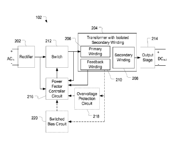
[0027] FIG. 2 is a block diagram that conceptually illustrates the
functionality of an LED
ballast circuit 102 consistent with the present disclosure. As shown, an LED
ballast circuit
102 consistent with the present disclosure may include a rectifier 202, a
transformer 204
including a primary winding 206, secondary winding 208 and a feedback winding
210, a
switch 212 for coupling the output of the rectifier 202 to the primary winding
206 of the
transformer 204, an output stage 214 coupled to a secondary winding 208 of the
transformer,
and a power factor controller circuit 216. The ballast circuit may also
include an over-
6
CA 02774970 2012-03-21
WO 2011/059578 PCT/US2010/050294
voltage protection circuit 218 and/or a switched bias circuit 220. The term
"coupled" as used
herein refers to any connection, coupling, link or the like by which signals
carried by one
system element are imparted to the "coupled" element. Such "coupled" devices,
or signals
and devices, are not necessarily directly connected to one another and may be
separated by
intermediate components or devices that may manipulate or modify such signals.
[0028] In general, the AC input voltage AC., may be coupled to the rectifier
circuit 202,
either directly or through a dimmer circuit 104. The rectifier circuit 202 may
be configured
to rectify AC., to provide an unregulated DC output voltage, i.e. a DC output
voltage that
follows instantaneous variations in the AC input voltage. A variety of
rectifier circuit
configurations are well-known in the art. In one embodiment, for example, the
rectifier
circuit 202 may include a known bridge rectifier.
[0029] The output of the rectifier 202 may be coupled to the primary winding
206 of the
transformer through the switch 212 under the control of the power factor
controller circuit
216. The switch 212 may be a known transistor switch, as is commonly used in
known
switching regulator configurations. In general, when the switch 212 is
"closed", the primary
winding 206 of the transformer 204 is coupled to the output of the rectifier
202 and the
energy is stored in transformer windings. When the switch is "open", the
energy stored in the
secondary winding 208 is coupled to the output stage 214. The output stage 214
may include
a capacitor that is charged by the energy from the secondary winding 208 and
discharges
through the LED-based light source 106 to drive the light source.
[0030] The power factor controller circuit 216 may include a known power
factor controller
(not shown) configured to provide an output to the switch 212 for controlling
the switch 212
in response to a signal representative of current through the primary winding
206, a second
signal representative of current through the feedback winding 210, and a third
signal
representative of the unregulated DC voltage, with no feedback signal coupled
from the
secondary winding 208 to the controller. The output from the power controller
may control
the switch so that the current to the LED-based light source 106 has a
waveform that
substantially matches and is in phase with the output of the rectifier 202,
thereby providing
high power factor.
[0031] Known power factor controllers useful in an LED ballast configuration
consistent
with the present disclosure include known integrated circuit power factor
correction
controllers, such as model number L6561 and L6562 controllers presently
available from ST
Microelectronics of Sunnyvale, CA. The L6561 and L6563 controllers may, for
example, be
employed as a controller in a "flyback" DC-DC converter implementation.
Details of this
7
CA 02774970 2014-10-30
and related alternative applications of the L6561 controller are discussed in
ST
Microelectronics Application Note AN1060, "Flyback Converters with the L6561
PFC
Controller," by C. Adragna and G. Garravarik, January 2003, and ST
Microelectronics
Application Note AN1059, "Design Equations of High-Power-Factor Flyback
Converters based
on the L6561," by Claudio Adragna, September 2003, each of which is available
at
http://www.st.com. Specifically, Application Notes AN1059 and AN1060 discuss
one
exemplary configuration for an L6561-based flyback converter (High-PF flyback
configuration)
that operates in transition mode and exploits the ability of the L6561
controller to perform
power factor correction, thereby providing a high power factor single
switching stage DC-DC
converter. Differences between the L6561 and L6562 controllers are discussed
in ST
Microelectronics Application Note AN1757, "Switching from the L6561 to the
L6562," by
Luca Salati, April 2004, also available at http://www.st.com. For purposes of
the present
disclosure, these two controllers may be discussed as having similar
functionality.
[0032] In a ballast 102 consistent with the present disclosure, the secondary
winding 208 of the
transformer is not electrically coupled in any way to the primary 206 or
feedback winding 210,
e.g. there is no common ground electrical path for the windings and there is
no feedback path
coupled from the secondary winding 208 to the power factor controller circuit
216 or any other
element on primary winding side of the ballast. The power factor controller
operates using
signals coupled thereto from the output of the rectifier 202, and the primary
206 and feedback
windings 210, but no feedback signal is coupled, e.g. electrically or
optically, from the secondary
winding 208 to the controller. This provides complete protective isolation for
the high voltages
on the primary winding side of the transformer and the secondary side of the
transformer. In
addition, by not requiring feedback from the secondary winding 208, the
overall size and
complexity of the ballast is reduced compared to configurations wherein, for
example, optically
isolated feedback is provided from the secondary winding 208 to the
controller.
[0033] As is known, the supply voltage for operating a power factor controller
may be self-
supplied in the ballast configuration to ensure a regulated, stable supply to
the circuit during
operation. In a ballast configuration consistent with the present disclosure
including the
optional switched bias circuit 220, the switched bias circuit 220 may
establish a supply voltage
to the controller with low transient response time and low power dissipation.
In the illustrated
embodiment, the switched bias circuit 220 is coupled between the feedback
winding 210 and
the power factor correction circuit 216. In an embodiment including a
8
CA 02774970 2012-03-21
WO 2011/059578 PCT/US2010/050294
L6561 or L6562 power controller, for example, the switched bias circuit may be
coupled to
the Vcc input of the power factor controller and may include a transistor
switch that turns on
when the switch 212 is opened to use energy transferred from the feedback
winding 210 for
providing a voltage supply to the power factor controller. Such a
configuration provides
rapid transient response that may be particularly useful when the system is
implemented with
a dimmer circuit 104, such as a phased controlled dimmer circuit.
[0034] The optional over-voltage protection circuit 218 may be provided to
shut down or
prohibit operation of the power factor controller circuit 216 upon the
occurrence of an over-
voltage condition. For example, if the LED-based load 106 ceases conducting
current from
the secondary winding 208, e.g. if the load is not connected or malfunctions,
a dangerous
over-voltage condition on the terminals of the transformer 204 may arise. In
the illustrated
embodiment, the over-voltage protection circuit 218 is coupled between the
feedback
winding 210 and the power factor correction circuit 216. In an embodiment
including a
L6561 or L6562 power controller for example, the over-voltage protection
circuit 218 may be
coupled to the NV or ZCD input of the power factor controller for shutting the
controller
down if an over-voltage condition exists.
[0035] The optional switched bias circuit 220 and over-voltage protection
circuit 218 are
described herein as being useful in connection with a ballast wherein the
secondary winding
is completely isolated from the primary and feedback windings and no feedback
is coupled
from the secondary winding to the power factor controller. Those of ordinary
skill in the art
will recognize, however, that these circuits 218, 220 may be provided in a
wide variety of
ballast configurations. For example, these circuits may be included in a
ballast configuration
including different transformer or feedback configuration.
[0036] FIG. 3 is a schematic diagram illustrating one exemplary embodiment of
an LED
ballast circuit 102a consistent with the present disclosure. The illustrated
exemplary
embodiment includes a rectifier circuit 202a, a transformer 204a including a
primary winding
206a, a secondary winding 208a and a feedback winding 210a, a switch Q2 (212a)
for
coupling the output of the rectifier circuit 202a to the primary winding 206a
of the
transformer 204a, an output stage 214a coupled to a secondary winding 208a of
the
transformer 204a, a power factor controller circuit 216a, an over-voltage
protection circuit
218a, and a switched bias circuit 220a. The power factor controller circuit
216a includes an
L6561 integrated circuit power factor controller Ul, the operation of which is
known and
described in ST Microelectronics Application Notes AN1060 and AN1059, referred
to above.
9
CA 02774970 2012-03-21
WO 2011/059578 PCT/US2010/050294
Those of ordinary skill in the art will recognize, however, that other known
power factor
controllers may be used in place of the L6561 controller shown in FIG. 3.
[0037] In operation, the AC input to the circuit AC., is coupled to the
rectifier circuit 202a,
which includes a known bridge rectifier. The rectifier full-wave rectifies the
AC input to
provide a rectified unregulated DC voltage DCin. The output of the rectifier
DC., is
connected to Li and Cl, which filter noise generated in the circuit.
[0038] The primary winding 206a of the transformer 204a is coupled between the
output of
the rectifier circuit 202a and the drain of Q1 so that when Q1 is conducting,
i.e. the switch is
closed, current flows from the output of the rectifier circuit 202a through
the primary winding
206a to energize the primary winding 206a, but when Q1 is not conducting, i.e.
the switch is
open, essentially no current flows through the primary winding 206a. In
general, when the
switch Q1 is closed, the windings of the transformer 204a are energized, and
when the switch
Q1 opens, the polarity of the voltage across the secondary winding 208a and
the feedback
winding 210a reverses to forward bias diodes D3 and D5. When diode D3 is
forward biased,
energy from the secondary winding 208a charges capacitor C4, which is
configured to
discharge through the load when the switch Q1 is open.
[0039] In general, the power factor controller Ul uses a voltage
representative of the output
of the rectifier circuit 202a (i.e., DC.) as a reference to control the level
at which the
controller Ul switches the switch Q1 on and off using a gate drive GD output
coupled to the
gate of Q1 through Rl. This feature allows for a very high power factor
ballast. The
switching frequency is determined by feedback from the primary winding 206a
and the
feedback winding 210a.
[0040] In particular, a portion of DC., is coupled to the multiplier input
MULT of the
controller Ul to provide a signal to the controller Ul representative of the
unregulated DC
voltage DCin. The MULT input is coupled between R2 and the parallel
combination of R3
and C5. Selection of R3 and C5 allows for a tradeoff between ripple and power
factor
correction in the output voltage DCout established by the controller Ul. The
source of Q1 is
coupled to the current sense CS input of the controller Ul and to ground
through R6. The
current through R6 thus provides a signal to the controller Ul representative
of the current
through the primary winding 206a. The feedback winding 210a of the transformer
204a is
coupled through R8 to the zero current detection input ZCD of the controller
Ul to provide a
signal to the controller Ul representative of the current through the feedback
winding 210a.
In response to the MULT, ZCD and CS inputs, the controller Ul provides a
variable
frequency gate drive GD output to Q1 for driving the load with a high power
factor.
CA 02774970 2012-03-21
WO 2011/059578 PCT/US2010/050294
[0041] Bias voltage is supplied to the power controller supply voltage input
Vcc through
R10, which is coupled to Vcc through the switched bias circuit 220a. When
there is no
starting pulse at the gate of Ql, no current is provided from the rectifier
output to energize the
transformer windings 206a, 208a, 210a. Once the voltage on Vcc reaches its
minimum value,
the gate drive output GD of the controller Ul provides a starting pulse to the
gate of Q1
through R1 to close the switch Q1 so that at least a portion of the rectifier
output is provided
across the primary winding 206a to energize the transformer windings 206a,
208a, 210a.
[0042] The drain current in Q1 begins to ramp up at a rate determined by the
primary
inductances of the transformer 204a. This current produces a voltage across
R6, which is
representative of the current through the primary winding 206a. This current
is fed into the
current sense CS input of the controller Ul. The controller Ul compares this
voltage to the
voltage on the multiplier input MULT and the voltage on inverting input NV,
which is set by
R2, R3, and the parallel combination of R4 and C3 coupled in series with R5.
When the
voltage conditions are met according to the switching characteristics set by
the controller Ul,
the drive to Q1 is removed. This causes the voltage across the primary winding
206a and the
secondary winding 208a of the transformer 204a to reverse. The energy stored
in the
transformer 204a is then transferred to the output via D3. During this same
time interval, the
transformer 204a provides a voltage on the feedback winding 210a that forward
biases D5 to
provide current to the switched bias circuit 220a.
[0043] In the illustrated embodiment, the switched bias circuit 220a includes
bias circuit
switch Q2, R7, R9, and Zener diode D6. R9 and D6 are coupled to the gate of
Q2, R7 is
coupled to the source of Q2, and the drain of Q2 is coupled to R10, C6, and
the Vcc input of
the controller Ul. D5 is coupled to R9 and R7. When D5 is forward biased, a
current is
established through R9 that turns Q2 on once the gate signal reaches the
threshold voltage of
Q2. Q2 charges C6, which provides supply voltage to the Vcc input. Q2 switches
on quickly
to provide supply voltage to Vcc with low power dissipation. After all the
energy is removed
from the transformer, the voltage on the feedback winding drops to zero. This
negative
transition on the zero current detection input ZCD of the controller Ul
instructs it to start a
new cycle. After several cycles, the bias voltage on Vcc reaches its normal
operating level
determined by the Zener diode D6.
[0044] The over-voltage protection circuit 218a in the illustrated embodiment
includes Zener
diode D7. When D5 is forward biased by the feedback winding 210a, if the
voltage across
the feedback winding 210a exceeds a predetermined acceptable level, the
breakdown voltage
of D7 is exceeded and voltages are established at the inverting input NV and
COMP input by
11
CA 02774970 2012-03-21
WO 2011/059578 PCT/US2010/050294
R5, R4, and C3 that will shut down the controller Ul to open Ql. The over-
voltage protection
circuit 218a thus disables the current supply to the transformer 204a to
provide protection
against dangerous voltages occurring in the circuit due, for example, to
disconnection or
malfunction of the load.
[0045] FIG. 4 is a schematic diagram illustrating another exemplary embodiment
102b of an
LED ballast circuit consistent with the present disclosure. The embodiment
illustrated in
FIG. 4 is configured and operates in essentially the same manner as described
above with
respect to FIG. 3, with the main differences being in the configuration and
operation of the
over-voltage protection circuit, and a further difference being that the
controller in FIG. 4 is a
L6562 controller.
[0046] The over-voltage protection circuit 218b in FIG. 4 includes Zener diode
D7, R5, over-
voltage protection circuit switch Q3 and R11. The collector of Q3 is coupled
to the zero
current detection input ZCD of the controller. When D5 is forward biased by
the feedback
winding, if the voltage across the feedback winding exceeds a predetermined
acceptable
level, the breakdown voltage of D7 is exceeded and a voltage is established
across R11 at the
base of Q3 that turns Q3 on. When Q3 is on a current is established through R8
to provide a
voltage at the ZCD input that will shut down the controller to open Ql. The
over-voltage
protection circuit 218b thus disables the current supply to the transformer to
provide
protection against dangerous voltages occurring in the circuit due, for
example, to
disconnection or malfunction of the load.
[0047] A ballast circuit consistent with the present disclosure may be
configured for
operation with a variety of input voltages based on appropriate selection of
various circuit
components thereof Table 1 below identifies one example of circuit components
useful in
configuring the embodiment illustrated in FIG. 4 for operation with a 120V
RMs/60Hz AC
input signal (resistor values in ohms):
[0048] TABLE 1
Component Descriptor/Value Component Descriptor/Value Component
Descriptor/Value
ACin 120VAC/60Hz D5 BAS16 R3 6.8k
Cl 200nf D6 15V R4 180k
C2 200nF D7 35V R5 98.9k
C3 1nF Dout 27V DC R6 2
C4 10uf Li 222uH R7 10
C5 1nF Q1 TK4P60 R8 47k
12
CA 02774970 2012-03-21
WO 2011/059578 PCT/US2010/050294
C6 10uF Q2 BSS131 R9 100k
D1 lA Q3 2N2222 R10 110k
D3 lA R1 10 R11 5K
D4 220V R2 1M Ti 22 mm El
core
LP= 1.5mH
[0049] FIG. 5 is a block flow diagram of a method 500 for driving an LED-based
light source
consistent with the present disclosure. The illustrated block flow diagram may
be shown and
described as including a particular sequence of steps. It is to be understood,
however, that the
sequence of steps merely provides an example of how the general functionality
described
herein may be implemented. The steps do not have to be executed in the order
presented
unless otherwise indicated.
[0050] In the exemplary embodiment illustrated in FIG. 5, an AC input signal
is received
502. The AC input signal is converted 504 into a regulated DC output using a
ballast circuit
including a transformer having a primary winding, a secondary winding and a
feedback
winding, the secondary winding being electrically isolated from the primary
winding and the
feedback winding with no electrical path between the primary winding and the
secondary
winding or the feedback winding and the secondary winding, and a power factor
correction
circuit receiving no feedback signal coupled from the secondary winding. The
DC output is
coupled 506 to the LED-based light source to drive the light source.
[0051] Unless otherwise stated, use of the word "substantially" may be
construed to include a
precise relationship, condition, arrangement, orientation, and/or other
characteristic, and
deviations thereof as understood by one of ordinary skill in the art, to the
extent that such
deviations do not materially affect the disclosed methods and systems.
[0052] Throughout the entirety of the present disclosure, use of the articles
"a" or "an" to
modify a noun may be understood to be used for convenience and to include one,
or more
than one, of the modified noun, unless otherwise specifically stated.
[0053] Elements, components, modules, and/or parts thereof that are described
and/or
otherwise portrayed through the figures to communicate with, be associated
with, and/or be
based on, something else, may be understood to so communicate, be associated
with, and or
be based on in a direct and/or indirect manner, unless otherwise stipulated
herein.
[0054] Although the methods and systems have been described relative to a
specific
embodiment thereof, they are not so limited. Obviously many modifications and
variations
13
CA 02774970 2012-03-21
WO 2011/059578 PCT/US2010/050294
may become apparent in light of the above teachings. Many additional changes
in the details,
materials, and arrangement of parts, herein described and illustrated, may be
made by those
skilled in the art.
14