Note: Descriptions are shown in the official language in which they were submitted.
CA 02775065 2012-03-22 111158:911363
DESCRIPTION
TITLE OF INVENTION
Silicon Carbide Substrate and Method for Manufacturing Same
TECHNICAL FIELD
The present invention relates to a silicon carbide substrate and a method for
manufacturing the silicon carbide substrate, more particularly, to a silicon
carbide
substrate having a plurality of single-crystal regions connected to each other
via a
connecting layer, as well as a method for manufacturing the silicon carbide
substrate.
BACKGROUND ART
In recent years, in order to achieve high breakdown voltage, low loss, and
utilization of semiconductor devices under a high temperature environment,
silicon
carbide has begun to be adopted as a material for a semiconductor device.
Silicon
carbide is a wide band gap semiconductor having a band gap larger than that of
silicon,
which has been conventionally widely used as a material for semiconductor
devices.
Hence, by adopting silicon carbide as a material for a semiconductor device,
the
semiconductor device can have a high breakdown voltage, reduced on-resistance,
and
the like. Further, the semiconductor device thus adopting silicon carbide as
its
material has characteristics less deteriorated even under a high temperature
environment than those of a semiconductor device adopting silicon as its
material,
advantageously.
Under such circumstances, various studies have been conducted on methods for
manufacturing silicon carbide crystals and silicon carbide substrates used for
manufacturing of semiconductor devices, and various ideas have been proposed
(for
example, see M. Nakabayashi, et al., "Growth of Crack-free 100mm-diameter 4H-
SiC
Crystals with Low Micropipe Densities", Mater. Sci. Forum, vols. 600-603,
2009, p.3-6
(Non-Patent Literature 1)).
CITATION LIST
-1-
111158: 911363
CA 02775065 2012-03-22
NON PATENT LITERATURE
NPL 1: M. Nakabayashi, et al., "Growth of Crack-free 100mm-diameter 4H-SiC
Crystals with Low Micropipe Densities", Mater. Sci. Forum, vols. 600-603,
2009, p.3-6.
SUMMARY OF INVENTION
TECHNICAL PROBLEM
However, silicon carbide does not have a liquid phase at an atmospheric
pressure. In addition, crystal growth temperature thereof is 2000 C or
greater, which
is very high. This makes it difficult to control and stabilize growth
conditions.
Accordingly, it is difficult for a silicon carbide single-crystal to have a
large diameter
while maintaining its quality to be high. Hence, it is not easy to obtain a
high-quality
silicon carbide substrate having a large diameter. This difficulty in
fabricating such a
silicon carbide substrate having a large diameter results in not only
increased
manufacturing cost of the silicon carbide substrate but also fewer
semiconductor
devices produced for one batch using the silicon carbide substrate.
Accordingly,
manufacturing cost of the semiconductor devices is increased,
disadvantageously. It is
considered that the manufacturing cost of the semiconductor devices can be
reduced by
effectively utilizing a silicon carbide single-crystal, which is high in
manufacturing cost,
as a substrate.
In view of this, an object of the present invention is to provide a silicon
carbide
substrate and a method for manufacturing the silicon carbide substrate, each
of which
achieves reduced cost of manufacturing a semiconductor device using the
silicon
carbide substrate.
SOLUTION TO PROBLEM
A method for manufacturing a silicon carbide substrate in the present
invention
includes the steps of: preparing a plurality of single-crystal bodies each
made of silicon
carbide (SiC); forming a collected body; connecting the single-crystal bodies
to each
other; and slicing the collected body. In the step of forming the collected
body, the
plurality of single-crystal bodies are arranged with a silicon (Si) containing
connecting
-2-
CA 02775065 2012-03-22 111158:911363
layer interposed therebetween to form the collected body including the single-
crystal
bodies. In the step of connecting the single-crystal bodies to each other,
adjacent
single-crystal bodies are connected to each other by the connecting layer via
at least a
portion of the connecting layer, the at least portion being formed into
silicon carbide by
heating the collected body. In the step of slicing the collected body, the
collected body
in which the single-crystal bodies are connected to each other is sliced.
Thus, the plurality of SiC single-crystal bodies are connected to each other
by
the connecting layer formed into silicon carbide, so as to form a large ingot
of silicon
carbide. Then, this ingot is sliced. In this way, there can be efficiently
obtained a
plurality of silicon carbide substrates each having a size larger than that of
an ingot
obtained by slicing one single-crystal body. When the silicon carbide
substrate thus
having a large size is employed to manufacture semiconductor devices, a larger
number
of semiconductor devices (chips) can be formed in one silicon carbide
substrate, as
compared with the number in the conventional one. As a result, the
manufacturing
cost of the semiconductor devices can be reduced.
Further, because the large ingot formed as above is sliced to obtain the
silicon
carbide substrate of the present invention, a plurality of silicon carbide
substrates can be
manufactured at one time as compared with a case of forming silicon carbide
substrates
one by one by connecting single-crystal bodies each having a relatively thin
thickness to
each other. Accordingly, the manufacturing cost of the silicon carbide
substrates can
be reduced as compared with the case of forming silicon carbide substrates one
by one
by connecting single-crystal bodies each having a thin thickness.
A silicon carbide substrate according to the present invention includes: a
plurality of single-crystal regions each made of silicon carbide; and a
connection layer.
The connection layer is made of silicon carbide, is located between the
plurality of
single-crystal regions, and connects the single-crystal regions to each other.
Each of
the single-crystal regions is formed to extend from a first main surface of
the silicon
carbide substrate to a second main surface thereof opposite to the first main
surface.
-3-
CA 02775065 2012-03-22 111158:911363
The single-crystal regions have substantially the same crystallinity in a
direction of
thickness from the first main surface to the second main surface. The
plurality of
single-crystal regions are different from each other in terms of crystal
orientation in the
first main surface. The connection layer has crystallinity inferior to that of
each of the
single-crystal regions.
With the configuration described above, the plurality of single-crystal
regions
are connected to each other by the connecting layer. Accordingly, there can be
realized a silicon carbide substrate having a main surface having a larger
area than that
of a silicon carbide substrate constituted by one single-crystal region.
Accordingly, a
larger number of semiconductor devices can be obtained from one silicon
carbide
substrate during formation of semiconductor devices. This leads to reduced
manufacturing cost of the semiconductor devices.
Further, the single-crystal regions have substantially the same crystallinity
in the
direction of thickness from the first main surface to the second main surface.
Hence,
when forming a vertical type device, a property in the thickness direction of
the silicon
carbide substrate does not cause a problem.
ADVANTAGEOUS EFFECTS OF INVENTION
According to the present invention, there can be provided a silicon carbide
substrate and a method for manufacturing the silicon carbide substrate, by
each of
which manufacturing cost of semiconductor devices can be reduced.
BRIEF DESCRIPTION OF DRAWINGS
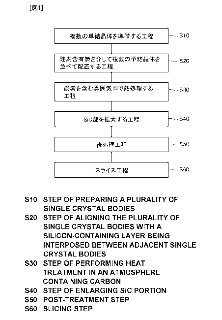
Fig. 1 is a flowchart showing a method for manufacturing a silicon carbide
substrate according to the present invention.
Fig. 2 is a schematic view for illustrating the method for manufacturing the
silicon carbide substrate shown in Fig. 1.
Fig. 3 is a schematic cross sectional view taken along a line III-III in Fig.
2.
Fig. 4 is a schematic view for illustrating the method for manufacturing the
silicon carbide substrate shown in Fig. 1.
-4-
CA 02775065 2012-03-22 111158:911363
Fig. 5 is a schematic view for illustrating the method for manufacturing the
silicon carbide substrate shown in Fig. 1.
Fig. 6 is a schematic view for illustrating the method for manufacturing the
silicon carbide substrate shown in Fig. 1.
Fig. 7 is a schematic view for illustrating the method for manufacturing the
silicon carbide substrate shown in Fig. 1.
Fig. 8 is a schematic view for illustrating the method for manufacturing the
silicon carbide substrate shown in Fig. 1.
Fig. 9 is a schematic planar view for illustrating another exemplary
arrangement
of the SiC single-crystal ingots in a step (S20) shown in Fig. 1.
Fig. 10 is a schematic planar view for illustrating still another exemplary
arrangement of the SiC single-crystal ingots in step (S20) shown in Fig. 1.
Fig. 11 is a schematic cross sectional view showing a variation of the process
in
step (S20) of Fig. 1.
Fig. 12 is a schematic cross sectional view showing another variation of the
process in step (S20) in Fig. 1.
Fig. 13 is a schematic cross sectional view showing still another variation of
the
process in step (S20) in Fig. 1.
Fig. 14 is a schematic cross sectional view showing yet another variation of
the
process in step (S20) in Fig. 1.
Fig. 15 is a schematic cross sectional view showing still another variation of
the
process in step (S20) in Fig. 1.
DESCRIPTION OF EMBODIMENTS
The following describes embodiments of the present invention with reference to
figures. It should be noted that in the below-mentioned figures, the same or
corresponding portions are given the same reference characters and are not
described
repeatedly.
Referring to Fig. 1 to Fig. 8, the following describes a method for
-5-
CA 02775065 2012-03-22 111158:911363
manufacturing a silicon carbide substrate according to the present invention.
As shown in Fig. 1, a step (S 10) is first performed by preparing a plurality
of
single-crystal bodies. Specifically, as shown in Fig. 2, a plurality of
silicon carbide
(SiC) single-crystal ingots 1 are prepared.
Next, a step (S20) is performed by arranging the plurality of single-crystal
bodies with a silicon-containing layer interposed therebetween. Specifically,
as shown
in Fig. 2, the plurality of SiC single-crystal ingots 1 are disposed such that
their
opposing end surfaces face each other with a Si layer 2 interposed
therebetween. Here,
Fig. 2 is a schematic perspective view showing a collected body configured by
arranging SiC single-crystal ingots 1 face to face with each other with Si
layer 2
interposed therebetween. As understood from Fig. 2 and Fig. 3, in this step
(S20), SiC
single-crystal ingots I are disposed such that their opposing end surfaces are
in contact
with Si layer 2. As Si layer 2, any type of layer can be used so far as it is
a layer
containing Si as its main component. For example, as Si layer 2, there can be
used a
sheet type member containing Si as its main component, or an object formed by
cutting
a Si substrate into a predetermined shape. Alternatively, as Si layer 2, there
may be
used a Si film formed on the end surfaces of SiC single-crystal ingots 1 by
means of,
for example, a CVD method or the like.
Further, SiC single-crystal ingots 1 arranged as shown in Fig. 2 preferably
have
almost the same crystal orientation. For example, in the collected body shown
in Fig.
2, each of SiC single-crystal ingots 1 may have a main surface (upper main
surface)
corresponding to a C plane, a Si plane, or any other crystal plane. Although
the
plurality of SiC single-crystal ingots 1 preferably have the same crystal
orientation as
described above, an error or the like introduced in a step of processing makes
it difficult
for them to have completely the same crystal orientation. Hence, the plurality
of SiC
single-crystal ingots 1 preferably have the following crystal orientations.
For example,
one SiC single-crystal ingot 1 having a predetermined crystal orientation is
regarded as
a reference. The other SiC single-crystal ingots 1 have corresponding crystal
-6-
CA 02775065 2012-03-22 111158:911363
orientations each having an angle of deviation (intersecting angle) of not
more than 5 ,
more preferably, not more than P.
Next, as shown in Fig. 1, a step (S30) is performed by performing heat
treatment in an atmosphere containing carbon. Specifically, the collected body
is
heated with a gas containing carbon being used as the atmosphere. For example,
the
heat treatment may be performed under conditions that: a hydrocarbon gas such
as
acetylene or propane is employed as the atmospheric gas; the atmosphere
pressure is set
at not less than 1 Pa and not more than an atmospheric pressure; the heating
temperature is set at not less than 1400 C and not more than 1900 C; and the
heating
retention time is set at not less than 10 minutes and not more than 6 hours.
As a result, carbon supplied from the atmosphere and silicon in Si layer 2
react
with each other to form SiC layers 3 at the upper end and lower end of Si
layer 2 (see
Fig. 3) as shown in Fig. 4. Here, Fig. 4 is a schematic cross sectional view
illustrating
a state of the collected body, which is the object subjected to the process in
the step
(S30) of Fig. 1. It should be noted that Fig. 4 corresponds to Fig. 3.
As shown in Fig. 4, adjacent SiC single-crystal ingots 1 are connected to each
other by SiC layers 3. SiC layers 3 may be formed through liquid phase epitaxy
of
SiC caused by partial melting of Si layer 2. For the formation of SiC layers
3, any
heat treatment conditions can be used.
Next, as shown in Fig. 1, a step (S40) is performed to expand the SiC
portions.
Specifically, by performing heat treatment, Si layer 2 (see Fig. 4) remaining
between
SiC layers 3 shown in Fig. 4 is converted into a SiC layer 4 as shown in Fig.
5.
In this step (S40), any method can be used to convert Si layer 2 into SiC
layer 4.
An exemplary method is to form a temperature gradient along a region between
SiC
single-crystal ingots 1 (region where SiC layer 4 is to be formed) (in the
upward/downward direction in Fig. 5 or in the thickness direction of the
collected body),
so as to grow a SiC layer from the SiC layer 3 sides to the Si layer 2 side
using a so-
called close-spaced sublimation method. An alternative method is to form a
-7-
CA 02775065 2012-03-22 111158:911363
temperature distribution along the upward/downward direction of the region in
Fig. 5 so
as to grow SiC from the SiC layer 3 sides by means of solution growth.
Further, in
this step (S40), the heat treatment may be performed under conditions that:
acetylene,
propane, or the like is used as a silicon carbide gas, i.e., the atmospheric
gas; the
atmosphere pressure is set at not less than 1 Pa and not more than atmospheric
pressure;
the heating temperature is set at not less than 1400 C and not more than 1900
C; and
the heating retention time is set at not less than 10 minutes and not more
than 6 hours.
Next, as shown in Fig. 1, a post-process step (S50) is performed.
Specifically,
from the region converted from Si layer 2 (see Fig. 2) into SiC layers 3, 4 as
described
above (hereinafter, also referred to as "connecting layer"), remaining silicon
(Si) is
removed, whereby the connecting layer contains SiC as its main component. In
this
step (S50), as shown in for example Fig. 6, the collected body constituted by
SiC
single-crystal ingots 1 and the connecting layer is placed on a susceptor 11
in a heat
treatment furnace 10, and is heated by a heater 12 through susceptor 11 with
the
atmosphere being under reduced pressure in heat treatment furnace 10. It
should be
noted that the pressure in the heat treatment furnace 10 can be adjusted by
discharging
the atmospheric gas therein using a vacuum pump 13 via a pipe 14 connected to
heat
treatment furnace 10. As a result, silicon is sublimated from the connecting
layer,
whereby the connecting layer can contain SiC as its main component.
It should be noted that in this post-process step (S50), as shown in Fig. 7,
the
collected body (also referred to as "connected ingot") constituted by SiC
single-crystal
ingots 1 and the connecting layer may be soaked in a hydrofluoric-nitric acid
solution
21 to remove silicon from the connecting layer. Here, Fig. 6 is a schematic
view for
illustrating an exemplary process in the post-process step (S50). Fig. 7 is a
schematic
view for illustrating another exemplary process in the post-process step
(S50).
Next, as shown in Fig. 1, a slicing step (S60) is performed. Specifically, the
collected body (connected ingot) obtained by connecting the plurality of SiC
single-
crystal ingots 1 using the connecting layer through steps (S10)-(S50) is cut
to obtain a
-8-
CA 02775065 2012-03-22 111158:911363
SiC-combined substrate 30 (see Fig. 8) having a main surface exhibiting an
appropriate
plane orientation. As a result, as shown in Fig. 8, SiC-combined substrate 30
thus
obtained has a first region 31 and a second region 32, both of which are
connected to
each other by a combining region 33. A device usable for this step (S60) is
any
conventionally known cutting device employing a wire saw or a blade (such as
an inner
peripheral cutting edge blade or an outer peripheral cutting edge blade). In
this way,
SiC-combined substrate 30 according to the present invention can be obtained.
Here, combining region 33 shown in Fig. 8 corresponds to SiC layers 3, 4
shown in Fig. 6. Further, first region 31 and second region 32 are parts of
SiC single-
crystal ingots I shown in Fig. 6. Further, first region 31 and second region
32 have
predetermined crystal orientations (for example, the <0001> direction) similar
to some
extent but not completely parallel. Such a difference in crystal orientation
can be
detected by means of, for example, diffraction orientation measurement on a
specific
plane by employing X-ray diffraction. For example, the difference in crystal
orientation can be checked using a method for detecting a displacement of peak
orientations by means of omnidirectional measurement performed using a pole
figure
method.
Further, first region 31 and second region 32 have crystallinity substantially
the
same in their thickness directions. Here, the crystallinity can be evaluated
from a half
width of diffraction angle, which is measured by means of XRD evaluation.
Further,
the phrase "crystallinity substantially the same in their thickness
directions" is
specifically intended to mean that variation of the above-described data in
the thickness
directions is equal to or smaller than a predetermined value (for example, the
variation
of the data is equal to or smaller than 10% relative to an average value).
Further,
based on the method of evaluating the crystallinity as described above, the
crystallinity
of combining region 33 is inferior to that of each of first region 31 and
second region
32.
It should be noted that in step (S20) shown in Fig. 1, as shown in Fig. 2, the
-9-
CA 02775065 2012-03-22 111158:911363
plurality of SiC single-crystal ingots 1 are arranged in columns and rows in
the form of
matrix but they can be arranged in another form. Referring to Fig. 9 and Fig.
10, the
following describes variations of the configuration of the collected body
having SiC
single-crystal ingots 1. Each of Fig. 9 and Fig. 10 is a schematic planar view
showing
the collected body formed by arranging the plurality of SiC single-crystal
ingots 1.
For example, as shown in Fig. 9, in the collected body including the plurality
of
SiC single-crystal ingots 1, the plurality of SiC single-crystal ingots 1 are
arranged in a
plurality of columns in step (S20) of Fig. 1 (although two columns are
provided in Fig.
9, three or more columns may be provided) in a predetermined direction
(upward/downward direction in Fig. 9) with Si layer 2 interposed therebetween.
Each
of SiC single-crystal ingots 1 is in contact with Si layer 2. The collected
body may be
configured such that locations of Si layer 2 in the predetermined direction
may differ
among the columns. In this case, Si layer 2 is configured to extend in three
directions
at a corner portion of each of SiC single-crystal ingots 1. On the other hand,
in the
arrangement of SiC single-crystal ingots 1 in the collected body shown in Fig.
2 and Fig.
3, Si layer 2 extends in four directions from the corner portion. Accordingly,
the
arrangement shown in Fig. 9 provides a smaller volume of Si layer 2 adjacent
to the
corner portion. This can restrain occurrence of such a problem that SiC layers
3, 4 are
not sufficiently formed from Si layer 2 due to a large volume of Si layer 2 at
the corner
portion in the structure in which SiC single-crystal ingots 1 are to be
connected to each
other by SiC layers 3, 4 (resulting from Si layer 2) (such a problem that the
structure
cannot be formed in which adjacent SiC single-crystal ingots 1 are
sufficiently
connected to each other by SiC layers 3, 4).
Further, an arrangement of the plurality of SiC single-crystal ingots 1
included
in the collected body as shown in Fig. 10 may be adopted in step (S20) of Fig.
1. In
Fig. 10, each of SiC single-crystal ingots I has a hexagonal planar shape. The
collected body is configured such that SiC single-crystal ingots 1 each having
this
hexagonal planar shape (i.e., external shape of hexagonal pillar) have end
surfaces
-10-
CA 02775065 2012-03-22 111158:911363
facing each other with Si layer 2 interposed therebetween. Also in such a
configuration, Si layer 2 extends in three directions at one corner portion of
each of SiC
single-crystal ingots 1, thereby attaining an effect similar to that in the
collected body
shown in Fig. 9.
Further, in the above-described method for manufacturing the silicon carbide
substrate, in step (S20), a cap member 5 may be provided to cover Si layer 2,
which is
to serve as the connecting layer, as shown in Fig. 11 or Fig. 12. It should be
noted that
each of Fig. 11 and Fig. 12 corresponds to Fig. 3. Referring to Fig. 11 and
Fig. 12, the
following describes variations of the configuration of the collected body
including SiC
single-crystal ingots 1 in step (S20) of Fig. 1.
As shown in Fig. 11 and Fig. 12, cap member 5 may be provided to cover Si
layer 2 in the collected body serving as a workpiece and having Si layer 2
interposed
between SiC single-crystal ingots 1. An exemplary, usable cap member 5 is a
substrate made of SiC. Cap member 5 basically has any planar shape so far as
it is
configured to cover the upper end surface of Si layer 2 along the planar shape
of Si
layer 2. For example, a plurality of substrates (for example, SiC substrates)
each
having a relatively small size may be arranged along the upper end of Si layer
2. This
can restrain Si from being sublimated and dissipated from SiC layers 3, 4 when
performing the heat treatment to convert Si layer 2 into SiC layers 3 and the
like (when
performing step (S30) or step (S40)), for example.
Further, as shown in Fig. 12, a cap Si layer 6 may be disposed under cap
member 5. Cap Si layer 6 thus disposed allows for improved adhesion between
cap
member 5 and each of SiC single-crystal ingots 1. Instead of cap Si layer 6, a
layer
(cap carbon layer) made of carbon (C) may be disposed.
Further, as shown in Fig. 13, instead of using cap member 5, the following
configuration may be employed. That is, a second layer 42 having a plurality
of SiC
single-crystal ingots 1 arranged is provided to cover the upper surface of a
first layer 41
having another set of plurality of SiC single-crystal ingots 1 arranged. First
layer 41
-11-
CA 02775065 2012-03-22 111158:911363
and second layer 42 are stacked on each other with an intermediate Si layer 7
interposed
therebetween. In each of first layer 41 and second layer 42, each of the end
surfaces of
adjacent SiC single-crystal ingots 1 is in contact with Si layer 2, which is
to become the
connecting layer.
On this occasion, it is preferable that the locations of Si layer 2 in contact
with
the end surfaces of SiC single-crystal ingots 1 in first layer 41 are
displaced from those
in second layer 42 when viewed in a planar view (they overlap with each other
only at a
part of the region thereof and most of them do not overlap at the rest of the
region). In
this way, for first layer 41, second layer 42 can be used as a member that
provides an
effect similar to that provided by the above-described cap member. Further,
with the
structure obtained by stacking the two or three layers of SiC single-crystal
ingots 1, a
larger SiC single-crystal collected body (combined ingot) can be obtained.
The following describes another variation in step (S20) of Fig. 1, with
reference
to Fig. 14 and Fig. 15. Each of Fig. 14 and Fig. 15 corresponds to Fig. 3.
As shown in Fig. 14, in step (S20) of Fig. 1, SiC single-crystal ingots 1 are
arranged on a base material 45 with a space 46 therebetween. Further, a cap Si
layer 6
is disposed to cover space 46. On cap Si layer 6, a cap member 5 made of SiC
is
disposed. In this state, the entire collected body shown in Fig. 14 is heated
to a
predetermined temperature, thereby melting cap Si layer 6. This temperature is
a
temperature at which cap Si layer 6 melts (temperature higher than the melting
point of
silicon) and is lower than the temperature at which silicon carbide sublimes.
In this
heat treatment, for example, the heating temperature can be set at not less
than 1400 C
and not more than 1900 C, more preferably, not less than 1500 C and not more
than
1800 C. Further, the Si melt formed as a result of melting of cap Si layer 6
flows into
space 46 shown in Fig. 14. Thereafter, the temperature is decreased to fall
below the
melting point of silicon, thereby solidifying the Si melt having flown into
space 46.
As a result, as shown in Fig. 15, an inflow Si layer 52 is provided as the
solid in
the space between SiC single-crystal ingots 1. Further, cap member 5 described
above
-12-
CA 02775065 2012-03-22 111158:911363
covers the upper end surface of inflow Si layer 52. In this way, there can be
obtained
the collected body in which SiC single-crystal ingots 1 are combined to each
other as
shown in Fig. 2 and Fig. 3. Such an inflow Si layer 52 can be also converted
into SiC
layers by performing step (S30) to step (S50) shown in Fig. 1. As a result,
the single-
crystal ingot collected body (combined ingot) can be obtained in which SiC
single-
crystal ingots 1 are connected to each other by the connecting layer
(combining layer)
constituted by the SiC layers. Then, step (S60) of Fig. 1 is performed,
thereby
obtaining the SiC-combined substrate. It should be noted that the respective
configurations of the above-described embodiments can be combined
appropriately.
The following describes characteristic configurations of the present
invention,
although some of them have been already described above.
The method for manufacturing the silicon carbide substrate according to the
present invention is a method for manufacturing a SiC-combined substrate. The
method includes: the step (S 10) of preparing a plurality of single-crystal
bodies each
made of silicon carbide (SiC); the step (step (S20) in Fig. 1) of forming a
collected
body; the step (step (S30) in Fig. 1) of connecting the single-crystal bodies
to each
other; and the step (step (S60) in Fig. 1) of slicing the collected body. In
the step
(S20) of forming the collected body, the collected body including the single-
crystal
bodies is formed by arranging the plurality of single-crystal bodies (SiC
single-crystal
ingots 1) with a silicon (Si) containing connecting layer (Si layer 2,
intermediate Si
layer 7, or inflow Si layer 52) interposed therebetween. In the step (S30) of
connecting the SiC single-crystal ingots 1 to each other, SiC single-crystal
ingots 1 are
connected to each other by the connecting layer (Si layer 2, intermediate Si
layer 7, or
inflow Si layer 52) via at least a portion of the connecting layer, the at
least portion
being formed into silicon carbide by heating the collected body. In the
slicing step
(S60) of slicing the collected body, the collected body in which SiC single-
crystal
ingots 1 are connected to each other is sliced.
Thus, the plurality of SiC single-crystal ingots 1 are connected to each other
by
- 13 -
CA 02775065 2012-03-22 111158:911363
SiC layers 3, 4, each of which serves as the connecting layer formed into
silicon carbide,
so as to form a large ingot (combined ingot) of silicon carbide. Then, this
ingot is
sliced. In this way, there can be efficiently obtained a plurality of silicon
carbide
substrates (SiC-combined substrates 30) each having a size larger than that of
a silicon
carbide substrate obtained by slicing one single-crystal body. When such a SiC-
combined substrate 30 having a large size is employed to manufacture
semiconductor
devices, a greater number of semiconductor devices (chips) can be formed from
one
SiC-combined substrate 30, as compared with the number in the conventional
one. As
a result, the manufacturing cost of the semiconductor devices can be reduced.
Further, the large ingot formed as described above is sliced to obtain silicon
carbide substrates (SiC-combined substrates 30) of the present invention.
Hence, a
plurality of SiC-combined substrates can be manufactured at one time as
compared with
a case of forming SiC-combined substrates (silicon carbide substrate) one by
one by
connecting single-crystal bodies having a relatively thin thickness to each
other.
Accordingly, the manufacturing cost of SiC-combined substrates 30 can be
reduced as
compared with the case of forming silicon carbide substrates (SiC-combined
substrates)
one by one by connecting single-crystal bodies each having a thin thickness.
The method for manufacturing the silicon carbide substrate may further include
the step (step (S50) in Fig. 1) of removing silicon from the connecting layer
after the
step of connecting (step (S30) in Fig. 1) and before the step of slicing (step
(S60) in Fig.
1).
In this case, no silicon (Si) remains in SiC layers 3, 4 each serving as the
connecting layer. This restrains occurrence of a problem resulting from
silicon
remaining in SiC layers 3, 4 (combining region 33 in SiC-combined substrate
30). For
example, if silicon remains in combining region 33 serving as the connecting
layer of
the silicon carbide substrate (SiC-combined substrate 30), silicon may be
released to
outside from combining region 33 when a temperature in heat treatment for SiC-
combined substrate 30 or the like is around the melting point of silicon. When
silicon
-14-
CA 02775065 2012-03-22 111158:911363
is thus released from combining region 33 to outside, density of combining
region 33 is
decreased to highly likely result in decreased hardness in combining region
33. The
decreased hardness in combining region 33 may result in damage of SiC-combined
substrate 30 or may result in the released silicon providing an adverse effect
over the
process on SiC-combined substrate 30. However, by performing the above-
described
step (S50), occurrence of the above-described problems can be restrained.
In the step of connecting (step (S30) in Fig. 1) in the method for
manufacturing
the silicon carbide substrate, a liquid phase epitaxy method (LPE method) may
be
employed to form the at least portion of the connecting layer (Si layer 2,
intermediate Si
layer 7, or inflow Si layer 52) into silicon carbide. In this case, the
portion of Si layer
2 can be securely formed into silicon carbide.
In the step of connecting (step (S30) in Fig. 1) in the method for
manufacturing
the silicon carbide substrate, the portion of the connecting layer (Si layer 2
and
intermediate Si layer 7) is formed into silicon carbide. Further, the method
for
manufacturing the silicon carbide substrate may further include the step (step
(S40) in
Fig. 1) of growing silicon carbide from the portion (SiC layers 3) formed into
silicon
carbide in the connecting layer to a portion (for example, Si layer 2 of Fig.
4) not
formed into silicon carbide in the connecting layer by heating, after step
(S30) of Fig. 1,
i.e., after the step of connecting, the collected body to form a temperature
gradient in
the direction in which the connecting layer extends (for example, in the
thickness
direction thereof, which is the direction in which Si layer 2 extends).
Further, in the
step of connecting (step (S30) in Fig. 1), the collected body may be heated in
an
atmosphere containing carbon.
In this case, a ratio of silicon carbide in the connecting layer formed into
silicon
carbide can be increased. Accordingly, SiC single-crystal ingots 1 can be
connected to
each other with improved strength provided by the connecting layer thus formed
into
silicon carbide (SiC layers 3, 4 of Fig. 6, also referred to as connection
layer).
In the step (step (S20) in Fig. 1) of forming the collected body in the method
for
-15-
CA 02775065 2012-03-22 111158:911363
manufacturing the silicon carbide substrate, a sheet type member containing
silicon as
its main component may be used as the connecting layer (Si layer 2 or
intermediate Si
layer 7). In this case, the sheet type member is disposed between SiC single-
crystal
ingots 1, thereby readily constituting the collected body.
In the method for manufacturing the silicon carbide substrate, the step (step
(S20) in Fig. 1) of forming the collected body may include: the step of
arranging the
plurality of SiC single-crystal ingots 1 with a space therebetween as shown in
Fig. 14;
the step of disposing a connecting member (cap Si layer 6 of Fig. 14) to cover
the space,
the connecting member containing silicon as its main component; and the step
of
forming the connecting layer (inflow Si layer 52) by heating and melting the
connecting
member (cap Si layer 6) and letting the melted connecting member flow into the
space.
In this case, the melted connecting member flows into the space, thereby
entirely filling the space with melted cap Si layer 6. The space thus filled
with inflow
Si layer 52 allows the connecting member (i.e., inflow Si layer 52) to
securely make
contact with the end surfaces (surfaces at the space) of SiC single-crystal
ingots 1.
Accordingly, a portion obtained by forming inflow Si layer 52 into silicon
carbide can
make contact with SiC single-crystal ingots 1 more securely.
In the step (step (S20) in Fig. 1) of forming the collected body in the method
for
manufacturing the silicon carbide substrate, a chemical vapor deposition
method (CVD
method) may be employed to form the connecting layer (Si layer 2 or
intermediate Si
layer 7). In this case, unlike the step of preparing the sheet type connecting
layers and
disposing them between SiC single-crystal ingots I individually, Si layer 2
can be
formed all at once using the CVD method in the predetermined space which is
interposed between the plurality of SiC single-crystal ingots 1. Accordingly,
the step
(step (S20) in Fig. 1) of forming the collected body can be simplified, which
results in
reduced manufacturing cost of SiC-combined substrate 30.
In the step (step (S30) in Fig. 1) of connecting in the method for
manufacturing
the silicon carbide substrate, the collected body may be heated with a cover
member
-16-
CA 02775065 2012-03-22 111158:911363
(cap member 5) provided to cover the end surface of the connecting layer (Si
layer 2,
intermediate Si layer 7, or inflow Si layer 52). In this case, when the
portion of the
connecting layer (Si layer 2) is formed into silicon carbide in step (S30) in
Fig. 1,
silicon is restrained from being released from Si layer 2, and Si layer 2,
i.e., the
connecting layer is restrained from being temporarily melted and leaked from
the region
in which Si layer 2 is disposed (space between SiC single-crystal ingots 1).
In the method for manufacturing the silicon carbide substrate, the cover
member
(cap member 5) may contain one of silicon carbide (SiC) and carbon (C) as its
main
component. In this case, cap member 5 is constituted by a material having a
sufficiently high melting point. Hence, cap member 5 can be prevented from
being
damaged by the heat treatment performed in step (S30).
In the step (step (S30) in Fig. 1) of connecting in the method for
manufacturing
the silicon carbide substrate, an intermediate layer (cap Si layer 6) may be
disposed
between cap member 5 and the collected body. In this case, unlike the material
of cap
member 5, a material excellent in adhesion with the collected body (SiC single-
crystal
ingots 1 and Si layer 2 serving as the connecting layer) can be selected as
the material
of the intermediate layer. Accordingly, the end surface of Si layer 2 serving
as the
connecting layer can be securely covered with cap member 5 and cap Si layer 6.
In the method for manufacturing the silicon carbide substrate, the
intermediate
layer (cap Si layer 6) may contain one of silicon (Si) and carbon (C) as its
main
component. Particularly, in the case where silicon is used for the
intermediate layer,
adhesion between the intermediate layer and the collected body can be improved
more.
A SiC-combined substrate 30, which is a silicon carbide substrate according to
the present invention, includes: a plurality of single-crystal regions (first
region 31 and
second region 32 in Fig. 8) each made of silicon carbide; and a connecting
layer
(combining region 33). Combining region 33 is made of silicon carbide (SiC),
is
located between the plurality of single-crystal regions (first region 31 and
second region
32), and connects the single-crystal regions (first region 31 and second
region 32) to
-17-
CA 02775065 2012-03-22 111158:911363
each other. The single-crystal regions (first region 31 and second region 32)
are
formed to extend from the first main surface of SiC-combined substrate 30
(upper main
surface in Fig. 8) to the second main surface thereof opposite to the first
main surface
(the underlying backside surface of SiC-combined substrate 30). Crystallinity
in the
single-crystal regions (first region 31 and second region 32) are
substantially the same
in the direction of thickness from the first main surface to the second main
surface.
The plurality of single-crystal regions (first region 31 and second region 32)
are
different from each other in terms of crystal orientation in the first main
surface.
Combining region 33 has crystallinity inferior to that of each of the single-
crystal
regions (first region 31 and second region 32).
With the configuration described above, the plurality of single-crystal
regions
(first region 31 and second region 32) are connected by combining region 33.
Accordingly, there can be realized a silicon carbide substrate (SiC-combined
substrate
30) having a main surface having a larger area than that of a silicon carbide
substrate
constituted by one single-crystal region. Accordingly, a larger number of
semiconductor devices can be obtained from one silicon carbide substrate
during
formation of semiconductor devices. This leads to reduced manufacturing cost
of the
semiconductor devices.
Further, the single-crystal regions (first region 31 and second region 32)
have
substantially the same crystallinity in the direction of thickness from the
first main
surface to the second main surface. Hence, when forming a vertical type
device, no
problem takes place due to locally inferior crystallinity in the thickness
direction of
SiC-combined substrate 30.
The embodiments disclosed herein are illustrative and non-restrictive in any
respect. The scope of the present invention is defined by the terms of the
claims,
rather than the embodiments described above, and is intended to include any
modifications within the scope and meaning equivalent to the terms of the
claims.
INDUSTRIAL APPLICABILITY
-18-
CA 02775065 2012-03-22 111158:911363
The present invention is particularly advantageously applied to a substrate
having a structure obtained by combining a plurality of single-crystal bodies
each made
of silicon carbide.
REFERENCE SIGNS LIST
1: SiC single-crystal ingot; 2: Si layer; 3, 4: SiC layer; 5: cap member; 6:
cap Si
layer; 7: intermediate Si layer; 10: heat treatment furnace; 11: susceptor;
12: heater; 13:
vacuum pump; 14: pipe; 21: hydrofluoric-nitric acid solution; 30: SiC-combined
substrate; 31: first region; 32: second region; 33: combining region; 41:
first layer; 42:
second layer; 45: base material; 46: space; 52: inflow Si layer.
_19-