Note: Descriptions are shown in the official language in which they were submitted.
CA 02776897 2012-04-05
WO 2011/042348
PCT/EP2010/064508
RECONFIGURABLE ACTIVE COMPUTATIONAL BEAMFORMING ANTENNA
The field of the invention relates to reconfigurable
active computational beamforming antennas, notably for
the antennas intended for onboard applications, for
wideband requirements.
The active digital beamforming (DBF) antennas generally
consist of digital beamformers in order to meet the
mission flexibility needs when a large number of beams
(also commonly called "spots") have to be formed. The
mission flexibility relates in particular to the
coverage area, the bandwidth and the center frequency
for each beam, the power for each beam, the number of
beams, and the selection of the radiating elements
used. These antennas are particularly well suited to
onboard applications for satellite, aircraft or ship
type craft for example, requiring dynamic antenna
pointing control because of the specific movement of
the platform. Using digital processing, these DBF
antennas make it possible to perform (to a certain
extent) the repointing operation, but also to calibrate
and to compensate the physical imperfections of the
antenna system, throughout the mission. The digital
processing operations can be performed on baseband, or
intermediate frequency (IF) digitized signals, or even
directly on radiofrequency (RF) carriers. The advantage
of the DBF antennas for telecommunication satellite
applications can be illustrated as an example.
Generally, the mission of the latter is to cover
extensive geographic areas by means of a multitude of
narrow and contiguous beams, producing a cellular
coverage. For certain beams, a higher bandwidth can be
assigned, making it possible, for example, to offer
high definition video services. The coverage area can
also be modified during the lifetime of the satellite,
as can the frequency plan for incorporating new
linguistic spots for example. The flexibility of the
DBF antennas makes it possible to meet the trend of the
CA 02776897 2012-04-05
WO 2011/042348 - 2 -
PCT/EP2010/064508
services while keeping the same hardware architecture.
In another example, notably for military
telecommunication satellite applications, there may be
intentional scramblers to be confronted. A DBF antenna
makes it possible on the one hand to identify the
direction of the scramblers, and on the other hand to
mask (by forcing a zero gain) these directions, in
order to improve the signal-to-noise ratio of the
considered signals. For the same military applications,
the coverage areas are naturally variable to address
different theaters of operations during the lifetime of
the satellite.
Because of the increasing need in terms of processed
bandwidth, it is becoming necessary to increase both
the bandwidth for each beam (from a few tens to a few
hundreds of MHz) and the number of beams (typically
from a few tens to more than a hundred or so beams).
The use of DBF antennas requires a large number of
radiating elements, typically of the order of a few
tens to a few hundreds depending on the antenna type
(for example DRA: "Direct Radiating Array", AFR: "Array
Fed Reflector"). The digital processing for beamforming
performs a linear combination on the input signals, or
respectively the signals obtained from the radiating
elements in the reception case, and the beams to be
transmitted in the transmission case. The transmission
and reception cases are similar and require the same
processing operations. The computation functions for
beamforming involve a complex weighting coefficient
assignment operation, a complex multiplication
operation for each beam, for each radiating element and
for each data sample, as well as a complex addition to
combine the duly computed partial terms. More
specifically, as illustrated by figure 3, the
beamforming function is performed by means of combiners
assigning the weighting coefficients 11011, 11021,
11031 and performing the complex multiplication 1101,
CA 02776897 2012-04-05
WO 2011/042348 - 3 -
POT/131)2010/064508
1102, 1103 and complex addition 1201, 1202, 1203
operations on the partial terms. These combiners are
assembled to perform the different linear combinations
corresponding to the beamforming. As illustrated by
figures 1 (reception case) and 2 (transmission case), a
DBF antenna comprises a set of boards and electronic
equipment items 701, 702; 711, 712 incorporating the
digital components performing these processing
operations. The design of such antennas is
problematical for onboard applications, because of the
logical complexity and the dissipation of power.
The processed bandwidth associated with the quantity of
beams to be formed and with the multitude of radiating
elements mobilized induces a very dense connectivity
between the computation units (integrated circuits) and
high-throughput needs on the interfaces of the digital
components. These components are usually ASICs
(Application-Specific Integrated Circuits) or FPGAs
(Field Programmable Gate Arrays). The input and output
interfaces of these components are quickly saturated
whereas the capacity in terms of logic gates for
implanting the DBF processing operations is under
exploited. The result of this is increased hardware
complexity, which is not optimal with a large number of
components underused. The result of this is an increase
in the weight, the bulk, the dissipation and the cost
of the systems, raising problems of feasibility given
the constraints of the onboard applications. Antennas
of DBF type are known, described in the patent
application FR2864710 Al filed on 12/24/2003. This
document describes an array architecture for this type
of antenna.
To overcome these problems of hardware complexity and
dissipation, the consideration of two solutions is
generally envisaged. The first solution consists in
using the most advanced microelectronic technologies,
CA 02776897 2012-04-05
WO 2011/042348 - 4 -
PCT/EP2010/064508
to benefit from the gains in integration density, in
processing speed, in dissipation, and in throughput of
the interfaces. However, the cost associated with these
technologies regularly increases and may prove
prohibitive. Also, the renewal cycles of the
microelectronic technologies tend to slow down for
etching finenesses less than 90 nm. This solution is
proving increasingly inadequate to meet the trend of
the requirements regarding computational beamforming.
Architecture studies performed to assess the
feasibility of future wideband missions
(telecommunication satellites) show that the gap is
widening between, on the one hand, the trend of the
wideband DBF requirements, and, on the other hand, what
would be made possible by the technological trend in
the medium term, given constant weight and dissipation
constraints.
A second solution that can be envisaged lies in the
known techniques of optimizing the implantation of the
computations when the operands are fixed. In the case
of DBF function, this imposes complex weighting
coefficients that are fixed in relation to the
definition of the circuits. The flexibility inherent to
the reprograming of all the weighting coefficients can
then be obtained only with reprograming at the circuit
level. This solution therefore imposes the use of
reconfigurable FPGA components. However, these
components have integration capacities much lower than
the ASIC components. The number of reconfigurable FPGA
components needed for the DBF function would then be
too high, compromising the feasibility with respect to
the hardware complexity and dissipation.
The patent document WO 2008/075099 "Beamforming system
and method", proposing a solution making it possible to
reduce the complexity of implantation of the DBF
function, in transmission and/or reception, in the case
CA 02776897 2016-12-29
- 5 -
of active AFR-type antennas, is known. This type of
antenna forms a beam with a subset of the feeds, and
the proposed solution is to implant a selector
("switch") of feeds upstream of the DBF, rather than
implant a linear combination on all the feeds and force
the zero weighting for the unused feeds. Nevertheless,
this solution only addresses the case of AFR antennas
and does not resolve the problems of congestion of the
interfaces of the integrated circuits, in the wideband
case and for a large number of beams, resulting in high
complexities and dissipation.
The present invention has been made in view of the
abovementioned problems associated with multibeam active
antennas.
The present invention relates to a system
for transmitting and/or receiving of multibeam
computational beamforming antenna type comprises an
array of radiating elements capable of transmitting
and/or receiving RF (radiofrequency) signals. The
computational beamforming function applies equally well
in transmission and in reception. In reception, a beam
is formed by complex linear combination of the
digitized data, in baseband, or in IF or directly in
RF, obtained, possibly after frequency transposition
and filtering, from the RF signals received by a group
of radiating elements. In transmission, a beam is
formed by generating the excitation signals for the
radiating elements by complex linear combination of the
digital signals, in baseband or in IF or directly in
RF, of the beams to be generated, before digital/analog
conversion and possible frequency transposition.
More specifically, the invention relates to an
apparatus for processing data from at least one digital
signal for a system for transmitting and/or receiving
RF signals of active antenna type comprising a
plurality of radiating elements and capable of forming
CA 02776897 2012-04-05
WO 2011/042348 - 6 -
PCT/EP2010/064508
at least one beam by computation using a plurality of
combiners. For this, the data processing apparatus
comprises at least two combiner arrays, at least one
vector converter and one inverse converter.
The vector converter comprises an input channel and at
least two output channels, and is capable of converting
an integer digital datum from a digital signal present
on the input channel into a datum in vector
representation by at least two components in residue
arithmetic on the output channels, one output channel
being dedicated to each component.
The inverse converter comprises at least two input
channels and one output channel, and is capable of
converting the datum in vector representation defined
by at least two components in residue arithmetic
present on the input channels into an integer digital
datum on the output channel, one input channel being
dedicated to each component.
The vector converter and the inverse converter are
arranged on either side of the combiner arrays and the
combiner arrays are arranged so as to process in
parallel said components in residue arithmetic to form
the beam in reception mode or the excitation signal of
a radiating element of the antenna in transmission
mode, one combiner array performing the processing
operations associated with a specific component in
residue arithmetic.
According to any one of the vector representation
modes, a first component in residue arithmetic is
represented in an integer format on a first dynamic and
a second component in residue arithmetic is represented
in an integer format on a second dynamic. The integer
digital datum present on the input of a vector
converter is represented in an integer format on a
CA 02776897 2012-04-05
WO 2011/042348 - 7 -
PCT/EP2010/064508
dynamic equal to m, and the dynamic of a component in
residue arithmetic represented in an integer format is
strictly less than m.
In residue arithmetic, the integer numbers are
represented by vectors, and the arithmetic processing
operations are vectorized: performed independently by
components, or computation plane. Instead of
conventionally performing the operations on integers on
n bits (implicitly modulo 2"), the computations are
performed in parallel on r integer components, modulo
respectively ml, m2, .. mr. The choice of modulus base
{ml, m2, mr} has to
satisfy two conditions: on the
one hand, the moduli mi. have to be coprimes, and, on the
other hand, the product of all the moduli has to be
greater than 2" to represent an integer dynamic on n
bits. Each computation plane (i) performs the
processing operations modulo one integer m,, with a
specific dynamic mi well below 2". This system of
vectorized representation of the numbers in residue
arithmetic is also commonly called "residue number
system" (RNS).
Advantageously, a combiner array processes the first
component independently of the second component.
Advantageously, the apparatus comprises, for the
forming of a beam, a number of independent combiner
arrays equal to the number of components in residue
arithmetic obtained from a vector converter.
The DBF function comprises as many independent combiner
arrays for each beam as the dimension of the base (at
least two) chosen to perform the processing operations
in residue arithmetic. Thus, on a functional plane, an
antenna in reception generating N beams, from i
radiating elements, in residue arithmetic with r
components, will implant N*r arrays of i combiners,
CA 02776897 2012-04-05
WO 2011/042348 - 8 -
PCT/EP2010/064508
associated with i vector converters (1 :r) and N
inverse converters (r :1), each function
being
dimensioned to process the throughput corresponding to
the bandwidth required for each beam. However, those
skilled in the art can adapt the use of the physical
resources to the functional need to optimize the
complexity.
According to a first variant of the invention, the
apparatus comprises at least one type of implementation
means integrating the vector converters, the inverse
converters and the combiner arrays capable of
processing the first and the second component. The
expression "type of implementation means" should be
understood to mean any type of electronic components
such as FPGA or ASIC circuits, or a set of electronic
components forming an electronic circuit board or a
sub-equipment item comprising a number of boards.
According to a second variant of the invention, more
modular and suited to the wideband DBF requirement, the
apparatus comprises at least three types of
implementation means, a first implementation means
being dedicated to the integration of combiner arrays,
a second implementation means being dedicated to the
integration of the vector converters and a third
implementation means being dedicated to the integration
of the inverse converters. This implantation makes it
possible to optimize the complexity and dissipation,
the dimensionings of these three functions being
specific. The interfaces (inputs and/or outputs) of the
different implementation means (boards/circuits) are
then, in residue arithmetic, identifiable by the coding
of the data and the different dynamics of the
components in residue arithmetic.
According to a variant, the DBF function forms all the
beams on one and the same bandwidth or in another, more
CA 02776897 2012-04-05
WO 2011/042348 - 9 -
PCT/EP2010/064508
effective variant, the apparatus also comprises digital
signal processing means, notably means for multiplexing
narrowband digital signals and/or means for demulti-
plexing a wideband digital signal, capable of being
arranged upstream or downstream of the combiner arrays
in the data processing chain formed by the combiner
arrays and said processing means.
The vector converters can be arranged upstream of these
digital signal processing means and the inverse
converters downstream of the digital signal processing
means, the digital signal processing means processing
the data also in residue arithmetic. However, the DBF
function may be the only one to process the data in
vectorized representation, the vector converters being
arranged directly upstream of the DBF function and the
inverse converters directly downstream of the DBF
function.
Thus, the DBF function can form the beams on different
bandwidths, respectively downstream of a frequency
demultiplexer or filter bank in the reception case, and
upstream of a frequency multiplexer in the transmission
case. Advantageously, the hardware resources and the
power dissipation are mobilized only to process the
considered signal (frequency channel associated with a
direction). Advantageously, the individual combiner
arrays are dimensioned to process the throughput
corresponding to the individual frequency band of the
demultiplexer or of the frequency multiplexer, to
optimize the complexity and the dissipation. The
combiner arrays are then assembled on four dimensions:
by RNS components, by beams, by radiating elements, and
by individual frequency band.
According to a variant of the apparatus for an antenna
comprising a plurality of radiating elements and
capable of forming at least two beams from n radiating
CA 02776897 2012-04-05
WO 2011/042348 - 10 -
PCT/EP2010/064508
elements, at least one radiating element being common
for the forming of said beams, the combiners processing
the same component of the digital signal data obtained
from said radiating element common to said beams are
implemented in one and the same electronic component.
In the case of the DBF antennas comprising a lens or a
reflector, for example an AFR-type antenna, all the
radiating elements do not necessarily contribute to
forming each beam, unlike in the DR A case. Any
radiating element generally contributes to forming a
set of adjacent beams in the reception case and,
symmetrically, any beam contributes to the excitation
of a set of adjacent radiating elements in the
transmission case. Advantageously for this type of
antenna, by pooling the interfaces, that is to say by
combining the processing operations sharing the same
data as input, the implantation of the DBF in residue
arithmetic makes it possible, because of the reduced
complexity (in terms of surface area and of throughput
at the interfaces) for each computation plane, to
integrate a greater number of processing operations for
each ASIC/FPGA circuit, resulting in a reduced
dissipation and overall complexity.
According to a variant, a digital
apparatus/board/combiner array type circuit implants
combiners for a subset of the computation planes.
Advantageously, this option makes it possible to relax
the constraint on throughput at the interfaces, at the
apparatus, electronic circuit board and ASIC/FPGA
components level.
According to a variant, an apparatus/board/digital
circuit of combiner array type implants combiners on
all the computation planes. Advantageously, all the
combiner arrays of the DBF can be implanted with one
and the same type of apparatus, even with one and the
CA 02776897 2012-04-05
WO 2011/042348 - 11 -
PCT/EP2010/064508
same type of ASIC/FPGA, to optimize the development and
production costs.
Despite the additional complexity induced by the vector
and inverse converters, this vectorized representation
is particularly advantageous for the wideband DBF
function, involving a large number of multipliers and
operating at high throughput. In practice, the
parallelism makes it possible to speed up the
arithmetic processing operations on a number of
computation planes of lesser complexity, with a reduced
dynamic for each computation plane, which also reduces
the throughput at the interface of the processing
functions for each computation plane. The implantation
granularity is greatly enhanced, as much on the plane
of interfaces (functional throughput reduced together
with the dynamic) as on the plane of the logical
complexity of the individual processing operations
(operations on reduced dynamics), which makes it
possible to better exploit the integration capacities
of the ASIC and/or FPGA components, resulting in a
lesser complexity of implantation of the DBF function.
Also, the dissipation and the processing speed of the
DBF function are also enhanced by virtue of the reduced
dynamic of the individual operators (adders,
multipliers).
According to a variant, the vector converters, the
inverse converters and the combiners are designed by
means of FPGA type components. In practice, the reduced
granularity of the individual computation functions
makes it possible to use FPGAs, which offer a lesser
integration capacity than the ASICs.
The implementation of DBF functions according to the
invention offers a number of advantages compared to the
conventional techniques in the case of requirements
CA 02776897 2016-12-29
- 12 -
that are demanding in terms of beams, radiating elements
and wideband.
A first possible advantage in the subdividing of the
processing operations by independent computation planes
is the significant reduction of the throughput at the
interfaces for each individual combiner function, which
generally constitutes a factor limiting the
effectiveness of the hardware architectures.
A second possible advantage, extending the first, is the
reduction in the granularity of implantation of the
individual combiner function, in terms of surface area,
and in terms of dissipation, as well as in terms of
interface, allowing for a better use of the hardware
resources, for a lesser complexity and overall
dissipation.
A third possible advantage, linked to the second, is the
introduction of a new modularity dimension, by
computation plane, complementing the dimensions by
beam, by radiating element, and by individual frequency
band, for a greater design flexibility and modularity.
For example, an ASIC performing DBF processing
operations on a particular computation plane (modulo
13, etc.) can be reused if the overall computation
dynamic had to change for another DBF antenna.
A fourth possible advantage, also resulting from the
second, is the possibility of using less powerful
microelectronic technologies, FPGAs or ASICs of lesser
integration capacity or that are less fast, to reduce
the costs.
A fifth possible advantage, inherent to the reduced
dynamic by computation plane and to the simplification
of the arithmetic operators, is the reduction in
dissipation associated with an enhancement of the
critical operating frequency.
CA 02776897 2016-12-29
- 13 -
A sixth possible advantage, linked to the first, makes
it possible to integrate more DBF processing operations
for each integrated circuit, by pooling the interfaces
for the processing operations concerning one and the same
set of inputs, in the case of the DBF AFR antennas or
antennas comprising a lens.
According to an aspect of the present invention there is
provided a system for transmitting and/or receiving RF
signals, called multibeam active antenna, wherein it
comprises an apparatus as described herein.
According to another aspect of the present invention
there is provided a telecommunication satellite,
comprising a system as described herein.
The invention therefore may make it possible to achieve
the aims sought for the onboard applications.
The invention will be better understood and other
advantages will become apparent from reading the
following description given as a nonlimiting example
and by virtue of the appended figures in which:
Figure 1 represents the block diagram of the data
processing chain of a DBF antenna in reception mode.
Figure 2 represents the block diagram of the data
processing chain of a DBF antenna in transmission mode.
Figure 3 represents the block diagram of the digital
channel forming processing, common to both transmission
and reception modes.
Figure 4 represents a DBF antenna of AFR type, and the
illumination of the feeds by the focal spots.
Figure 5 represents the block diagram of an individual
combiner, computing and accumulating a partial term of
the DBF computation.
CA 02776897 2016-12-29
- 13a -
Figure 6 represents an example of matrix assembly of
the combiners to form a set of channels from one and
the same set of inputs.
Figure 7 represents a block diagram of digital
processing in RNS.
CA 02776897 2012-04-05
WO 2011/042348 - 14 -
PCT/EP2010/064508
Figure 8 represents the block diagram of an
implementation of DBF processing in RNS.
Figure 9 represents the pooling of the interfaces
(radiating elements in the reception case) to
effectively form adjacent beams.
The invention applies to the active DBF antennas of DRA
type and the antennas comprising a reflector (FAFR,
standing for "Focal Array Fed Reflector" and AFR,
standing for "Array Fed Reflector", for example). It
applies to any active DBF antenna and preferably to the
antennas comprising an array of radiating elements
consisting of a large number of feeds, that is to say,
by way of indication, up to more than a hundred or so,
and intended to form a multitude of wideband beams,
that is to say, by way of indication, up to a hundred
or so beams over a frequency band of approximately 100
to 500 MHz. However, the latter indications in no way
limit the scope of the invention. The invention applies
advantageously to more complex antennas that may
comprise a greater number of radiating elements and
that can transmit and/or receive a greater number of
beams over wider frequency bands. The embodiment
described hereinbelow relates in particular to an
onboard antenna for satellites.
As represented in figure 1, the antenna in reception
mode according to the invention comprises radiating
elements 10, 11, 12, connected to analog input chains
performing operations for filtering 210, amplification
310, possibly frequency transposition 410 into
intermediate frequency or into baseband, analog/digital
converters 510, possibly frequency demultiplexing
functions 610, and computational beamforming functions
701, 702. The digital signal at the output of the ADC
is wideband. The channeling by frequency demultiplexing
610 can be performed before or after the DBF. In an
CA 02776897 2012-04-05
WO 2011/042348 - 15 -
PCT/EP2010/064508
advantageous embodiment, the channeling is performed
before the DBF, which then processes a multitude of
narrowband signals 611, 612, 613. The outputs 611, 614
of each frequency demultiplexer 610 are connected to
the inputs of a set 701, 702 of beamformers, which
generate the digital signals 801, 802 resulting from
the spatial filtering producing the antenna gain in the
desired directions.
Symmetrically, as represented in figure 2, the antenna
in transmission mode according to the invention
comprises radiating elements 60, 61, connected to
analog output chains performing operations for
filtering 260, amplification 360, frequency
transposition 460, digital/analog converters 560,
possibly frequency multiplexing functions 660, and
computational beamforming functions 711, 712. The
digital signal at the input of the DAC is wideband. The
frequency multiplexing 660 can be performed before or
after the DBF. In an advantageous embodiment, the
frequency multiplexing is performed after the DBF,
which then processes a multitude of narrowband signals
852, 857, 862, 867. The inputs of each frequency
multiplexer 660 are connected to the outputs 652, 651
of a set 711, 712 of beamformers which construct the
excitation signal for a radiating element, in an
individual frequency band.
The DBF digital processing, also called channel
forming, is identical in transmission and in reception,
and corresponds to a complex linear combination on the
inputs. As illustrated by figure 3 for three inputs,
the input signals 1001, 1002 and 1003 are weighted with
the allocated complex coefficients 11011, 11021, 11031
by the complex multipliers 1101, 1102 and 1103 whose
outputs 1111, 1112 and 1113 are summed in the adders
1201, 1202, 1203, producing partial terms 1211, 1212,
1213. The last partial term 1213 of the summing chain
CA 02776897 2012-04-05
WO 2011/042348 - 16 -
PCT/EP2010/064508
then corresponds to the output of the DBF function. In
an advantageous embodiment, this regular assembly of
combiners makes it possible to perform DBF processing
operations of varying complexities with one and the
same individual module. An individual combiner
comprises a complex multiplier and a complex adder, and
computes the partial term for one input and one
channel.
Figure 5 represents a combiner 502 performing the
computation of the partial term for one functional
input and one channel. This individual circuit
comprises two inputs, for, respectively, the considered
signal 5022 and the partial summing of the partial
terms upstream 5021, and one or two outputs, for,
respectively, the new aggregated partial term 5023,
and, optionally, to propagate as output 5024 the
considered signal 5022 to other combiners.
Advantageously, this propagation of the considered
signal 5022/5024 between combiners makes it possible to
manage the distribution of the signals, particularly in
the case of a large number of combiners, and allows for
a modular architecture for the DBF function. The
individual combiner comprises a complex multiplier 5026
which weights the input signal 5022 by a coefficient
5025, the result 5028 then being summed, via an adder
5027, with the partial term upstream 5021 to produce
the aggregated partial term at the output 5023.
As illustrated by figure 6, the combiners 22, 23 are
assembled as a matrix in order to form a set of
channels 26, 27, 28 from a set of inputs 20, 21.
According to this modular architecture, the considered
signal of each input 20, 21 is propagated step by step
between adjacent combiners. Figure 6 presents the
particular case of a regular assembly according to
which each input contributes to the forming of all the
CA 02776897 2012-04-05
WO 2011/042348 - 17 -
PCT/EP2010/064508
channels, as in the case of the DRA antennas or certain
AFR antennas.
As represented by figure 4, an AFR antenna consists of
a reflector 232 which reflects the incident rays 231
corresponding to a direction 230, onto a set of feeds
or radiating elements, according to a focal spot 240.
The radiating elements 251, 252, 253, 254 illuminated
by the focal spot corresponding to the direction 230
are then mobilized to form the beam in that direction.
Other radiating elements 261, 262 correspond to other
focal spots 241 for other beams. Adjacent beams
correspond to adjacent or superposed focal spots, with
radiating elements 252 in common. In an advantageous
embodiment, the DBF processing of adjacent beams is
implemented in one and the same circuit or set of
circuits, in order to limit the replication of the data
on the external inputs/outputs of different circuits,
by pooling the interfaces, this being done in order to
optimize the complexity and the dissipation.
Figure 7 represents the block diagram of an
implantation in residue arithmetic (RNS), for linear
digital processing operations based on additions and
multiplications, on integer signals. The input signal
100 is first of all converted in the RNS base (selected
to support the required dynamic), using a vector
converter 3 which generates the RNS components 101,
102, 103 of the considered signal 100. Then, the
functional processing operations are performed in
parallel and independently on the different computation
planes 50, 51, 52, modulo the respective moduli of the
RNS base. The components in residue arithmetic 104,
105, 106 of the result obtained on the different
computation planes are finally converted into integer
signal 107, according to the desired representation,
using an inverse converter 4. In figure 7, the RNS base
retained comprises three components, computed modulo
CA 02776897 2012-04-05
WO 2011/042348 - 18 -
PCT/EP2010/064508
{11, 13, 171, and allows for a maximum dynamic of
11*13*17 = 2431, compatible with conventional binary
arithmetic on 12 bits (212 = 2048 < 2431). The modulo 11
and modulo 13 computation planes require an integer
S representation on 4 bits, whereas the modulo 17
computation plane requires 5 bits. Advantageously, the
arithmetic processing operations are performed in
parallel and independently on three planes with partial
dynamics corresponding to 4 or 5 bits in place of a
single computation channel on 12 bits. Each computation
plane is differentiated by its specific and explicit
dynamic, which can be observed on the output
interfaces.
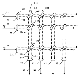
Figure 8 describes an RNS implantation of the DBF
function forming a set of channels 93, 94 (beams formed
in reception, excitation signals for the radiating
elements formed in transmission) for a set of inputs
71, 72, 73 (signals from the radiating elements in the
reception case, signals associated with the beams to be
generated in transmission). The vector converters 30,
31, 32 are connected between the functional inputs 71,
72, 73 and a number of computation planes integrating
combiner arrays (501, 502, 503, ..), (511, 512, 513,
...). Each vector converter comprises an input channel 71
in integer representation and a number of output
channels for the components 722, 721 in residue
representation. The functional input 71 is connected to
the input of the vector converter 30, the combiner 501
is linked to the first output channel 722 of the
converter and the combiner Sll is linked to the second
output channel 721 of the converter. The combiners 501
form part of a first combiner array (501, 502, 503, ...)
making it possible to process data in a first data
format in residue representation. The combiner 511
forms part of a second combiner array (511, 512,
513, ¨) making it possible to process data in a second
data format in residue representation.
CA 02776897 2012-04-05
WO 2011/042348 - 19 -
PCT/EP2010/064508
The first combiner array is connected as follows. An
input channel of the combiner 501 is linked to an
output channel of the converter 30 and an output
channel is connected to an input channel of the
combiner 502. An input channel of the combiner 502 is
linked to an output channel of the converter 31 and an
output channel of the combiner 502 is linked to an
input channel of the combiner 503. An input channel of
the combiner 503 is linked to an output channel of the
converter 32 and an output channel 91 of the combiner
503 is linked to an input channel of the inverse
converter 40. Another combiner array is arranged
similarly with the converters 30, 31 and 32 and the
inverse converter 40. The channel 1 generated by the
DBF function, obtained from the inverse converter 40,
is formed by means of the abovementioned combiner
arrays, each of the arrays independently processing
data in a distinct format.
Other beams can be generated from the same functional
inputs 71, 72, 73 contributing to the forming of the
channel 1. For this, for each of the channels, a number
of combiner arrays are implemented and linked to the
other combiner arrays belonging to one and the same
computation plane. For example, three other channels
are derived from the inverse converters 41, 42 and 43
and, for each of the channels, a number of combiner
arrays, processing data of distinct formats
corresponding to the different computation planes, are
arranged in the same way as the arrays forming the
channel 1. The combiner arrays contributing to
different channels and belonging to one and the same
computation plane are interconnected, either by a
direct distribution from each RNS component of the
vector converters to all the associated combiners, or
by propagation of each component step by step between
adjacent combiners, as illustrated in figure 8. For
CA 02776897 2012-04-05
WO 2011/042348 - 20 -
PCT/EP2010/064508
this, an output channel 723 of the combiner 501 is
linked to an input channel of the combiner 504
contributing to the forming of the channel 2, and so on
for the adjacent combiner arrays. The combiners 502,
503, 511, 512, 513 are also connected to other
combiners belonging to combiner arrays intended to form
other channels from the same functional inputs 71, 72,
73.
More generally, the combiners associated with one and
the same computation plane, with a set of functional
inputs, and for the forming of one and the same
channel, are interconnected to accumulate the partial
terms and constitute a combiner array. The combiners
belonging to different computation planes do not share
interconnections. The combiners processing data of the
same format and contributing to the forming of
different channels from the same functional inputs are
interconnected to propagate the RNS components of the
functional input signal.
These different combiner arrays perform processing
operations independently and in parallel, on reduced
partial dynamics. They can be implanted on integrated
circuits or on different electronic equipment items,
the digital processing operations associated with one
and the same functional input then being able to be
distributed over distinct equipment items. According to
another hardware organization, the processing
operations are divided up by channel and/or sets of
functional inputs in order to integrate all the RNS
components within one and the same integrated circuit
or electronic equipment item, to reduce the development
costs without sacrificing modularity. Specific
equipment items integrate the vector converters and the
inverse converters, in particular in the case of
complex DBF antennas, with a large number of radiating
elements, for a large number of beams, in wideband
CA 02776897 2012-04-05
WO 2011/042348 - 21 -
PCT/EP2010/064508
mode. All these electronic equipment items (vector
converters, inverse converters and DBF processing
operations) then comprise interfaces characteristic of
data in residue representation, with components on
specific dynamics, corresponding to coprime moduli.
As illustrated in figure 3, the conventional DBF
antennas comprise a single combiner array for each
channel (1101, 1201), (1102, 1202), (1103, 1203), the
array processing data in conventional integer
arithmetic on dynamics of 10 to 16 bits or more. With
an embodiment according to the invention, the
implementation of the DBF processing operations is
divided up over a number of independent computation
planes with partial dynamics reduced to a few bits,
which makes it possible to greatly reduce the density
of interconnections at the logic operator level. This
advantageously results in a lesser surface complexity,
a simplified placement and routing of the integrated
circuits, a lesser dissipation and a higher operating
frequency.
Another significant advantage, resulting from the
dividing up of the processing operations on computation
planes with greatly reduced partial dynamics, relates
to the finer granularity of implantation of the
combiners, in terms of surface complexity, of
dissipation and of throughput at the interfaces. The
gain in implantation granularity allows for a better
use of the hardware resources to jointly reduce the
complexity and the dissipation of the DBF function.
In the case of reflector or lens antennas, this
advantage can be amplified by grouping together by
circuit the processing operations relating to a set of
channels (beams in reception, radiating elements in
transmission) formed from shared functional inputs
(radiating elements in reception, beams in
CA 02776897 2012-04-05
WO 2011/042348 - 22 -
PCT/EP2010/064508
transmission). In practice, by thus pooling the
interfaces, the distribution of the functional input
signals is then achieved at the board level and within
processing integrated circuits. This makes it possible
to even further relax the throughput limitation at the
interfaces of the circuits. Figure 9 represents an
example of pooling of the radiating elements by the
embodiment of the invention. The array of twenty nine
radiating elements 13, 14, 15, ... makes it possible to
form five beams corresponding to the focal spots 60,
61, 62, 63, 64. By integrating the combiners associated
with these five adjacent beams in one and the same
ASIC/FPGA circuit, for one or more computation planes,
this represents an average throughput of data at the
input corresponding to 5.8 radiating elements for each
beam, assuming 7 radiating elements for each
independent beam. This hardware organization therefore
makes it possible to integrate a greater number of
combiners for each integrated circuit, given the
throughput limitation at the interfaces, for a reduced
overall complexity and dissipation.
Depending on the need to be satisfied in terms of
quantity of beams, radiating elements and processed
bandwidth, and depending on the integration capacity of
the ASIC/FPGA technology selected, the implementation
according to the invention of the DBF function can make
it possible to integrate processing operations of at
least one complete computation plane, for all the
channels to be formed, within a single ASIC/FPGA. This
means that the circuit can perform processing
operations on an RNS component, for at least one
functional input and for all the channels formed with
this functional input. In this case, it is no longer
necessary to allocate external interfaces of the
circuit to propagate the functional input signals to
the output, which therefore makes it possible to
further increase the integration of combiner functions,
CA 02776897 2012-04-05
WO 2011/042348 - 23 -
PCT/EP2010/064508
this integration being generally limited by the
capacity in terms of interfaces.
According to the variants of the invention for which
the DBF function forms beams on one and the same
bandwidth, for a DBF antenna in reception, a digital
signal from a radiating element is connected to the
input channel of a vector converter, the output
channels of said converter are connected to the input
channels of a set of combiner arrays, the output
channels of said combiner arrays are connected to the
input channels of an inverse converter, the output of
which produces a beam.
According to the variants of the invention for which
the DBF function forms beams on one and the same
bandwidth, for a DBF antenna in transmission, a digital
signal corresponding to a beam to be transmitted is
connected to the input channel of a vector converter,
the output channels of said converter are connected to
the input channels of a set of combiner arrays, the
output channels of said combiner arrays are connected
to the input channels of an inverse converter, the
output of which produces the excitation signal for a
radiating element.
According to an embodiment as represented by figures 1
and 2, the data processing equipment also comprises
data processing means 610 and 660, in addition to the
DBF function, respectively performing the frequency
demultiplexing and multiplexing functions. The vector
conversion and inverse conversion functions can be
arranged according to various organizations around the
DBF function, the frequency demultiplexing and
multiplexing functions so that the latter two functions
are performed on data in vectorized representation or
in conventional representation. According to a first
arrangement in which the frequency demultiplexing and
CA 02776897 2012-04-05
WO 2011/042348 - 24 -
PCT/EP2010/064508
multiplexing functions are performed on data in
vectorized representation, then the data processing
means performing the latter functions are arranged
between the vector converters and the associated
inverse converters. According to a second arrangement
in which the frequency demultiplexing and multiplexing
functions are performed on data in conventional
representation, then the data processing means
performing the latter functions are arranged around the
part of the data processing chain positioned between
the vector converters and the associated inverse
converters.
The implementation of the invention involves the use of
a particular data processing method. For this, the
computation method for forming a beam comprises the
following successive steps in transmission and/or
reception mode:
- conversion of data represented in an integer
format to a data format in residue representation,
- processing of the data from one and the same
vector converter, in parallel and in residue
representation, for the forming of a beam in
reception mode or the excitation signal of a
radiating element of the antenna in transmission
mode,
- inverse conversion of the data in a format in
residue representation to a desired data format.
Detailed studies of antenna hardware architectures
according to the invention have made it possible to
demonstrate a significant reduction in the complexity,
the number of integrated circuits needed, and the
overall dissipation, compared to the existing
solutions. The implementation of DBF functions
according to the invention therefore makes it possible
to satisfy demanding requirements in terms of quantity
of beams, radiating elements and processed bandwidth,
CA 02776897 2012-04-05
WO 2011/042348 - 25 -
PCT/EP2010/064508
by optimizing the hardware complexity and dissipation.
The invention applies to any DBF antenna for space
applications as described in the preferred embodiment,
but also to any onboard applications subject to
complexity and dissipation constraints, notably
telecommunication satellites.