Note: Descriptions are shown in the official language in which they were submitted.
CA 02778042 2012-04-18
WO 2011/035246 PCT/US2010/049499
1
ATTORNEY DOCKET NO. 200591.00091
CARBON NANOTUBE BASED FIELD EMISSION DEVICES AND METHODS
CROSS REFERENCE TO RELATED APPLICATION
[0001] The present application is being filed with the U. S. Receiving Office
as a PCT
application claiming priority from and any other benefit of U.S. Provisional
Patent Application
Serial No. 61/243,612 filed September 18, 2009. The present application also
is a Continuation-
in-Part application of U.S. Patent Application Serial No. 11/428,185 filed on
June 30, 2006, the
entire disclosure of which is hereby incorporated by reference.
TECHNICAL FIELD
[0002] Certain embodiments of the present invention relate to carbon
nanotubes. More
particularly, certain embodiments of the present invention relate to carbon
nanotubes based field
emission devices.
BACKGROUND
[0003] There have been efforts to produce field emission displays (FED), which
provide a
flat panel display using large-area field electron sources to provide
electrons that strike colored
phosphor to produce a color image. FED's combine the advantages of CRTs, such
as providing
high contrast levels and very fast response times, while providing the
advantages of flat panel
technologies. They also offer the possibility of requiring less power, about
half that of an LCD
system for example. An FED display operates similar to a conventional cathode
ray tube (CRT)
with an electron gun that uses high voltage to accelerate electrons which in
turn excite the
phosphors, but instead of a single electron gun, a FED display contains a grid
of individual
nanoscopic electron guns. In the past, an FED screen was constructed by laying
down a series of
metal stripes onto a glass plate to form a series of cathode lines. A series
of rows of switching
gates is formed at right angles to the cathode lines, forming an addressable
grid. At the
intersection of each row and column a small patch of emitters are deposited.
The metal grid is
laid on top of the switching gates to complete the gun structure. A high
voltage-gradient field is
CA 02778042 2012-04-18
WO 2011/035246 PCT/US2010/049499
2
created between the emitters and a metal mesh suspended above them, pulling
electrons off the
tips of the emitters. This is a highly non-linear process and small changes in
voltage will quickly
cause the number of emitted electrons to saturate. The grid can be
individually addressed but
only the emitters located at the crossing points of the powered cathode and
gate lines will have
enough power to produce a visible spot, and any power leaks to surrounding
elements will not be
visible. The grid voltage sends the electrons flowing into the open area
between the emitters at
the back and the screen at the front of the display, where a second
accelerating voltage
additionally accelerates them towards the screen, giving them enough energy to
light the
phosphors. Since the electrons from any single emitter are fired toward a
single sub-pixel,
scanning electromagnets are not needed.
[0004] Although shown to be a viable display technology, past efforts have not
produced
displays which would allow use in commercial products. In FED devices, strong
electric field and
high temperature can cause electron emission from a material. In contrast to
conduction current, emission
current may be low, but the energy of electrons is much higher in emission
than in conduction, thus
making them useful for a number of applications, like displays or electron
microscopy. Emission from
flat metal electrodes require very high voltages at room temperatures. On the
other hand, sharp needle-
like cathodes require lower voltages due to enhancement of electric fields at
the tip of an electrode. An
example of a sharp material for electron emission are carbon nanotubes. Carbon
nanotubes have unique
electrical and mechanical properties. Emission from a single carbon nanotube
starts at a much lower
voltage than a corresponding metal wire of similar dimensions. It has been
suggested that the carbon
nanotubes have atomically sharp wires dangling from its ends or tips. As
compared to a single carbon
nanotube, an array of carbon nanotubes' threshold voltage is much higher and
its emission current
decreased by a large amount.
[0005] There have been efforts to use carbon nanotubes (CNT) in such displays
or other FED
applications. For example, companies like Motorola, Samsung and Cendescent
have shown small
VGA FED type prototypes in various technical meetings (e.g. Motorola's "Nano-
emissive
display, 5" diagonal and 3.3 mm thick). However, there are many challenges to
achieve uniform
field emission from a large area of aligned CNT. In prior efforts, the
synthesis of large area
aligned CNT with uniform height was not achievable. In such efforts, longer
CNT are closer to
the anode than the smaller CNT. Therefore emission current from different
sections of CNT
CA 02778042 2012-04-18
WO 2011/035246 PCT/US2010/049499
3
cathode may be different. Additionally, stray carbon nanotubes may get pulled
out of the array
forming a resistive contact with the anode, which causes short-circuiting. An
additional
limitation relates to a screening effect. It has been suggested that the
threshold voltage increased due
to a screening effect. The screening effect can be thought of as a reduction
in an effective electric field at a
tip of a needle when other needles with similar potentials are placed within
its proximity. Current density
achieved from macroscopic samples of carbon nanotubes are of the order of
lmA/cm2. The emission
current from single carbon nanotube of 10 nm diameter was 1 mA. This means
that only one thousand
carbon nanotubes are effectively emitting from an area of 1 cm2, as compared
to 108 carbon nanotubes
present. Therefore, a need exists for a field emission display that is more
efficient. Due to
proximity of neighboring CNTs, electron emission from an array of CNT occurs
at much higher
voltages as compared to single CNT. This is disadvantageous because higher
voltages are then
required for desired emission from a CNT array to produce the pixel or sub-
pixel brightness or
other characteristics as desired. Efforts to overcome these challenges have
resulted in different
techniques being used, such as like dispersing CNT with an organic binder or
screen printing of
the CNT array. These methods can create uniform coatings of CNT. However,
using these
techniques, aligned CNT cathodes cannot be generated. Therefore, a need exists
for a field
emission display that is more efficient.
[0006] Further limitations and disadvantages of conventional, traditional, and
proposed
approaches will become apparent to one of skill in the art, through comparison
of such systems
and methods with the present invention as set forth in the remainder of the
present application
with reference to the drawings.
SUMMARY OF THE INVENTION
[0007] An embodiment of the present invention comprises a method of
fabricating a cathodic
portion of a field emission display includes the steps of producing an array
of substantially
parallel carbon nanotubes attached at one end to a substantially planar
substrate. Then,
embedding the nanotubes in a polymer matrix that extends to a plane of
attachment of the
nanotubes to the planar substrate, wherein the polymer matrix allows an end of
the nanotubes
distal from the ends attached to the planar substrate, uncovered by the
polymer matrix in
CA 02778042 2012-04-18
WO 2011/035246 PCT/US2010/049499
4
order to allow electrical contact with each other and with an attached
conductor. Next,
detaching the array from the planar substrate, thus producing a surface having
the formerly
attached ends of the nanotubes substantially in a plane, and then attaching
the conductor to
the array of nanotube ends, uncovered by the polymer matrix and distal to the
plane.
[0008] Another embodiment of the present invention comprises a field emission
device that
includes a polymer matrix, wherein the polymer matrix is polysiloxane, and at
least one carbon
nanotube. The at least one carbon nanotube is substantially parallel to one
another. Moreover,
the at least one carbon nanotube is attached to the polymer matrix and an
unattached portion
of the at least one carbon nanotube is substantially level with one another.
[0009] In a further aspect, the invention describes a system and method for
providing a
system and method for emission from a CNT array at low threshold voltages,
wherein alignment
of the CNT array in a desired manner provides such capabilities. In the
invention, the system and
method utilize the synthesis of an aligned array of CNT with uniform height
using a composite
structure formed of aligned CNT and one or more polymers. The system and
method provides a
uniform CNT array. Incorporation of polymer in between CNTs also results in
reducing
screening effect, thus allowing lower threshold voltages (for example
0.5V/micron). There is
also provided a process for forming large area aligned carbon nanotube (CNT)
structures with
substantially uniform height. These aligned CNT structures may be used as a
cathode for field
emission displays (FED). FED have many advantages over current display
technologies based on
LCD and plasma for example. As compared to other technologies for creating
large area CNT
cathodes for FED based on CNT dispersed in organic binders, the aligned CNT
structures of the
present invention have higher electron emission efficiency than dispersed
CNTs. To create a
large area of aligned CNT with substantially uniform height, a composite
structure of CNT and
polymers is formed such that substantially uniform electron emission on large
area can be
achieved.
[0010] These and other features of the claimed invention, as well as details
of illustrated
embodiments thereof, will be more fully understood from the following
description and
drawings.
CA 02778042 2012-04-18
WO 2011/035246 PCT/US2010/049499
BRIEF DESCRIPTION OF THE DRAWINGS
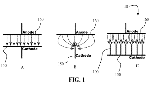
[0011] Fig. 1 illustrates a schematic of field lines, wherein (A) shows
electric field lines for
parallel plate geometry, (B) shows geometry of field lines when cathode is
pointed needle like.
Electric field lines are more concentrated at the tip pf cathode, and (C)
shows when a lot of
needle like cathodes are present;
[0012] Fig. 2 illustrates carbon nanotubes being transferred onto a polymeric
matrix so that the
uniform surface is exposed on the top, wherein (A) carbon nanotubes (CNTs) are
grown on a silicon
wafer, (B) the grown wafer is then inverted onto a polymeric matrix with an
adhesive layer on top of
it, and (C) the silicon wafer is then removed and the carbon nanotubes
transferred onto the polymer
matrix;
[0013] Fig. 3A - 3C show an apparatus for forming the FED type of device
according to the
invention, partially embedding the CNT array into a polymer matrix and CNT
arrays in a
polymer matrix respectively, according to examples of the invention;
[0014] Fig. 4 illustrates how transferring carbon nanotubes onto a polymeric
substrate allows
for the incorporation of a suitable dielectric material in between the
nanotubes without covering the
tips of the nanotubes;
[0015] Fig. 5 illustrates carbon nanotubes being pulled off towards an anode
under high
electric fields;
[0016] Fig. 6 illustrates a patterned carbon nanotube surface;
[0017] Fig. 7 illustrates a flexible device, wherein the anode and the cathode
are
constructed on flexible substrates and patterned suitably and the anode and
the cathode would
then be separated using a sequence of spacers such that the whole geometry is
flexible but
wherein the region between spacers is rigid enough to prevent short circuiting
of the anode and
the cathode;
[0018] Fig. 8 illustrates (A) a typical V-I curve for a vertically aligned
carbon nanotube
sample, (B) plot of ln(I/V2) vs. 1/V, as derived from Fowler-Nordheim
equation, wherein the
enhancement factor can be derived;
CA 02778042 2012-04-18
WO 2011/035246 PCT/US2010/049499
6
[0019] Fig. 9 illustrates a number of threshold voltage measurements;
[0020] Fig. 10 illustrates the Voltage (Volts) and Current ( A) relationship
between four
consecutive runs in air;
[0021] Fig. 11 illustrates emissions from carbon nanotubes grown directly on
aluminum
substrates;
[0022] Fig. 12 illustrates an energy dispersive X-ray spectroscopy (EDAX) from
carbon
nanotubes entrapped in a poly (di methyl siloxane) (PDMS) matrix; and
[0023] Fig. 13A - 13C show photographs of examples according to the invention.
DETAILED DESCRIPTION
[0024] Fig. 1 illustrates a schematic of field lines, wherein (A) shows
electric field lines for
parallel plate geometry, (B) shows geometry of field lines when cathode is
pointed needle like.
Electric field lines are more concentrated at the tip pf cathode, and (C)
shows when a lot of
needle like cathodes are present. Fig. 1(C) also shows the field lines being
divided at the tips
of all the cathodes, thus reducing the enhancing effect. In an embodiment of
the present
invention, rigid and flexible field emission devices and/or systems 10 may be
based on vertically
aligned and non-aligned carbon nanotubes (CNT) 100. Moreover, the field
emission devices 10 may be
patterned or non-patterned vertically aligned carbon nanotubes 100, which may
offer certain advantages.
[0025] Embedding the aligned nanotubes 100 in a polymer matrix 120, a polymer
with a
suitable viscosity may be desired. In such a case, the viscosity should be
such that the polymer
network is of a tackiness nature. The tackiness nature will allow ends of the
carbon nanotubes
100 to penetrate in the network. However, the polymer should be high enough so
that the
polymer chains do not cover the top of the carbon nanotube chains. The
embedding process
involves having the polymer in a partial liquid state prior to embedding and
then in a solid state
thereafter. In this way, there is formed a carbon nanotube array which is not
completely
submerged in a polymer matrix. In this manner, more than only a few strands of
carbon
nanotubes are active and the resulting structure will have high efficiency
since many carbon
CA 02778042 2012-04-18
WO 2011/035246 PCT/US2010/049499
7
nanotubes are active. The structures are also therefore suitable for use in
display technology,
where uniform emission over large area is required. The process or the
invention will allow
production of large areas of active carbon nanotube ends for field emission.
The process of the
invention also provides for and allows robust structures to be formed, where
individual carbon
nanotubes are not pulled out of the structures upon application of voltage or
other deterioration
of the structure during use. For example, multiple hysteresis I-V cycles have
been measured on
the structures to yield uniform results.
[0026] An example of an embedding process of the carbon nanotubes 100 includes
having a pre-
polymer, e.g. poly (di-methyl-siloxane), and then cross-linking after
embedding the carbon nanotubes 100
into a matrix. Then, a monomer, e.g. cyanoacrylate, embeds the carbon
nanotubes 100 in the pre-
polymer film, which then lets the pre-polymer polymerize to form a solid
polymer. A next step
may include dissolving the solid polymer with a solvent to form a viscous
solution. Then, coating the
viscous solution on a rigid substrate, which embeds the carbon nanotubes 100
in the rigid substrate then
and letting the solvent evaporate. An example of this is shown by poly (methyl-
meth-acrylate) in toluene.
Chemical reactions between the two components will then yield a solid
substrate, e.g. epoxy
resins. Softening of a thermoplastic by heating the thermoplastic above its
glass transition
temperature and embedding nanotubes in the softened polymer matrix 120
followed by cooling
of the system.
[0027] With reference to Fig. 2, there is illustrated carbon nanotubes 100
being transferred
onto a polymeric matrix 120 so that the uniform surface is exposed on the top,
wherein (A) the
carbon nanotubes (CNTs) are grown on a silicon wafer 110, (B) the grown wafer
is then inverted
onto the polymeric matrix 120 with an adhesive layer on top of it, and (C) the
silicon wafer 110 is
then removed and the carbon nanotubes 100 transferred onto the polymer matrix
120. Fig. 2
demonstrates how transferring the carbon nanotubes 100 into the polymeric
matrix 120 helps attain a
more uniform upper surface. As the grown carbon nanotubes 100 may not be
absolutely uniform
with respect to one another. Some areas may have longer nanotubes 100, while
other areas may have
shorter nanotubes 100. The effect can reduce the efficiency of the whole
system 10 because
emissions may occur only from a few points, nanotubes 100. The end of the
nanotubes 100 facing
the silicon wafer 110 has a higher surface uniformity, as shown in Fig. 2.
CA 02778042 2012-04-18
WO 2011/035246 PCT/US2010/049499
8
[0028] Embedding carbon nanotubes 100 in the polymeric matrix 120 helps reduce
a
screening effect, which also keeps emissions occurrences at a lower turn on
voltages. Another
effect of embedding carbon nanotubes 100 include assisting in counteracting
surface roughness
and may also yield a more uniform emitting surface, as shown in Fig. 2.
Embedding carbon
nanotubes 100 in the polymeric matrix 120 also helps prevent pullout of the
carbon nanotubes
100 from a base, the polymeric matrix 120, as shown in Fig. 5. In certain
instances, in the
presence of a high electric field, carbon nanotubes 100 may get pulled towards
an anode 160,
which may then lead to a short-circuit. By trapping the carbon nanotubes 100
in the polymeric
base, the carbon nanotubes 100 would be prevented from being pulled off the
base. Moreover,
depending on the desired application, the field emission device 10 may be
flexible or rigid.
The process described above may also create a structure that is super-
hydrophobic, which
would impart self-cleaning abilities to the whole system.
[0029] Turning to Fig. 3A, there is shown a schematic sketch of an instrument
that may be
used for creating uniform arrays of carbon nanotube structures according to
aspects of the
invention. The instrument may include a picometer motor coupled with a vacuum
tweezer
arrangement which uses differences in atmospheric pressure to grasp the CNTs
or array thereof.
Predetermined vacuum tweezer tips may be used to handle the CNT materials in
the desired
manner. In this example, a CNT array is pressed in the polymer matrix or film
such that a
predetermined amount (for example 20 microns) of the CNT array is
substantially uniformly exposed
from the polymer matrix. As seen in Fig. 3B, the array of grown CNT is pressed
into the polymer matrix
to form a uniform surface of exposed CNT. Transferring carbon nanotubes into
the polymeric matrix
helps attain a more uniform upper surface. As grown carbon nanotubes may not
be absolutely uniform at
the surface, with some areas having longer nanotubes than other areas, such an
uneven surface would
reduce the efficiency of the whole system because emission may be occurring
only from a few points. The
other end of nanotubes that faces the substrate has a much higher surface
uniformity. Carbon nanotubes
maybe transferred onto a polymeric matrix in a way that the uniform surface is
exposed on the top. The
instrument may also counteract unevenness of the aligned carbon nanotube
geometry. The instrument
controls the pitch of motion and the motor height such that the exposure of
the entire CNT array can be
controlled. Once the polymer is cross-linked, the CNT array is peeled from the
substrate to expose the
CNT arrays. This may also facilitate creating large area structures with
substantially uniform height of
CNT exposure. In this example, it is also noted that a large area of aligned
carbon nanotube electrodes can
be generated without the need to grow them on large areas. In Fig. 3C, a large
area (such as for example
CA 02778042 2012-04-18
WO 2011/035246 PCT/US2010/049499
9
10"x12") may be formed using smaller sized carbon nanotube array (such as for
example 2"x3") samples
grown on silicon wafer, which may then be formed into larger structures. The
methods of producing the
CNT arrays and partial embedding into the polymer matrix avoids the possible
movement of the
individual CNTs upon the application of high electric fields as seen in Fig. 5
by inhibiting movement of
any CNT in the polymer matrix once it is fully cross-linked. This in turn
avoids an possible short
circuiting that could occur if movement of the CNT's were not so inhibited.
[0030] Polymeric matrix materials according to the invention may be of any
suitable type,
wherein polymeric polymer precursors may include monomers, dimers, trimers or
the like.
Monomers utilized in this invention may generally be selected from the family
of vinyl
monomers suitable for free radical polymerization under emulsion conditions.
Non-limiting
examples of suitable vinyl monomers include methacrylates, styrenes, vinyl
chlorides,
butadienes, isoprenes, and acrylonitriles, polyacrylic and methacrylic esters
and any other
suitable precursor materials. The matrix polymer may be a polymer of one or
more of the
following monomers: methyl methacrylate (MMA), other lower alkyl methacrylates
(e.g. ethyl
methacrylate, propyl methacrylate, isopropyl methacrylate, butyl methacrylate,
2-ethylhexyl
methacrylate, etc., as an example. A starting monomer formulation may also
include one or more
polymerization initiators. These include, for example, benzoyl peroxide,
lauryl peroxide,
azobis(isobutyronitrile ), 2,2'-azobis(2,4-dimethyl-4 methoxypropionitrile),
and 2,2'-azobis(2-
methylpropionitrile) or other suitable initiator materials. These are used in
small amounts which
are well known in the art. Any initiator that is suitable for free radical
polymerization can be
considered according to the invention. Further, the polymer matrix may also be
modified using
nanofillers as an example. Nanofillers are fillers having at least one
dimension in the nanoscale
(1-999 nm). Suitable fillers may include, without limitation, clay minerals,
fibers, micro-spheres,
and layered silicates. Such nanofillers may have their surfaces modified by
surface
functionalization with ionic groups or the like to provide desired interaction
in the polymer
matrix. Additional optional components may be present in the polymer matrix if
desired, such as
chain transfer agents, which are typical of free radical polymerizations, to
facilitate the
polymerization of the monomer or other polymerizable components. Other
optional components
that may facilitate use in various applications may include colorants, mold-
release agents, and
other known modifiers. The starting monomer formulation or mixture may also
include a
crosslinking agent, as for example ethylene glycol dimethacrylate or other
difunctional (i.e.,
CA 02778042 2012-04-18
WO 2011/035246 PCT/US2010/049499
diolefinic) monomer or mixture thereof. The polymeric materials may also be
thermoset plastics
or other suitable epoxy type materials. Epoxy resins useful in the present
invention can be
monomeric or polymeric, saturated or unsaturated, aliphatic, cycloaliphatic,
aromatic or
heterocyclic, and they can be substituted if desired with other substituents
besides the epoxy
groups, e.g., hydroxyl groups, ether radicals, halogen atoms, and the like.
Also, as will be
described in relation to other embodiments, materials such as silicones may be
used to integrate
carbon nanostructures therein, such as poly(dimethylsiloxane) or PDMS. Many
other suitable
polymeric materials are contemplated as will be understood by those skilled in
the art.
[0031] With reference to Fig. 6, there is illustrated a patterned carbon
nanotube surface
170. A few of the benefits of micro-patterning nanotubes 170 include achieving
higher current
densities, as opposed to larger patterned nanotubes 170. Patterning increases
the number of
edges on carbon nanotube films. Having a larger number of edges increases
emission density
from the edges on the carbon nanotube films. Suitable pattern sizes and shapes
may be
prepared for any desired application. Spacing between CNT pillars may allow
for maximizing
the edge effect to increase current density. This could be achieved by
reducing the size of the
pattern. Increasing the edge and spacing between patterns would reduce the
carbon nanotubes
density to thereby reduce the effective emission current per unit area.
Patterning may be
facilitated in a variety of methods, such as depositing a catalyst in a
desired pattern using
photolithography and then growing carbon nanotubes 100 from the desired
patterns. These
patterned nanotubes 170 are then transferred onto a polymeric matrix 120 as
described above.
Another method of patterning includes using soft lithography, wherein stamps,
such as
poly(dimethyl-siloxane) stamps, are used to deposit a catalyst onto desired
regions and wherein
the carbon nanotubes 100 grown from those regions are then transferred to the
polymeric matrix
120 as described above. Using a soft lithography adhesive substance and then
placing it upon a
substrate is another method of patterning that creates a desired pattern. The
carbon nanotubes
100 can then be transferred to the patterned adhesives. Adhesive films may
also be formed on
a substrate while certain regions are masked using conducting or insulating
ink. Then the
carbon nanotubes 100 can be transferred to be partially embedded into the
polymer matrix as
discussed above.
CA 02778042 2012-04-18
WO 2011/035246 PCT/US2010/049499
11
[0032] The processes and methods described above may also be used to change
the whole
geometry of the field emission device 10, such as making the field emission
device 10 flexible
or rigid, depending on the type of polymeric material is used. Embodiments of
the present
invention may include a poly(cyanoacrylate) film on glass that may provide a
rigid emission
device 10 and a poly(di-methyl-siloxane)(PDMS) elastomer that may provide a
flexible
emission device 10.
[0033] In the case of the poly(cyanoacrylate) embodiment, a thin film of
cyanoacrylate
monomer coats a glass slide, preferably in a nitrogen environment with little
moisture. The
film is then left alone for about 10 to 40 seconds so that cyanocrylate
polymerizes partially form
poly(cyanoacrylate) of a low molecular weight. Carbon nanotubes 100 may be
grown on
silicon substrate, which is then pressed lightly on the film, such that ends
of the carbon
nanotubes 100 are partially trapped in the cyanoacrylate. The monomer is then
polymerized in
presence of moisture from the surrounding air to form a rigid film. The
thickness and
smoothness of the film can be controlled by spin coating the film in a
nitrogen atmosphere.
Viscosity of the cyanoacrylate can be controlled by dissolving the
cyanoacrylate in a suitable
ketone, e.g. acetone.
[0034] In the case of the flexible elastomer PDMS film embodiment, a PDMS pre-
polymer
and a catalyst are thoroughly mixed and a resultant film eased onto a suitable
substrate. The
film is then kept on a flat surface for about 2 to 4 hours, in order to let
the film flow and
smoothen the surface. In an example, the film is then heated to approximately
60 C for about
1 to 2 minutes. At this point, tackiness of the film may be checked. The film
should preferably
be tacky, but the film should not be a liquid-like consistency. Vertically
aligned nanotubes 100
grown on silicon (Si) wafers 110 are then inverted onto a top portion of the
partially cross-
linked PDMS film. The whole system is then heated up to about 70 C for about 3
hours. The
Si wafer is then peeled off the substrate, leaving aligned nanotubes 100 that
are trapped in the
PDMS substrate.
[0035] Another aspect of the present invention includes electrically
connecting aligned
nanotubes 100 at one end. The aligned nanotubes 100 have a curvy geometry.
Thus, the
aligned nanotubes 100 have electrical contact with the neighboring nanotubes
100, which may
CA 02778042 2012-04-18
WO 2011/035246 PCT/US2010/049499
12
mean that all the nanotubes 100 are electrically connected. To provide a
better electrical
connection, a metal was deposited onto an end of the nanotube 100 before
transferring the
nanotube 100 into a polymer substrate. Additionally, the carbon nanotubes 100
may be grown
directly onto metallic surfaces. For example, the vertically aligned nanotubes
100 may be
grown on an aluminum substrate. The carbon nanotubes 100 may also be grown on
a stainless
steel substrate. Thereafter, emission properties may be tested with respect to
the emission
device 10.
[0036] In another embodiment of the present invention, rigid anodes 160 and
rigid cathodes
150 may be utilized. The completely rigid system 10 may be synthesized using
the rigid
cathode 150. For example, carbon nanotubes 100 may be grown on a metallic
substrate, e.g.
aluminum or stainless steel. The carbon nanotubes 100 may also be grown on a
silicon wafer
110 or the carbon nanotubes 100 may be grown on the silicon wafer 110 and the
transferred
onto a rigid polymeric substrate as described above. A suitable spacer 140,
e.g. Teflon spacer,
may be used to separate the anode 160 and the cathode 150. A voltage is then
applied and an
emitted current is then measured. An embodiment of the present invention also
includes a
rigid anode 160 and a flexible cathode 150. The rigid anode 160 may be a glass
such as an
indium tin oxide (ITO) coated glass. To create the flexible cathode 150, the
carbon nanotubes
100 is transferred into a flexible matrix using the processes as described
above. Teflon spacers
may also be used. Another spacer 140 that may be used is double sided scotch
tape, which
may be used to create a space between the anode 160 and the cathode 150.
[0037] A completely flexible geometry of an embodiment of the present
invention may also
be synthesized by having both an anode 160 and a cathode be flexible 150. The
flexible
cathodes 150 may be prepared by using the processes as described above. The
flexible anode
160 may be synthesized by depositing aluminum or another metal onto a flexible
matrix using
physical vapor deposition process. Indium tin oxide (ITO) may then be
deposited onto the
flexible matrix. Using a regioregular poly(3 -dodecyloxythiophene-2,5 -
diyl)(P3 DOT), the
flexible conductive anode 160 may be created. A thin carbon nanotube mesh is
transferred
onto a polymeric substrate to create the flexible conductive anodes 160.
CA 02778042 2012-04-18
WO 2011/035246 PCT/US2010/049499
13
[0038] With reference to Fig. 4, there is illustrated how transferring carbon
nanotubes 100
onto a polymeric substrate 120 may also allow for the incorporation of a
suitable dielectric material
130 in between the nanotubes 100 without covering the tips of the nanotubes
100.
[0039] With reference to Fig. 7, there is illustrated a flexible device,
wherein an anode 160
and a cathode 150 are constructed on flexible substrates and patterned
suitably. The anode 160
and the cathode 150 may then be separated using a sequence of spacers 140 such
that the
whole geometry is flexible but wherein the region between spacers 140 is rigid
enough to
prevent short circuiting of the anode 160 and the cathode 150. The flexible
geometry spacer
140 may be placed accordingly, preferably between the anode 160 and the
cathode 150, so that
the anode 160 and the cathode 150 do not short circuit. The spacers 140 may be
rigid enough
and placed to form a grid in between the anode 160 and the cathode 150 so that
a short circuit
does not occur.
[0040] With reference to Fig. 8, there is illustrated in (A) a typical V-I
curve for a vertically
aligned carbon nanotube sample, (B) plot of ln(I/V2) vs. 1/V, as derived from
Fowler-
Nordheim equation, wherein the enhancement factor can be derived. A curve in
Fig. 8(A)
illustrates current with increasing voltage, while another curve illustrates a
current profile while
voltage is being reduced. Fig. 8(B) also demonstrates that an enhancement
factor of about
10,000 is obtainable. With reference to Fig. 9, there is illustrated a number
of threshold voltage
measurements. Fig. 9 illustrates how the threshold voltage remains relatively
constant over a
number of threshold voltage measurements, which is obtainable with the present
invention.
[0041] With reference to Fig. 10, there is illustrated the Voltage (Volts) and
Current ( A)
relationship between four consecutive runs in air. Fig. 10 demonstrates that
threshold voltage
remains relatively the same for all runs, but that emission current decreases.
The decrease in
emission current may be due to oxidation of carbon nanotube 100 tips in an
oxygen filled
environment. With reference to Fig. 11, there is illustrated emissions from
carbon nanotubes 100
grown directly on aluminum substrates. With reference to Fig. 12, there is
illustrated an energy
dispersive X-ray spectroscopy (EDAX) from carbon nanotubes 100 entrapped in a
poly(di-methyl-
siloxane) (PDMS) matrix 120. PDMS is a low energy substrate and tends to coat
higher energy
surfaces. To transfer the carbon nanotubes structures, a partially crosslinked
PDMS film was used.
CA 02778042 2012-04-18
WO 2011/035246 PCT/US2010/049499
14
The crosslink density was such that the structure was still tacky but has high
enough viscosity to
maintain the carbon nanotubes structures. Fig. 12 demonstrates that the PDMS
has not contaminated
the carbon nanotubes tips.
[0042] In Fig. 13, there is shown photographs of forming carbon nanotubes
arrays in association
with a polymer matrix as described. In this example, in Fig. 13A, the carbon
nanotubes are
transferred on a glass slide using poly(cyanoacrylate). A thin coating of
cyanoacrylate is formed on
the glass slide. Carbon nanotubes structures grown on Si wafer are then
inverted on this coated glass
slide. The cyanoacrylate polymerizes in the presence of atmospheric water to
form solid
poly(cyanoacrylate). The poly(cyanoacrylate) then traps the carbon nanotubes
array on the glass
slide. Fig. 13B shows micropatterned carbon nanotube arrays embedded in a
silver epoxy paste. The
micropatterned structures were formed using a photolithography process, with
individual patterns
sized at 250 m for example. Silver epoxy was coated on an ITO coated glass
slide. The carbon
nanotubes were then transferred onto the ITO using a process as described
above for example. The
process allows an intimate electrical contact of micropatterned carbon
nanotubes to be obtained with
an underlying electrode. In Fig. 13C, another example shows the macropatterned
carbon nanotubes
structures were transferred in a rubber. Poly(dimethylsiloxane) (PDMS) was
used as backing.
[0043] In summary, a method of fabricating a cathodic portion of a field
emission display is
disclosed. The method of fabricating a cathodic portion of a field emission
display includes the
steps of producing an array of substantially parallel carbon nanotubes
attached at one end to a
substantially planar substrate. Then, embedding the nanotubes in a polymer
matrix that
extends to a plane of attachment of the nanotubes to the planar substrate,
wherein the
polymer matrix allows an end of the nanotubes distal from the ends attached to
the planar
substrate, uncovered by the polymer matrix in order to allow electrical
contact with each
other and with an attached conductor. Next, detaching the array from the
planar substrate,
thus producing a surface having the formerly attached ends of the nanotubes
substantially in
a plane, and then attaching the conductor to the array of nanotube ends,
uncovered by the
polymer matrix and distal to the plane.
[0044] The advantages of the process according to the invention as compared to
as grown
CNT include eliminating the need to grow carbon nanotubes on large areas. As
growing uniform
CA 02778042 2012-04-18
WO 2011/035246 PCT/US2010/049499
carbon nanotubes on large area is challenging, the process overcomes any such
limitations. The
invention also helps to reduce the screening effect so that emission occurs at
lower turn on
voltages. Transferring nanotubes in a polymeric matrix helps counteract the
surface roughness
and yield a more uniform emitting surface. Embedding nanotubes in polymeric
matrix facilitates
preventing pullout or movement of carbon nanotubes from the base, such as
under high electric
fields that tend to pull the carbon nanotubes towards the anode, which may
lead to short-circuit
of the whole geometry. By trapping the carbon nanotubes in a polymeric base,
such movement or
pull out is avoided. The whole geometry can be made flexible or rigid
depending on desired
application. The arrangement also facilitates electrically connecting aligned
nanotubes at their
end. Aligned nanotubes have a curvy geometry thus they have electrical contact
with the
neighboring tubes. Thus the whole forest is electrically connected. To make a
better electrical
connection metal was deposited on the ends of nanotube before transferring
them into polymer
substrate. Carbon nanotubes were also grown directly on metallic surfaces. For
example,
vertically aligned nanotubes were grown on Aluminum substrate. Carbon
nanotubes were also
grown on stainless steel substrate and their emission properties tested.
[0045] While the claimed subject matter of the present application has been
described with
reference to certain embodiments, it will be understood by those skilled in
the art that various
changes may be made and equivalents may be substituted without departing from
the scope of
the claimed subject matter. In addition, many modifications may be made to
adapt a particular
situation or material to the teachings of the claimed subject matter without
departing from its
scope. Therefore, it is intended that the claimed subject matter not be
limited to the particular
embodiment disclosed, but that the claimed subject matter will include all
embodiments falling
within the scope of the appended claims.