Note: Descriptions are shown in the official language in which they were submitted.
CA 02778072 2012-05-24
B11/032-0
1
TITLE
Method for the determination of a control scheme for a NPC VSC, in particular
as an
active power filter
TECHNICAL FIELD
The present invention relates, inter alia, to a method for the determination
of a control
scheme for a neutral point clamped (NPC) voltage source converter (VSC) with
at least 3
levels.
PRIOR ART
Shunt active power filters are frequently used to minimize the harmonic
disturbances
created by non-linear loads as they improve the filtering efficiency, and also
solve many
issues arising with classical passive filters. In the design of such a system,
special attention
has to be paid to the load currents, which are. intended to be compensated.
Together with
the modulation strategy employed, the load cutTents are the variables that
determine the
circulating current in the power devices of the selected Voltage Source
Converter (VSC).
Especially in 3-level NPC (Neutral Point Clamped) active filters, the commonly
irregular
load can lead to an uneven loss distribution in the semiconductors of a bridge
leg. As in
every converter, the losses in the most stressed device limit the switching
frequency and
the power capability, and a de-rating of the converter current can become
mandatory to
ensure long term-stability of the system.
The semiconductor chips assembled in a standard commercial 3-level NPC bridge
leg
module are mostly dimensioned and rated neglecting the loss distribution over
the specific
elements. In this manner, clue to the issue of loss distribution, the use of
these devices often
results in an oversized design with expensive and weakly utilized
semiconductor area.
Additionally, modulation schemes used to enhance the system efficiency can
contribute
even more to the uneven loss distribution, increasing the difference of the
operating
,
CA 02778072 2014-11-27
78396-194
temperature of the transistors and diodes inside the power module and/or
broadening their
thermal cycling. The thermal mismatch of components leads to induced thermal
stresses on
the materials within the module and thermo-mechanical damage could arise.
Consequently,
the design of 3-level NPC active filters becomes rather complex as the desired
characteristics of high power density, efficiency and component reliability
could
counteract other.
Due to the unequal distribution of losses and mismatch of junction temperature
distribution
among the bridge-leg's semiconductors, in the special situation of high power
converters,
the use of NPC power modules normally results in low semiconductor
utilization. In this
way, the use of single semiconductor devices, rated differently, are more
indicated to build
the bridge-legs of the converter. NPC systems, employing single semiconductors
similarly
rated, usually have these devices installed in separate heat sinks, in order
to achieve a good
thermal decoupling of the individual components. Unfortunately, the use of
different single
semiconductors and/or separate heating sinks normally results in cost
increases and bulky
systems.
SUMMARY OF THE INVENTION
In order to address the loss distribution issue of the conventional NPC active
filters, while
maintaining a high efficiency of the system, in some embodiments of the
present disclosure, a space
vector modulation scheme incorporating an optimal clamping of the phase is
proposed. With no additional
circuitry to the conventional NPC, for most of the typical industrial loads,
it is shown that active filters
employing standard commercial NPC bridge leg modules can have their losses
well
distributed over the chip dies, leading to only a small difference of their
operating
temperature. In some embodiments, herein also a suitable control concept
capable of balancing
the DC-link voltages and, to some extent, of maintaining the optimal clamping
of the currents, is
proposed.
In this proposal, depending on the current shape of the load compensated by
the active
filter the top and bottom DC-link capacitors are alternately loaded according
to a carrier
signal with 3 or 9 times the fundamental frequency of the grid. Especially for
high
frequency operation, a considerable reduction of losses can be achieved by
clamping the
bridge leg that is closing all upper or middle-leg switches in the bridge leg,
which handles
the highest current values. Increasing the frequency of the clamping carrier
and avoiding
CA 02778072 2014-11-27
78396-194
3
that the switching intervals match the instant: of high current values can
effect a better
controllability of the loss distribution among the bridge leg components. Note
that both
clamping strategies are intended to balance the operating junction
temperatures and/or the
power losses across the transistors (Integrated Gated Bipolar Transistors
IGBTs), while the
total losses of the system are minimized. Accordingly, mainly the operating
switching
frequency needs to be strategically selected. In fact, the loss distribution
across the
components of a bridge leg is strongly dependent on the switching frequency
and DC-link
voltage operation. These variables are proportional to the switching losses,
and they can be
used together with the current clamping scheme to optimally design the active
filter for a
specific semiconductor technology and compensated load.
In some embodiments of the present disclosure, the synchronization of the
carrier modulator with the grid
voltages or load currents is important to perform the clamping during the
desired non-switching intervals.
The optimal current clamping can be previously defined by an accurate analysis
of the necessarily
known load currents. In cases where the displacement of the load current
varies
considerably with the handled power, ,a look-up table can be built to tune the
carrier
according to the instant power processed by the loan. In cases where the load
is unknown,
the clamping strategy can be adapted during operation with an algorithm, which
predicts
the losses across the transistors of one phase leg. The calculation needs to
incorporate the
space vector modulation such that the impact of the current clamping pattern
is considered
correctly according to the compensated load. With the defined modulation
index, the
relative on-times/transitions of the discrete voltage space vectors can be
determined. Thus,
combining this information with the known conduction/switching loss
characteristics of the
employed semiconductors, the averaged conduction and switching losses over one
switching period can be calculated. By storing the loss data calculated in
each switching
period, the mean losses over a fundamental grid period in each transistor
device can be
obtained recursively. Finally, after every switching period, adjustments of
the variables,
directly related to component losses, can be performed in order to equalize
power losses in
these devices (switching frequency, fs, DC-link voltage reference, uDC_ref,
clamping
pattern's duty cycle, D, and phase, cp )
The proposed clamping scheme can be used in other 3-level VSC tppologies, such
as the
T-type VSC as depicted for example in Fig. 1(d).
Operation conditions, such as, under strongly irregular loads, unbalanced DC-
link voltages,
or during loading variations, could make the equalization of power losses
impossible., that
CA 02778072 2014-11-27
' 78396-194
4
is, not only among the bridge leg's components but also between different
phase legs. This
is particularly true because the variables, which constitute the degree of
freedom of the
proposed modulation, are commonly limited to the application requirements
(switching
frequency, fs, DC-link voltage, UDC, semiconductor technology, and the
clamping
pattern). Additionally, the current waveforms in each phase of the 3-level
active filter
VSC are necessarily similar; otherwise,, the poWer losses among the different
phases will
differ. Finally, during unbalanced DC-link voltage conditions, the desired
clamping of the
phase current cannot be always attained due to the required control of the
neutral point
potential.
Basically according to some embodiments the proposed method for the
determination of
control scheme of a voltage source converter, which is neutral point clamped
entails at least
the following steps:
= Positioning of a window of 1200 within the phase cycle of the grid/load
such as to
be positioned around the centre peak maximum of the negative half wave and the
positive half wave of the grid/load. This window defines the time span within
which clamping of the corresponding leg can be allowed.
= Determining the frequency of the clamping carrier modulator to either be
three
times the basic frequency of the grid/load (third harmonic) or nine times the
basic
frequency of the grid/load (ninth harm,onic). This determination can be based
on
visual inspection of the waveform of thesfid/load or it can be based on an
analysis
of the waveform. The higher the frequencies of distortions and the more
distortions
the more likely the higher clamping carrier modulator frequency has to be
chosen.
It can also be based on a simulation or an actual measurement as will be
detailed
further below.
= Once the window and the frequency of the clamping carrier modulator is
determined, the voltage source converter is operated under additional control
of the
clamping carrier modulator in that, depending on the on/off status of the
clamping
earner modulator, the switching in the corresponding leg is interrupted so the
corresponding leg is clamped- this however only if within the above-mentioned
10 window. For if the clamping carrier modulator of the corresponding
leg is
essentially ignored outside of the above-mentioned window, the above-mentioned
window is used for switching on/off the clamping. For additional optimization,
it is
now possible (but not necessary) to adapt further operating parameters in
particular
CA 02778072 2014-11-27
- 78396-194
the phase shift of the clamping carrier modulator with respect to the
grid/load. The
clamping carrier modulator needs to be synchronized to the grid/load, and the
relative phase can be used for optimization, wherein the optimization is
carried out
to lead to an optimum balance and a total loss as low as possible. Further
parameters, which can be adapted in this optional step, will be specified
below.
More specifically, the present invention relates to a method for the
determination of a
control scheme for a neutral point clamped (NPC) voltage source converter
(VSC), typically with 3 phases,
and with at least 3 levels, for example as a shunt active power filter, with a
topology of three bridge legs
between each of three phases of a grid and a neutral point, each leg
comprising at least four active switches.
In some embodiments, particular topologies are to be controlled as illustrated
in figures 1 a, b, and d.
be controlled as illustrated in figures 1 a, b, and d.
According to the invention, there is provided a clamping carrier modulator
synchronized
with the grid for the control of no-switching intervals, said method
comprising at least the
following steps:
i) analyzing the waveform of the grid and/or a load voltage and
determination of windows of 120 within the voltage cycle of the grid/load,
wherein the windows are centered around the positive and negative peak
maximum of the grid/load voltage waveform, said windows defining the
allowed period for no-switching of the corresponding bridge leg;
ii) operating or simulating the operation of the voltage source converter
with a
clamping carrier modulator frequency equal to the third harmonic frequency of
the grid/load, wherein, if within said window, as a function of the clamping
carrier modulator the switching of the corresponding bridge leg is interrupted
and clamped, and then analyzing the balance in the operating junction
temperatures and/or power losses across the active switches and also analyzing
the total losses of the voltage source converter;
iii) operating or simulating the operation of the voltage source
converter with a
clamping carrier modulator frequency equal to the ninth harmonic frequency of
the grid/load, wherein, if within said window, as a function of the clamping
carrier modulator the switching of the corresponding bridge leg is interrupted
and clamped, and then analyzing the balance in the operating junction
temperatures and/or power losses across the active switches and the total
losses
of the voltage source converter;
,
CA 02778072 2012-05-24
B11/032-0
6
iv) comparing the balance and the total losses of steps ii) and iii)
and selecting
either the clamping carrier modulator frequency according to step ii) or step
iii)
showing, as primary criterion, the better balance and, as secondary criterion,
the
lower total losses;
v) operating or simulating the operation of the voltage source converter
with the
selected clamping carrier modulator frequency, wherein as a function of the
clamping carrier modulator the switching of the corresponding bridge leg is
interrupted and clamped in as far as within said window, while iteratively
changing at least one of the following operating parameters of the voltage
source converter: switching frequency, DC-link voltage reference, duty cycle
of
clamping carrier modulator, phase shift of the clamping carrier modulator
relative to the grid, and optimizing the balance in the operating junction
temperatures and/or power losses across the active switches and the total
losses
of the voltage source converter, as a function of the adjustment of these
operating parameters;
until reaching optimum operation parameters for the control scheme.
According to a first preferred embodiment of the proposed method within step
v) initially
the phase shift of the clamping carrier modulator relative to the grid/load
is, preferably
systematically and/or iteratively, adapted to find the optimum balance and/or
total loss of
the voltage source converter.
According to yet another preferred embodiment, the voltage source converter is
adapted to
act as a shunt voltage source converter.
For compensation of imbalances of the DC-link voltage the ratio of no
switching to
switching intervals within the window (3) between the positive half wave and
the negative
half wave of the grid can be unbalanced.
The bandwidth of the current controller (G(s)) used in a corresponding DQ-
frame based
control concept is preferably selected to be at least 20 times, preferably at
least 50 times
higher than for the main DC link voltage controller (H(s)). The bandwidth of
the partial
DC link voltage controller (R(s)) is selected as at least less than one third,
preferably at
least less than one fifth of the main voltage loop.
The voltage source converter can be a 3-level T- type VSC converter or 3-level
A-NPC
VSC converter.
The present invention furthermore relates to a method of operating a voltage
source
CA 02778072 2012-05-24
B11/032-0
7
converter, in particular a shunt active power filter, using a control scheme
as determined as
outlined above.
Preferably the converter is operated at a voltage in the range of 300-10000 V.
preferably in
the range of 500- 1500V or 700-1000 V.
Preferably the converter is operated using a switching frequency in the range
of 100 Hz-1
MHz, preferably in the range of 5 kHz-100 kHz.
Furthermore the present invention relates to the use of a method as outlined
above for the
determination of the control scheme of 3-level VSC adapted to act as a
photovoltaic grid
inverter, a rectifier, or a motor drive.
Further embodiments of the invention are set forth in the dependent claims.
BRIEF DESCRIPTION OF THE DRAWINGS
Preferred embodiments of the invention are described in the following with
reference to
the drawings, which are for the purpose of illustrating the present preferred
embodiments
of the invention and not for the purpose of limiting the same. In the
drawings,
Fig. 1 shows active filters based on: (a) 'Conventional 3-level NPC
VSC; (b) 3-
level A-NPC VSC; (c) 2-level VSC; and (d) 3-level T-type converter;
Fig. 2 shows 3-level active filter modulation schemes: (a) clamping
strategy with
3rd harmonic frequency carrier; (b) clamping strategy with 9th harmonic
frequency carrier; and (c) clamping strategy during imbalanced DC-link
capacitor voltages with 9th harmonic frequency carrier;
Fig. 3 shows the active filter control strategy based on DQ-frame
theory;
Fig. 4 shows a partial DC-link voltage control scheme: (a) balanced
condition; (b)
light imbalanced DC-link voltages, partially preserving clamping; and (c)
high voltage imbalances requiring hysteresis control;
Fig. 5 shows the bridge leg components loss distribution: (a)
conventional
sinusoidal pulse width modulation SPWM; (b) clamping strategy with 3rd
harmonic frequency carrier; and (c) clamping strategy with 9th harmonic
frequency carrier, in each case solid black bars 12 indicate switching losses
(40kHz) and hatched bars 13 indicate conduction losses;
Fig. 6 shows the bridge leg components operating junction temperature:
(a)
CA 02778072 2012-05-24
B11/032-0
8
conventional SPWM; (b) clamping strategy with 3rd harmonic frequency
carrier; and (c) clamping strategy with 9th harmonic frequency carrier;
Fig. 7 shows an efficiency comparison between the different topologies
of 12kVAr
active filters employing commercial semiconductors: (a) clamping strategy
with 3rd harmonic frequency carrier; and (b) clamping strategy with 9th
harmonic frequency pattern; and
Fig. 8 shows the bridge leg components Joss distribution for: (a) 3-
level NPC, and
(b) T-type active filter operating at 40kHz with 3rd harmonic clamping
pattern; and (c) 3-level 1-type active filter operating at 8kHz with 9th
harmonic clamping pattern, in each case solid black bars 12 indicate
switching losses (40k.Hz) and hatched bars 13 indicate conduction losses.
DESCRIPTION OF PREFERRED EMBODIMENTS
The 3-level NPC topology as e.g. shown in Fig. 1(a) is most often used in the
medium
voltage range applications. NPC VSC is an alternative for low-voltage
applications.
Compared to a 2-level VSC (cf. Fig. 1(c)), the 3-level NPC VSC features two
additional
active switches, two additional isolated gate drivers, and four diodes per
phase leg. The 3-
phase NPC VSC allows 27 switch states in the space-vector diagram, whereas the
2-level
allows only eight switch states. Hence, the superior controllability of the
phase currents
and DC-link voltage (UDC) is distinctly advantageous over the 2-level
converter.
Additionally, in applications such as photovoltaie grid inverters, rectifiers,
motor drivers
and active filters, 3-level NPC systems can achieve lower losses than
conventional 2-level
converters if the considered switching frequency is high enough.
Adding up two extra active switches per phase leg of the conventional NPC a
substantial
improvement of loss distribution can be achieved with the additional switching
states and
new commutations possibilities incorporated (cf. Fig. 1(b)). This
configuration, Active
NPC (A-NPC), allows a specific utilization of the upper and lower path of the
neutral tap
and, thus, affects the distribution of conduction and switching losses. When
compared to a
conventional 3-phase 3-level NPC topology, the 3-phase 3-level A-NPC requires
6
additional active switches and 3 extra isolated gate drivers. Therefore, the
main factors
preventing the 3-level A-NPC VSC from being successful in the active filter
market are the
substantial increase of costs and complexity. Note that, when compared to the
conventional
CA 02778072 2012-05-24
B11/032-0
9
2-level VSC (cf. Fig. 1(c)), which is widespread in commercial systems, the A-
NPC
requires 12 extra active switches and isolated gate drives.
One disadvantage of the 3-level topologies is the active control of their
neutral-point
potential. Although under ideal condition, the DC-link capacitor voltages
naturally balance
over one fundamental cycle, asymmetries in the semiconductor characteristics,
different
gate delay time, dynamic load changes, and/or unbalanced loads can cause a
steady drift of
the neutral-point potential. Since the 3-level topology offers redundant space
vectors on the
inner hexagon of the space vector diagram, it is possible to maintain the
stability of the
neutral point potential with no additional circuitry and no additional
switching transitions.
Especially in 3-level active filters, the commonly irregular load can lead to
an uneven loss
distribution in the semiconductors of a bridge leg. As in every converter, the
losses in the
most stressed device limit the switching frequency and the power capability, a
de-rating of
the converter current can become mandatory to ensure long term-stability of
the system.
The semiconductor chips assembled in a standard commercial 3-level bridge leg
module
are mostly dimensioned and rated neglecting the loss distribution over the
specific
elements. In this manner, due to the issue of loss distribution, the use of
these devices often
results in an oversized design with expensive and weakly utilized
semiconductor area.
Additionally to that, modulation schemes used to enhance the system efficiency
can
contribute even more to the uneven loss distribution, increasing the
difference of the
operating temperature of the transistors and diodes inside the power module
and/or
broadening their thermal cycling. The thermal mismatch of components leads to
induced
thermal stresses on the materials within the module and thermo-mechanical
damage could
arise. Consequently, the design of 3-level active filters becomes rather
complex as the
desired characteristics of high power density, efficiency and component
reliability could
counteract each other.
In order to address the loss distribution issue. -of the 3-level VSCs, a space
vector
modulation scheme incorporating an optimal clamping of the phase is proposed.
This
strategy can maximize the efficiency of the system and/or to improve the
distribution of the
component losses, where the variation of power/thermal stress of the
individual elements
in a bridge leg is minimized. Additionally, a suitable control concept capable
of balancing
the DC-link voltages and, to some extent, maintain the optimal clamping of the
currents, is
disclosed.
For the converters presented herein, a space vector modulation scheme
incorporating an
CA 02778072 2012-05-24
B11/032-0
optimal clamping of the phase, as described in B. Kaku, I. Miyashita, and S.
Sone,
"Switching loss minimized space vector pwril Method for igbt three-level
inverter," IEEE
Proceedings. Electric Power Applications, Vol. 144, pp. 182-190, May 1997, is
implemented. The output voltage vector is always formed with the three closest
discrete
5 voltage space vectors. Since the 3-level topology offers redundant space
vectors on the
inner hexagon, it is possible to implement an optimal clamping strategy in
order to reduce
switching losses.
in the disclosed modulation scheme, each phase leg of a 3-level VSC can have
its
switching operation stopped for 120 degrees in one period without degrading
the
10 performance of the system. When aiming for high efficiency during high
operating
frequency, one would naturally avoid switching the phase leg with the highest
current
values, while keeping the loss distribution among the phase legs of the
converter
symmetric. However, during this process the commonly irregular currents of the
active
filter can lead to a strongly uneven power loss distribution across the
semiconductors of a
bridge leg. In cases where standard commercial power modules are used, the
loss
distribution issue can increase the difference ofthe operating temperature of
the transistor
and diodes inside this device and/or broadening their thermal profile, thereby
directly
improving the reliability of these components.
Herein, depending on the current shape of the load compensated by the active
filter the top
and bottom DC-link capacitors are alternately loaded according to a carrier
signal with 3 or
9 times the fundamental frequency of the grid. Fig. 2(a) and 2(b) show both
modulation
strategies adjusted for a 3-phase 12-pulse diode rectifier with constant
output current as
load. Therein, especially for high frequency operation, a considerable
reduction of losses
would be achieved by clamping the bridge leg, which handles the highest
current values
(cf. Fig, 2(a)). By increasing the frequency of the clamping process and
avoiding that the
switching intervals match the instant of high current values, a better
controllability of the
loss distribution among the bridge leg components can be obtained (cf. Fig.
2(b)).
The figures 2, top row, show the above-mentioned window 3, within which no
switching is
allowed, and which is centered around the maximum of the positive half wave
and the
negative half wave (in a) and b) only the window for the positive half wave is
indicated).
In the figure, ILR represents the load current and IR represents the
compensated current.
Non-switching, i.e. clamping of the corresponding leg, is allowed only within
the window
3, depending on the switching state of the modulation carrier 3. This is
illustrated in the
CA 02778072 2012-05-24
B11/032-0
11
bottom row of figure 2. Outside of the window 3 the modulation carrier 1 is
essentially
ignored. If the carrier 1 is on zero level and if one is within window 3
clamping is allowed,
as indicated graphically by the actual no switching intervals 2. Depending on
the phase
shift between the modulator 1 and the grid, the corresponding blocks are
shifted. For
example, if in the left column of figure 2 the carrier is shifted by 5
relative to the grid, one
of the intervals 2 will become 35 , and the other one will become 25 . The
phase shift can
be used for optimization of the balance. In the central column of figure 2
shifting the phase
of the modulator will only lead to a corresponding shifting of the three 20'
intervals until
one of them reaches the end of the 120 window. The same holds true for the
example in
the rightmost column figure 2. The latter example shows how it is possible to
adjust
imbalances in the DC link by differentiating between the clamping in the
positive half
wave and in the negative half wave.
The same modulation carrier is used for all three phases. For symmetry reasons
the three
phases R (second row), S (third row) and T (fourth row) are only shifted by
120 relative to
each other as concerns the compensated current TAFR as well as the voltage
UR,o. The
hatched areas indicate the timespans within which the switching takes place.
Note that both clamping strategies are intended to balance the operating
junction
temperatures and/or the power losses across the transistors (IGBTs), while the
total losses
of the system are minimized. Accordingly, mainly the operating switching
frequency needs
to be strategically selected. In fact, the loss distribution across the
components of a bridge
leg is strongly dependent on the switching frequency and DC-link voltage
operation. These
variables are proportional to the switching losses, and they can be used
together with the
current clamping scheme to optimally design the active filter for a specific
semiconductor
technology and compensated load.
In order to keep the balancing of the DC-link capacitor voltages unaltered and
the loss
distribution among the phase legs of the converter symmetric over one
fundamental cycle,
a proper selection of the redundant zero vectors are required. This condition
is found when
the duty cycle (D) of the carrier is set to 50%. Any other duty cycle value
produces an
asymmetric modulation. It can be used for the balancing control of the DC-link
capacitor
voltages as shown in Fig. 2(c). For D > 50%, the upper DC-link capacitor is
charged while
the bottom capacitor is discharged. When D <50%, the capacitor charging cycle
is
changed.
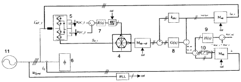
The DQ-Frame based control concept suitable for the 3-level active filters
considered here
CA 02778072 2012-05-24
B11/032-0
12
is shown in Fig. 3. It consists of a fast current control loop and a slow
voltage loop.
Additionally, there is a partial DC-link voltage control, which acts to
balance the DC-link
capacitor voltages. Other strategies, such as PQ theory, Fryze currents,
generalized
integrators, frequency domain strategies (DFT, RDFT and FFT), etc., can also
be
employed.
In order to obtain a good controllability of the active filter currents, the
current controller
(G(s)) bandwidth is selected as fifty times higher than for the main DC-link
voltage
controller (H(s)). Therein, a high voltage control error occurring due to the
small controller
gain can be prevented by increasing the controller gain proportionally to the
error signal. In
order to maintain the optimal clamping of the currents to some extent during
imbalances of
the DC-link voltages, the bandwidth of the partial DC-link voltage controller
(R(s)) is
selected as one fifth (1/5) of the main voltage loop. A non-linear control
combining
hysteresis and linear concepts is employed as shown in Fig. 4. For low voltage
imbalances,
the output signal of the R(s) controller is compared to a PWM modulator with 3
or 9 times
the mains frequency. This determines the carrier duty cycle that selects one
of the
redundant zero vectors on the inner hexagon of the space vector modulation
scheme. For
high voltage imbalances, the modulator saturates and a hysteresis-like control
takes over.
High values for the DC-link capacitors are desired for the voltage variations,
avoiding then
the operation of the hysteresis control.
The synchronization of the carrier modulator with the grid voltages or load
currents is
essential to perform the clamping during the desired non-switching intervals.
The optimal
current clamping may be defined previously by an accurate analysis of the
necessarily
known load currents. In cases where the :rdisplacement of the load current
varies
considerably with the handled power, a look-up table can be built to tune the
carrier
according to the instant power processed by the load. In cases where the load
is unknown,
the clamping strategy could be adapted during operation with an algorithm,
which predicts
the losses across the transistors of one phase leg. The calculation
incorporates the space
vector modulation such that the impact of the current clamping pattern is
considered
correctly according to the compensated load. With the defined modulation
index, the
relative on-times/transitions of the discrete voltage space vectors can be
determined. Thus,
combining this information with the known conduction/switching loss
characteristics of the
employed semiconductors, the averaged conduction and switching losses over one
switching period can be calculated. By storing the loss data calculated in
each switching
,
CA 02778072 2012-05-24
B11/032-0
.13
. = L.:.,
period, the mean losses over a fundamental grid period in each transistor
device can be
obtained recursively. Finally, after every switching period, adjustments on
the variables,
directly related to component losses, can be performed in order to equalize
power losses in
these devices (switching frequency, fs, DC-link voltage reference, uDC_rel,
clamping
pattern's duty cycle. D, and phase, cp).
In order to quantify the feasibility of the proposed loss minimized space
vector modulation,
simulations are performed for a 3-phase 3-level NPC active filter rated to 12
kVAr. This
system operates with a 230Vrms/50Hz grid voltage at 30 kHz switching frequency
and
800V DC-link. The 3-level Trench and Field Stop IGBT power module
F3L5ORO6W1E3_B 1 1 is selected and its loss characteristics and thermal models
are
obtained directly in the datasheet. The loss analyses are performed for
nominal operation
of the active filter with a 3-phase 12-pulse diode rectifier with constant
output current as
load. For comparative purposes, three Modulation schemes are analyzed: the
conventional
SPWM method, in which there is no reduction of switching control; and the two
clamping
strategies proposed, one guided by a carrier signal with 3 (cf. Fig. 2(a)) and
other with 9
(cf. Fig. 2(b)) times the fundamental frequency of the grid.
The resulting averaged power loss distribution and the operating junction
temperature (TJ)
of the individual elements in a bridge leg are shown in Fig. 5 and Fig. 6,
respectively. In
Fig. 6 a constant heat sink temperature (THS) of 80 C is considered in the
analysis. The
system operating with SPWM modulation results in the lowest efficiency, as a
total
semiconductor loss (PT) of 237W exists (79W per power module). By avoiding
switching
currents with high values, the clamping strategies guided by a signal with a
3rd and 9th
harmonic pattern obtain a loss reduction of 16% and 9.3%, respectively.
Additionally, the
operating junction temperatures of the upper/bottom and inner IGBTs or diodes
are well
balanced and symmetric for all bridge legs (cf. Fig 6(b)).
The proposed clamping strategies are intended to balance the operating
junction
temperatures and/or the power losses across the IGBTs, while the total losses
of the system
are minimized. Accordingly, for the disclosed example, the operating switching
frequency
was strategically selected with the aim that for both proposed modulation
schemes these
goals could be successfully attained. In fact, the loss distribution across
the components of
a bridge leg is strongly dependent on the switching frequency and DC-link
voltage
operation. These variables are proportional to the switching losses and they
can be used
together with the current clamping scheme to optimally design the active
filter for a
CA 02778072 2012-05-24
B 11/032-0
14
specific semiconductor technology.
Note that the proposed clamping scheme can be used to other 3-level VSC
topologies, such
as the T-type VSC depicted in Fig. 1(d). In the following section, suitable
shunt active
filters derived from the 2-level VSC, the '3-level NPC and the T-type
converter are
presented. An efficiency comparison between these converters employing the
proposed
space vector modulation scheme incorporating an optimal clamping of the phase
is shown,
for operation in the switching frequency range of 5kH to 50kHz and low DC-link
voltage
level (UDc=800V). A 3-phase 12-pulse diode rectifier with constant output
current is
considered in the loss analyses with switching loss measurements of commercial
semiconductors obtained in a test setup.
A calculation of the efficiency of 2-level and 3-level active filters allowed
a comparison
between the efficiency of a 12kVAr rated 3-phase shunt active filters derived
from the 2-
level VSC, the 3-level NPC, and a T-type converter. A 3-phase 12-pulse diode
rectifier
was considered as load in the loss analyses with switching loss measurements
of
commercial semiconductors obtained on the test setup.
For an accurate analysis of the switching losses,, the information from the
datasheets alone
would not be enough to enable a fair compacison of the studied systems. Due to
the
mismatch of voltage rated devices in the T-type topology, the turn-on energy
of the 1200V
IGBTs will be lower if the commutating diode is only 600V rated because of the
considerably lower reverse recovery charge. In the same matter, the 600V
device turn-on
loss energy will be higher if the commutating diode is 1200V rated.
A calculation of the active filter topologies efficiency yielded that the
efficiency of each
active filter studied here, is determined with an algorithm similar to the one
presented in
M. Schweizer, T. Thiedli, and J. W. Kolar, "Comparison and implementation of a
3-level
npc voltage link back-to-back converter with sic and si diodes," in Proc.
Twenty-Fifth
Annual IEEE Applied Power Electronics Conf. and Exposition (APEC), pp. 1527-
1533,
2010. The calculation incorporates the space vector modulation such that the
impact of the
optimal clamping is considered correctly according to the compensated load.
With a
defined modulation index, the relative on-times/transitions of the discrete
voltage space
vectors can be determined. Thus, the averaged,conduction losses and the
switching losses
over one switching period can be calculated. Finally, the mean losses over a
fundamental
period in each device can be obtained by integrating the corresponding
expressions over
CA 02778072 2012-05-24
B11/032-0
the full mains voltage period.
In Fig. 7 the pure semiconductor efficiency of 12 kVAr shunt active filters
derived from
the 2-level VSC, the 3-level NPC and the T-type converter is presented for
operation in the
switching frequency range of 5kH to 50kHz and low DC-link voltage level
(Upc=800V).
5 in this analysis the loss data of the commercial IG.BTs 1KW25T120 and the
IKW3ON6OT
obtained with the test setup are used for the comparison when a 3-phase 12-
pulse diode
rectifier with constant output current is considered as load. For the
calculation of the 3-
level T-type topology efficiency, the same, algorithm accounting for the
proposed space
vector modulations as for the NPC converter is employed.
10 Due to the fact that the 1200V devices in the T-type active filter are
mostly commuted at
half DC-link voltage instead of the always 800V in the 2-level VSC, the
switching losses
are considerably reduced. Therefore, for low switching frequency values the 3-
level T-type
active filter already shows superior performance than the conventional 2-level
version.
Compared to the 3-level NPC topology, the T-type system has lower conduction
losses, but
15 higher switching losses. In this manner, in both clamping strategies the
efficiency of the T-
type converter is outstanding for up to 10 kHz switching frequency (cf. Fig
7). On the other
hand, for switching frequencies above 10 kHz, the 3-level NPC topology is
superior.
Fig. 8(a) and 8(b) show the bridge leg components mean power loss distribution
for the 3-
level NPC and the T-type active filters operating at 40 kHz switching
frequency.
respectively. As can be observed the overall switch utilization of the T-type
active filter is
extremely low. On the other hand, the 3-level NPC active filter achieves an
outstanding
performance, enabling that all semiconductor. clips for IGBTs or diodes
operate with
similar junction temperatures. For the T-type VSC, the optimum switch
utilization occurs
at low switching frequency (8kHz) and, in the switching frequency range of
5kHz to
50kHz, it can only be reached by the clamping strategy with 9th harmonic
pattern. Fig. 8(c)
shows the T-type active filter performance for this operation.
The strategy proposed here was applied to 3-level active filters; however
other industrial
applications employing 3-level VSCs, such as photovoltaic grid inverters,
rectifiers, motor
drivers, among others can also take advantage of this concept. The modulation
strategy
presented here can also be combined with the active NPC (A-NPC) topology, in
order to
not only improve the loss distribution among the component of the phase leg,
but also to
enhance the efficiency of this system.
CA 02778072 2012-05-24
B11/032-0
16
LIST OF REFERENCE SIGNS
1 Clamping carrier, carrier 13 conduction losses, hatched
modulator bars in Fig, 5
2 actual no switching interval 14 PWM modulator
3 possible no switching interval 15 hysteresis control level
4 space vector modulation 16 control level
active filter 17 2-level
6 nonlinear load 18 3-level T-type
7 partial voltage controller 19 3-level NPC
8 current controller ?CI balanced 1GBT's Tj for 3-
9 voltage controller level NPC
low pass filter 71 bridge leg of R-phase
11 grid 99 bridge leg of S- phase
17 switching losses (30 kHz), 23 bridge leg of T-phase
solid black bars 24 neutral point