Note: Descriptions are shown in the official language in which they were submitted.
CA 02778494 2012-04-20
WO 2011/050225 PCT/US2010/053642
A Direct Mounted Photovoltaic Device with Improved Adhesion and Method
Thereof
This invention was made with U.S. Government support under contract DE-FC G-
070017054 awarded by the Department of Energy, The U.S, Government has
certain rights in this invention.
CLAIM OF PRIORITY
The present application i:iaorns the benefit of the filing date of US
Provisional
Application No:. 61/253r,980 (sled 22 O T- tt9) and 611257 488 (fled 03-Nov-
2OO9
the contents of which are hereby incorporated by reference in their entirety.
FIELD OF THE INVENTION
[001] The re:>ent invention relates to a photovoltaic device and method
thereof
that is directly mounted to a structure, rt oce particularly a photovoltaic
shingle and
method thereof adapted to be directly mounted to building structure such as a
roof
deck or wall,
BACKGROUND
[002] Efforts to improve the state of the art in the area of solar power
generation particularly in the area of building mounted generation has been
receiving ever increasing industry focus over the last few years. A subset of
building
mounted generation is building-integrated photovoltaics 0B V), where the
photovoltaic elements are integral parts of the building (such as providing
exterior
weather skin as in shingles or siding. Of particular importance is the goal of
providing a reliable and durable solar power generation system that provides
the
most kilowatt hours (w) for the least amount of cost. Some of the issues
associated with reaching this goal concern the ability of the generation
system to be
easy to assemble and install, have a relatively high KwH output, and be
durable (eq.
hold up over time given the likely environmental conditions such as relatively
high
winds and rain). One particular issue eiated to iurabili;y is that of wind
loading,
such as determined via (Underwriters Laboratories) UL 1897, Tests for Uplift
Resistance of Roof Assemblies, That is the ability of the system to not be
damaged
when subjected to winds, for example, in excess of 100 riles per hour or more.
One
aÃ-ticdlar issue Ã'e# tsi to installation ease is the need to keep the BIPV
from
becoming: active (e. ,. producing electricity) before it is wanted. Other
potential
1
CA 02778494 2012-04-20
WO 2011/050225 PCT/US2010/053642
issues rolai.u: to tlw, inherently low coefficient of friction of BIPVs (e.g.
being slipper)
and the ease of installers to walk on the suffice of the syster n, and
potential
packaging and shipping issue.
(0031 The current state of the art building mount d solar power generation
systems take many forms, but can generally be ohar,ctorizeed as either solar
panels
that are mounted to elaborate mounting structures (e.g. inside box frames,
plattorrn,
risers, for ex ;smile: SunPower Model '31 by unPow rQD of San Jos ,6,
~lifornia,
USA) creating a solar power generation assembly with a cross sectional
thickness
(e.g. 25 mm or more) and a high stiffness (e.g. about 70000 MPa 'MogaPascal',
Modulus of elasticity) or flexible laminate structures (e.g. .rolled solar
laminates
offered by Uni SolarCR) of Rochester Hills, Michigan, USA) which are similar
In cross
sectional area thickness (e.g, about 1.5 to 7mm) and stiffness (e.g. about. 5
to 50 MPa) to typical asphalt roofing shingles. Of note, it is believed that
traditional cedar
shake type roofing shingles are typically about 1 to 5 times thicker than
typical
asphalt roofing shingles and have a stiffness of about 4000 to 9000 MPa, but
do not
stiffer from wind uplift issues. It is not surprising that the SunPower type
system
does not suffer frog wind uplift issues (e.g. due to the elaborate mounting
structures
and/or the high stiffness). It is also not surprising that the Uni-Scalar type
system can
weather the wind uplift issue because the entire laminate is adhesively bonded
to !the
building structure.
(804J It is believed that the above issue of wind loading may also be affected
by
variations in device cant (e.g. in the installed position) as well as
variations in
mounting surface heightfftatness.
fit Among the literature that may pertain to this technology include the
following patent documents, US Patent Publications; 20090000220" 20080245404:
20030245399; 200301 6358 20080196231; 20080083169, 20080000173,
20070295391; 20070193135; 20050229924; .200 0216405; 20040206035;
20040083673; 20020136500; 20030154630, 20020066235, US Patents: 7299598;
7204063; 7173295; 7118794; 6845592; 6768019-, 6725623; 6397556; 6247269;
6148570; 5950367: 5239602;. 4686306; 4641472; 4641471, 4627207, 4586301;
2631887; RE38988; and PCT Publications: 102007120 927A2; / 2007079362 :,
W020103071047A2, all incorporated herein by reference for all purposes.
SUMMARY OF THE INVENTION
[006] The present invention is directed to a photovoltaic device and method
thereof that is directly mounted to a structure (e.g. building structure, wall
and/or roof
2
CA 02778494 2012-04-20
WO 2011/050225 PCT/US2010/053642
deck). The invention is addressing one or more of the iss.uesiproblems
discussed
above,
[0071 Moreover, the present invention relates to a new kind of building moo
nte i
solar power generation systet ms. This new system is a plurality of individual
"shingle-
like" structures mounted to a building structure with fasteners (e.g. nails,
screws, or
the like) and has a high stiffness (e.g. about up to about 10000 MPa and a
thickness
of about 15mm. Surprisingly, given the relatively high stiffness/thickness of
the
system (e.g. similar to cedar shakes), it may require, the improvements
disclosed
herein to achieve the goals discussed above,
[0081 Accordingly, pursuant to one aspect of he present invention, there is
contemplated a photovoltaic device suitable for direchy r aun ing on a
structure, the
device including: an active portion including a photovoltaic cell assemhiy
having a t.op
surface portion that allows transmission of light energy to a photoactive
portion of the
photovoltaic device for conversion into electrical energy and a bottom surface
having
a bottom bonding zone; and an inactive portion immediately adjacent to and
connected to the active portion, the inactive portion having a. region for
receiving a
fastener to connect the device to the structure and having on a top surface, a
top
bonding zone; wherein one of the top and bottom bonding zones comprises a
first
bonding element and the other comprises a second bonding element, the, second
bonding element designed to interact with the first bonding element on a
vertically
overlapped adjacent photovoltaic device to bond the device to such adjacent
device
or to the structure.
[0091 The invention may be further characterized by one or any combination of
the features described herein, such as the first bonding element comprises an
adhesive creating an adhesive bonding ete`mmient :,n the second bonding
element
includes a compatible material for accepting at least a portion of the first
bonding
element, the first bonding element is Coextensive with or disposed with 2 mrn
of a
peripheral edge of the active portion on the bottom surface of the active
portion; the
second bonding element includes at least one recessed pocket for accepting at
least
a portion of the first bonding element; the at least one recessed pocket has a
pocket
depth of at least 1.0 mm; the first bonding element further comprises a
removable
release liner disposed over an outer surface of the adhesive, which is removed
to
enable the first and second bonding elements or the first bonding element and
the
structure to form a bond; the, removable release liner extends laterally from
periphery of the photovoltaic device by at least 10 mm creating a laterally
extended
portion, and is folded back upon itself at least in one of the bonding zones,
the
removable release liner covers a portion of the top surface portion of the
active
3
CA 02778494 2012-04-20
WO 2011/050225 PCT/US2010/053642
portion and is not transparent (e.g. opaque) or light limiting to prevent the
cell from
generatin{ electricity until it is removed; the removable release Nni r
isncludes a print
installation instruction for easy a .... es~, for installer; the removable
release liner
includes an outer surface with a slip protection; the bonding element
comprises a
pressure sensitive adhesive that maintains a minimum :,..i force of 3 PLI
(pounds
per linear inch), more preferably 5 PU, and most preferred 10 PLI per ASTM D
903-
8 at temperatures between 4W C and 850C and have an elongation of >500%,
more preferably >1000% per ASTM 0 12-06; a portion of the top bonding zone,
the
bottom bonding zone, or both include a patterned surface that increases the
surface
area relative to a flat surface by more than M, the first and second bonding
iemr nts t crr~r~rr~ z; a hook and loop fastener assembly with are assembly
thickness
and the hook and loop fastener assembly thickness is at least 90% disposed
within
the at least one recessed pocket; the first bonding element, the second
bonding
element, or both are configured as either as a continuous element or a non,,
continuous element separated by a space, the device has an increased thickness
of
the inactive portion at or near the edge opposite from the action portion.
[010] Accordingly, pursuant to another aspect of the present invention, there
is
contemplated a method of assembling at least two photovoltac devices on a.
structure, can include the steps of., a. providing the at least two
photovoltaic devices,
the devices including; a. removable release liner, an active portion including
a
photovoltaic cell assembly having a top surface portion that allows
transmission of
light energy to the photoactive portion for conversion Info electrical energy
and a
bottom surface having a Bottom bonding zone, and an inactive portion
immediately
adjacent to and connected to the active portion, the inactive portion having a
region
for receiving a fastener to connect the device to the structure and having on
a top
surface e top bonding zone; b, providing a plurality of mechanical falterers;
c
placing the one of the at lecet two photovoltaic devices on the structure; d.
securing
the placed photovoltaic device to the structure with at least two of the
plurality of
mechanical fasteners; e. placing the second of the at least two photovoltaic
devices
partially on the structure and partially on top of the photovoltaic device of
step c, f:
securing the second placed photovoltaic device to the structure with at least
two of
the plurality of mechanical fasteners; and g. pressing down on a portion of
the top
surface portion of the second placed photovoltaic device, completing the
jssenn- - liiiing
of the at least two photovoltaic devices on the structure.
(OO11 The invention may be further character 'ed by one or any combination of
the features described herein, such as, the at least two photovoltaic devices
include
a removable release liner, wherein the release liner covers the at least one
of the
4
CA 02778494 2012-04-20
WO 2011/050225 PCT/US2010/053642
bonding zones, e?;tends laterally froni a periphery of the photovoltaic device
by at
least 10 mm creating a laterally extended portion, and is folded back upon
itself at
least in one of the bonding zones; including the steps of removing the
removable
release liner by pulling on the laterally extended portion prior to the
pressing down
step; the removable release liner covers a portion of the top surface portion
of the
active portion and is not transparent or light limiting to prevent the cell
from
generating electricity unti` it is removed; the removable release liner
includes a print
installation instruction for easy access for an installer; the removable
release liner
includes an outer surface with a slip protection.
[0012] It should be appreciated that the above, referenced aspects and
examples
are non limiting, as others exist within the present invention, as shown and
de scr3bed
herein.
DESCRIPTION OF THE DRAWINGS
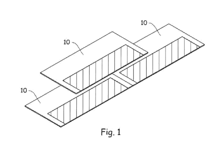
(0013] FIG,1 is a top perspective view of an illustrative group of
photovoltaic
devices as assembled.
[0014] FIG.2 is a top perspective view of a single photovoltaic device of FIG.
I
100151 FI .3 is a bottom perspective view of a single photovoltaic device of
I;1.
(00161 F K'3.4 is a top perspective view of a portion of single photovoltaic
device
with an exemplary pocket.
[0017] FIGS,5A-E are side views of exemplary pocket profile sections.
[0018] FIG.6 is a top perspective vies, of a single photovoltaic device with
an
ex -wip.lary liner strip,
[0019) FIG] is a side view of the exemplary liner strip of FIG.6 showing the
fold-
back
(0020] FlG.8 is a top perspective view of a single photovoltaic device with
another exemplary liner strip.
[0021] FIGa 9 is a top exploded perspective view of a single photovoltaic
device
and an exemplary end cap.
[00221 FIG, 10 is a top perspective asse mmhiy view of a single photovoltaic
device
and an exemplary end cap.
DETAILED DESCRIPTION OF THE PREFERRED EMBODIMENT
CA 02778494 2012-04-20
WO 2011/050225 PCT/US2010/053642
[0023] The present invention is directed to a photovoltaic assembly system for
securing and/or aligning at least a plurality of vertically adjacent
(overlapping)
photovoltaic device assemblies 10 (or overlapping photovoltaic device arrays)
to one
another, The devices 10 are preferably directly mounted to a structure (e.g.
building
structure, wall and/or roof deck) The present invention seeks to overcome the
issue
of wind uplift in with a unique interlocking solution and optionally taking
advantage of
that solution to address some of the other potential issues discussed above,
Fig, I
illustrate: r.hree photovoltaic devices 10 in an assembled arrangement (e.g. a
lower
photovoltaic device array cor sisti g of t vo horizontally adjacent devices
'10 and an
overlapping upper photovoltaic device array consisting of one device 10).
Photovoltaic Device
[0024] In general., the photovoltaic device 10 contempia ed by the present
invention is similar in construction to that disclosed in the PCT application
PCT./US09/42496 which claims priority to Provisional application 61/050,341;
both of which are incorporated by reference for all purposes, The device can
broadly
be described as an assembly of a multi-layered laminate (with polymeric and
non-
polymeric layers) which is encapsulated on at least three sides by a polymeric
casing. The device 10 is preferably adapted to mount directly to a structure,
such as
a building roof deck (with or without other items such as roofing felt or a
previous
layer of asphalt shingles), without the need for intermediate holding
structures (e. g,.
frames, rails, risers, or the like), In broad terms, the device 10 is intended
to be
installed on a building (e.g, roof) in a similar fashion as standard asphalt
shingles. In
a preferred embodiment, the device 10 is rectangular in shape, with a
generally flat
profile and with a thickness of io sa than about 20 mm, more preferably less
than
about 15mm and generally more than about 2 mm, more preferably more than about
5mm, It is contemplated that other shapes (srluare, round, polygon, etc..J),
other
profiles (e.g. curved, stepped, etc...), and thicknesses (greater than about
15mm) are
also possible.
[0025] p he photovoltaic device 10 may be further defined, as illustrated in
Figs. 2
and 3, as a device 10 with an active portion 20 and an inactive portion 40
immediately adjacent to and connected to the active ~: o i.sf?Ã 20.
[0026] The active portion 20 may include a photovoltaic cell assembly 22
having
a top surface portion 24 that allows transmission of light energy to a
photoective
portion 2 of the photovoltaic device 10 for conversion into el ctr Qal energy.
It also
has a bottom surface portion 28 having a bottom bonding zone 30.. It has a
peripheral edge 32 and a thickness 34.
6
CA 02778494 2012-04-20
WO 2011/050225 PCT/US2010/053642
[0027j The inactive portion 40 may include a region 42 for receiving a
fastener
(e,g, screw, nail, or other mechanical fasteners, not shown), the fastener
adapted to
connect the device 10 to a structure (e.g. a roof deck or wall). The inactive
portion
may also be defined as a top surface portion 44, a bottom surface portion 46
and a.
top bonding zone 48. It has a peripheral edge 50 and a thickness 52. The
inactive
portion 40 may also include a connection means, such as an electrical
connector
housing (not shown), that functions to string multiple devices 10 together.
[0028] The top bonding zone 48 and the bottom bonding zone, 30 may be further
defined to include a first bonding element 36 and the other comprises a second
bonding element 50, Functionally, the bonding elefn nts 36, 50 may be designed
to
interact with each other when the device 10 is vertically overlapped with an
adjacent
photovoltaic device tel. One of these bonding elements may also bond the
device 10
to the structure if there is no device immediately below it.
(002:9] Opiionally, the bonding zones 3, 48 may hc:itide apatteÃned surface
that
increases the surface area relative to a flat surface by more than 5%, more
preferably by more than 15%, and most preferably by more than 25%. It is
contemplated that there may also be the incorporation of structures (not
shown) that
have a vertical component (e,g. protrusions from the surfaces 28 and/or 44),
for
example to introduce a required shear component to the failure of the
adhesive. Also
contemplated is the addition of an open mesh structure or preventing a
tortuous
patch type of failure.
[0030] In one preferred embodiment, the top surface portion 44 of the
'inactive
portion is may include polyethylene, polypropylene, thermoplastic polyolefins
olefin
block copolymers, thermoplastic urethanes, silicones, and many other polymers
with
and without fillers, including particularly glass fillers,
[0031] In one preler redl embodiment, the bottom surface portion 28 of the
active
portion 20 may include thermoplastic polyolefin (TPO"), thermoplastic last am
r,
olefin block copolymers ("OBO"), natural rubbers, synthetic rubbers, polyvinyl
chloride, and other elastomeric and plasto eric materials, polyol fins,
polyester
amides, polysulfone, acetel, acrylic, polyvinyl chloride, nylon,
polycdrbonate,
phenolic, polyetheretherketone, polyethylene terephthalate, epoxies, including
glass
and mineral filled composites or any combination thereof:
Recessed Pocket(s)
[0032] It is contemplated that the device '10 may also include at least one
recessed pocket 60, see Figs 4. This pocket 60 may be disposed on the top or
bottom surface portions 28, 46 or on the top surfaces 24. 44 and generally has
a
depth less than the thicknesses 34, 52, In one preferred embodiment., the
pocket 60
7
CA 02778494 2012-04-20
WO 2011/050225 PCT/US2010/053642
has a pocket depth 62 of at least about 1. mrn. The pocket may span the device
(e.g, side to side) as a contiguous pocket or in segments of non-contiguous
pockets
(e.g, a plurality of pockets 60). The pocket(s) may be any number of shapes
ie_gg
square, rectangular, trapezoidal, circular, etc...) and have varied number of
pocket
profiles 84 (e g. concave, square, triangular, circular, or any combination
thereof), as
illustrated in Figs. 5A-E. Prefer h y, the poclkeii.: 50 have a geometric
shape and
profile adapted to accept either or boas bonding eiwments 36, 50.
Bonding Elements
[00331, Bonding elements .36, 50 generally function as the means for
connecting
(bonding) two at least partially vertically adjoining devices 10 to one.
another or in the
case of the "bottom" device 10, to the s:..UCtUra. It is contemplated that the
bonding
elements 36, 50 could be an adhesive, a hook and loop fastener assembly, or an
a.djoinsing surface (e.g. when an adhesive is only present on one side of the
joint
before assembly, the second element 50 is the adjoining surface).
Positionally, it is
preferred that at least one of the bonding elements be located at or near the
peripheral edge of one of the devices 10, although it is contemplated that the
bonding
elements could be nearer the center of the device 10. In one preferred
embodiment,
the first bonding element 36 is coextensive with or disposed within about 25
mm of
the peripheral edge of the active portion on the bottom surface portion 28 of
the
active portion 20. For clarification purposes, the terms "disposed" refers to
a location
of an element and 'connectively disposed" refers to the location and that the
elements are in contact with each other.
1OQ3$] In the case of an adhesive bonding element, it Is contemplated that the
adhesive chosen is at least partÃally~ :omp title with the surfaces being
bonded (e,g.
the polymeric surfaces of the devices 10 or the structure). In general, it is
preferred
that the bonding element comprises a adhesive that maintains a minimum peel
force
of about 3 PLI (pounds per linear inch.), more preferably about 5 PLI, and
most
preferred about 10 PLI or more, per ATM 0 903-98 at temperatures between n40"C
and 85vC and have an elongation of about >5O0%, more preferably> about 1000%
per ASTM 412-06, It is also preferred if the adhesive maintains a thickness
(after
assembly) of about O 5mm or more, more preferably from about 0.7mm to about
2.0mt.
[0035] In one preferred embodiment, the adhesive bondiin element is comprised
of a pressure sensitive adhesive (PSA) or a contact adhesive), that bonds to
surfaces
on contact (no curing time required) and to the respective surfaces (e.g.
adjoining
device 10. oz- structure or an asphalt shingle) with very slight pressure.
They may be
available in snly :nt and latex or water based forms. It is believed that
pressure
8
CA 02778494 2012-04-20
WO 2011/050225 PCT/US2010/053642
sensitive adhesives and x--tact adhesives are often based on non-cros lin ed
rubber adhesives,. acrylics or ipolyure hanes. It is also believed that
pressure
sensitive adhesives form visrcoelastic bonds that are aggressively and
permanently
tacky; adhere without the need of more than a finger or hand pressure; and
require
no activation by water, solvent or heat.
[00361 Pressure sensitive adhesives and contact adhesives may be available in
a
wide variety of chemical roompositions or systems. Some contemplated PSAs
include acrylic and metha rylate adhesives, rubber-based pressure sensitive
adhesives, styrene copolymers (SIS I SIBS), and sil`Ãcor es. Acrylic adhesives
are
known for excellent environmental resistance and fast-setl.ir time when:
compared
with other resin systems. Acrylic pressure sensitive adhesives often use an
acrylate
system. Ethylene ethyl acrylate (EEA) or ethyiene methyl acrylate (E A)
copolymers
are used to form hot melt PSA adhesives. Natural rubber, synthetic rubber or
elastamer sealants and adhesives can be based on a variety of systems such
silicone, polyurethane, chloroprene, butyl, polybutadiene, isoprene or
rn<eoprene. In a
preferred embodiment, the PSA include Ethylene Propylene Copolymer Tape,
rubber
based adhesives, synthetic rubber-based tape, PE foam tape, and acrylic based
and
or combination of the above in multi layer construction, e.g.,
Acry::ic/PET/Acrylic, The
most preferred adhesive being a butyl adhesive tape. It is contemplated that
some
important characteristics of the adhesive include adhesives with instant
aggressive
adhesion/tack to the roofing structure without the use of secondary materials
such as
primers, yet also has and retains high strength at and after weather extremes
(such
as elevated temperatures, e.g., 85'C, for prolonged periods, and provides
watertight
attachment of components to roofing structure, Some examples of commercially
available (and trademarked) adhesives may include: Butyl: Ashlan : F11joseal
Seam
tape, Adco PVA series (e ,g,, PVA 60O BT and 650BT); Rubber based. Adco SP-506
Cured Roofing Seam Tape; Synthetic rubber based: MA tao TM1039 and GS series;
Ethylene propylene copolymer: Sikai astomer68, AcryJli;c/PET/Acrylic:.: and
Tesa Tape
4965 PET reinforced; and PE Foam Tape; Tesa Tape 62932 DIC Foam Tape.
[00 371 In the case of a hook and loop fastener assembly, a minimum peel force
(between the hook and loop) of about 3 PLI (pounds per linear inch), more
preferably
about 5 Ell; and most preferred of about 10 PU or more per ASTM D 903-9 or
more at temperatures between -40"C and 85'C.. In this case, it is contemplated
that
the hook and loop fastener assembly is bonded to the device 10 (e.g. via
adhesive,
heat staked, over molded, ultrasonically welded, or mechanically fastened);
Removable Release Liner
9
CA 02778494 2012-04-20
WO 2011/050225 PCT/US2010/053642
OO38J In the case when an adhesive as discussed above is used, there may be
a need to include a removable release liner 80, illustrated in Figs. 6-8. It
is
contemplated that the removable release liner 80 may be used to aid n shipment
and
installation, as well as to ease the al`Ãgnment and placement of the two
devices 10 to
be bonded together. The liner 80 may also provide additional functi oi a y
discussed
as optional embodiments below=.
[00391 It is contemplated that the finer 80 may be constructed of relatively
thin
(e,g, less than about 1:Omm thick) essentially polymeric film. The liner 80
may be a
single layer film or may be a multi-layer film with multiple layers of the
same or
dissimilar materials. Some of the materials contemplated are, a high density
poly
ethylf ne (HDPE) and a poly-coated Kraft release paper (liner), It s believed
that
properties such as thickness and flexibility may be of some importance.
[0040] In one preferred embodiment, the removable release liner may be
disposed over the outer surfa;e of the adhesive and is removed to enaNe the
first
and second bonding eiemenis or the first bonding element. and the structure to
form a
bond
[00411 In another preferred embodiment, the removable release ner 80 extends
laterally from the periphery of the photovoltaic device by at least 10 mm
creating a
laterally extended portion 82. The liner 80 is also folded back upon itself at
least n
one of the bonding zones The fold making the paling off of the liner 80
easier.
(OO$2] in another preferred embodirrment, the removable release liner covers a
portion of the photoactive portion 26 and is not transparent (e,g opaque) or
light
limiting `e.g, at least for desired wavelengths or limiting enough to prevent
power
generation) to prevent the cell from generating electricity (e g. any
electricity or an
amount considered too high for safety of the system or an installer) until it
s
removed.
[0043] Optionally, the removable release liner may also include a print
installation
instruction (e.g. characters andk r pictographically information) for easy
access for
installer Doti{wally, the removable re oi,so finer may also inch de an outer
surface 84
with a slip protection (e,g, texture or high coefficient of friction).
Local Device Geometry
[00441 It is contemplated that may be desirous to increase the amount of
pressure applied at or near the front edge of the desire: '10, for example to
overcome
variations in device cant (e,g, in the installed position} as well as
variations n
mounting surface height,Jffatness. One way this may be accomplished by
shifting the
pressure point and force transmission in the device 10.
'
CA 02778494 2012-04-20
WO 2011/050225 PCT/US2010/053642
[00461 One possible way of shifting the pressure point and force transmission
may be to increase thickness of the device '10 at or ricer edge 92. This may
be
accomplished by local variation in the geometry of the device 10 (e.g, local
thickness
changes of about .5 to 1 mm),
(00461 This thickness increase may be provided by making the device thicker
by,
altering the shape of the mold or by separate component/components are added
(e.g. prior to or during installation) to the device I ct to locally increase
the height of
the device 10. It is contemplated that any number of components may serve this
purpose; for example, trim strips or clips that may be fastened to the device
10.
[0047] One illustrative example, where a single separate component (e<g. end
cap 90) is added, shown in rigs. 9 and 10. In this example the separate
component is a U-shaped channel that fits over one edge of the d ?vlca, The
end cap
90 is disposed over a top edge 92 of the device 10. It is contemplated that it
may be
desirous to fasten (e,g, nail) the device 10 as close to this location as
possible (, ..
within about 25mm or less) to set the height beneath the fastening region 42
in the
device 10,
Method
[0048] Also contemplated in the present invention is a method of assembling at
least two piiotovohtaic devices on a structure (the devices 10 as described
abov'e).
This inventive method may include the steps of, a. providing the at least two
photovoita;c devices, the devices including: a removable release liner, an
active
portion including n photovoltaic cell assembly having a top surface portion
that allows
transmission of light energy to the pt otoactlve portion for conversion into
electrical
err edgy and a bottom surface having a bottom bonding zone, and an inactive
portion
immediately adjacent to and connected to the active portion, the inactive
portion
having a region for receiving a fasterner to connect the device to the
structure nnd
having on a top surface a top bonding one; b. providing a plurality of
mechanical
fasteners; c. placing the one of the at least two photovoltaic d vices on the
structure;
d, securing the place: photovoltaic device to the structure with at least two
of the
plurality of mechanical fasteners, e, placing the second of the at least two
photovoltaic devices partially on the structure and partially on top of the
photovoltaic
device of step c; f, securing the second placed photovoltaic, device to the
structure
with at least two of the plurality of mechanical fasteners; and g. pressing
down on a
portion of the top surface portion of the second placed photovoltaic device,
completing the assembling of the at least two photovoltaic devices on the
structure,
[0049] Optionally, the method may also include: the at least two photovoltaic
devices include a removable release liner, wherein the release liner covers
the at
11
CA 02778494 2012-04-20
WO 2011/050225 PCT/US2010/053642
least one of the bonding zones, extends laterally from a periphery of the,
photovol`; ac
device by at least 10 mm creating a laterally extended portion, and is folded
back
upon itself at least in one of the bonding zones; the steps of removing the
removable
release liner by pulling on the laterally extended portion prior to the
pressing down
step; the removable release liner covers a portion of the top surface portion
of the
active portion and is non transparent or light limiting to prevent the cell
from
.generating electficity until it is removed; the removable release liner
includes a print
installation instruction for easy access for installer; the removable release
liner
includes an outer surface with a slip protection,
[OO5Oj Unless, state otherwise, dimensions and geometries of the various
structures depicted herein are. not intended to be restrictive of the
invention, and
other dimensions or geometries are possible. Plural structural components can
be
provided by a single integrated structure. Alternatively, a single integrated
structure
might be divided into separate plural components:. In addition, while a
feature of the
present invention may have been described in the context of only one of the
illustrated embodiments, such feature may be combined with one or more other
features of other embodiments, for any given application. It will also be
appreciated
from the above that the fabrication of the unique structures herein and the
Operation
thereof also constitute methods in accordance with the present invention.
[0051] The preferred embodiment of the present invention has been disclosed, A
person of ordinary skill in the art would realize however, that certain
modifications
would come within the teachings of this invention. Therefore, the following
claims
should be studied to determine the true scope and content of the invention.
(0052) Any numerical values recited in the above application include all
values
from the lower value to the upper value in increments of one unit provided
that there
is a separation of at least 2 units between any lower value and any higher
value. As
an example, if it is stated that the amount of a component or a value of a
process
variable such as, for example, temperature, pressure, time and the We is, for
example, from I to 90, preferably from 20 to 80, more preferably from 30 to
70, it is
intended that values such as 15 to 85, 22 to 68, 43 to 51, 30 to 32 etc. are
expressly
enumerated in this specification, For values which are less than one, one unit
i
considered to be 0,0001, 0001, 0.011 or 0.1 as appropriate. These are only
examples
of what is specifically intended and all possible combinst ons of numerical
values
between the lowest value and the highest value enumerated are to be considered
to
be expressly stated in this application in a similar manner.
(OQ53] Unless otheRvise stated, all ranges include both endpoints and all
cumbers between the endpoints. The use of "about" or "approximately" in
connection
12
CA 02778494 2012-04-20
WO 2011/050225 PCT/US2010/053642
with a range applies to both ends of the range, Thus, 'about 20 to 30" is
intended to
cover "out 20 to about 30", inclusive of at least the specified endpoints.
(0054] The disclosures of all articles and references, including patent
applications and publications, are incorporated by reference for all purposes.
[00-551 The term "consisting essentially of' to describe a combination shall
include the elements, ingredients, components or steps identified, and such
other
elements ingredients, components or steps that do not materially affect the
basic and
novel characteristics of the combination.
[p058] The use of the terms ":comprising" or "including" to describe
combinations
of elements, ingredients, comporienls or steps herein also contemplates
embodiments that consist essentially of the &ernents= ingredients, components
or
steps.
[0057 Plural elements, ingredients, components or steps can be provided by a
single integrated element, ingredienÃ, component or step, Alternatively, a
single
integrated element, ingredient, component or step might be divided into
separate
plural elements, ingredients, components or steps. The disclosure of "a. or
"one" to
describe an element, ingredient, component or step is not intended to
foreclose
additional elements, ingredients, components or steps. All references herein
to
elements or metals belonging to a certain Group refer to the Periodic Table of
the
Elements published and copyrighted by CRC Press, Inc., 1989. Any reference to
the
Group or Groups shall be to the Group or Groups as reflected in this Periodic
Table
of the Elements using the UPAC system for numbering groups,
13