Note: Descriptions are shown in the official language in which they were submitted.
CA 02779000 2012-04-25
WO 2011/051859 PCT/IB2010/054754
SELECTIVELY ACTIVATED RAPID START/BLEEDER CIRCUIT FOR
SOLID STATE LIGHTING SYSTEM
[0001] The present application relates to U.S. Provisional Application No.
60/247,297,
filed September 30, 2009, entitled "Rapid Start-Up Circuit for Solid State
Lighting System" and
incorporated herein by reference.
Technical Field
[0002] The present invention is directed generally to multi-tasking rapid
start-up circuits
for solid state lighting systems. More particularly, various inventive devices
and methods
disclosed herein relate to selectively providing a low impedance path of a
rapid start-up circuit
for use with a dimming circuit in a solid state lighting system at times other
than during a start-
up period.
Background
[0003] Solid state lighting technologies, i.e., illumination based on
semiconductor light
sources, such as light-emitting diodes (LEDs) and organic light-emitting
diodes (OLEDs), offer a
viable alternative to traditional fluorescent, high-intensity discharge (HID),
and incandescent
lamps. Functional advantages and benefits of LEDs include high energy
conversion and optical
efficiency, durability, lower operating costs, and many others. Recent
advances in LED
technology have provided efficient and robust full-spectrum lighting sources
that enable a variety
of lighting effects in many applications.
[0004] Some of the fixtures embodying these sources feature a lighting module,
including one or more LEDs capable of producing white light and/or different
colors of light,
e.g., red, green and blue, as well as a controller or processor for
independently controlling the
output of the LEDs in order to generate a variety of colors and color-changing
lighting effects,
for example, as discussed in detail in U.S. Patent Nos. 6,016,038 and
6,211,626, incorporated
herein by reference. LED technology includes line voltage powered white
lighting fixtures, such
as the EssentialWhiteTM series, available from Philips Color Kinetics.
[0005] Many lighting applications make use of dimmers. Conventional dimmers
work
well with incandescent (bulb and halogen) lamps. However, problems occur with
other types of
CA 02779000 2012-04-25
WO 2011/051859 PCT/IB2010/054754
-2-
electronic lamps, including compact fluorescent lamp (CFL), low voltage
halogen lamps using
electronic transformers and solid state lighting (SSL) lamps or units, such as
LEDs and OLEDs,
or other loads. Low voltage SSL units using electronic transformers, in
particular, may be
dimmed using special dimmers, such as, for example, electric low voltage (ELV)
type dimmers
or resistive-capacitive (RC) dimmers.
[0006] Conventional dimmers typically chop a portion of each waveform (sine
wave) of
the mains voltage signal and pass the remainder of the waveform to the
lighting fixture. A
leading edge or forward-phase dimmer chops the leading edge of the voltage
signal waveform.
A trailing edge or reverse-phase dimmer chops the trailing edge of the voltage
signal waveform.
Electronic loads, such as LED drivers, typically operate better with trailing
edge dimmers.
[0007] Unlike incandescent and other resistive lighting devices which respond
naturally
without error to a chopped waveform produced by a dimmer, LED and other SSL
units or
fixtures have a noticeable delay and/or flicker from when a user switches on
the light fixture to
when the light actually turns on. This delay from when the physical power
switch on the SSL
unit or fixture is turned on to when light is first seen from the fixture may
be undesirably long.
The cause of this delay is the time it takes for the power converter to have
enough voltage to start
up and begin converting power from the unrectified line voltage to power the
SSL unit or fixture
according to the dimmer setting. The time delay is determined by various
factors, such as the
available rectified voltage (Urect), e.g., as determined by the chopped
waveform of the mains
voltage signal based on dimmer setting, the impedance from the node Urect to
the node Vcc,
which supplies power to the power converter integrated circuit (IC), and the
capacitance from the
node Vcc to ground.
[0008] To address this delay, so-called "instant start" circuits have been
developed.
However, relatively low dimmer settings used in combination with instant start
circuits still
result in noticeable delay from the time the switch is flipped to turn on the
SSL unit or fixture to
the time light is seen. For example, an instant start circuit may be passive,
e.g., consisting of an
RC circuit. Generally, the lower the impedance of the start-up network, the
faster the power
converter will turn on. However, with the passive RC start-up network, steady
state power loss
increases with faster turn-on time, which results in lower power supply
efficiency and thus lower
overall fixture efficacy (e.g., lumens per watt).
CA 02779000 2012-04-25
WO 2011/051859 PCT/IB2010/054754
-3-
[0009] In addition, compatibility issues exist between dimmers and non-
resistive loads
following the start-up period, particularly due to low power of SSL loads.
Examples of
compatibility issues include misfiring of dimmer electronic switches,
providing supply voltage to
the power converter during low dimmer levels and discharging the system input
capacitors.
[0010] With respect to misfiring of dimmer electronic switches, in particular,
when the
dimmer electronic switch is closed (turned on), a voltage is applied to the
output of the dimmer,
and when the dimmer switch is open (turned off), no voltage is applied to the
output of the
dimmer. Different types of electronic switches may be used in conventional
dimmers. For
example, a TRIAC (TRIode Alternating Current) switch may be used, which
requires a
minimum holding current and/or latching current to stay turned on in order to
output the dimmer
voltage. However, low-wattage loads, such as LED lamps and other SSL units and
fixtures,
often fail to draw this minimum current. When the minimum current is not
drawn, the TRIAC
switches incorrectly (e.g., misfires), resulting in improper operation of the
dimmer/SSL unit or
fixture system. Such improper operation can result in undesirable effects,
such as flicker.
[0011] Thus, there is a need for an instant start circuit that that provides
sufficient power
to the power converter IC of a solid-state lighting unit or fixture over a
range of dim levels, and
particularly at comparatively low dim levels.
Summary
[0012] The present disclosure is directed to inventive methods and devices for
selectively implementing low impedance paths of a rapid start-up circuit of a
power converter for
solid state lighting units and fixtures, acting as a bleeder and improving
compatibility, during the
start-up period and during periods other than the start-up period, during
which the solid state
lighting units or fixtures are drawing insufficient current for proper
operation of the dimmer/SSL
system.
[0013] Generally, in one aspect, a device is provided to control current drawn
by a solid
state lighting (SSL) fixture, including a power converter and an SSL load. The
device includes a
rapid start/bleeder circuit having a selectable low impedance path, configured
to be temporarily
activated to form a low impedance connection between a voltage rectifier and
the power
converter providing power to the SSL load. The low impedance path is
temporarily activated
CA 02779000 2012-04-25
WO 2011/051859 PCT/IB2010/054754
-4-
during a start-up period to charge the power converter and during times other
than the start-up
period based on detected improper operation of the SSL fixture.
[0014] In another aspect, a system is provided for powering an SSL load, the
system
including a dimmer circuit, a rectifier circuit, a power converter, a rapid
start/bleeder circuit and
a controller. The dimmer circuit is configured to adjust a voltage of the SSL
load. The rectifier
circuit is configured to rectify the adjusted voltage output by the dimmer
circuit. The power
converter is configured to provide power to the SSL load based on the
rectified voltage output by
the rectifier circuit. The rapid start/bleeder circuit includes a low
impedance path, configured to
form a low impedance connection between the rectifier circuit and the power
converter when
activated. The controller is configured to selectively activate the low
impedance path of the
rapid start/bleeder circuit during a start-up period to charge the power
converter and during times
other than the start-up period based on current drawn by the SSL load.
[0015] In another aspect, a system is provided that includes a dimmer, a
rectifier, an
SSL fixture, a rapid start/bleeder circuit and a controller. The dimmer is
configured to adjust an
input voltage. The rectifier is configured to rectify the adjusted voltage
output by the dimmer
circuit. The SSL fixture includes a power converter and an SSL load, where the
power converter
provides power to the SSL load based on the rectified voltage output by the
rectifier. The rapid
start/bleeder circuit includes a low impedance path, configured to form a low
impedance
connection between the rectifier circuit and the power converter when
activated. The controller
is configured to monitor operation of the SSL fixture and to selectively
activate the low
impedance path of the rapid start/bleeder circuit during a start-up period to
charge the power
converter and during times other than the start-up period based on the
monitoring of the SSL
fixture operation.
[0016] As used herein for purposes of the present disclosure, the term "LED"
should be
understood to include any electroluminescent diode or other type of carrier
injection/junction-
based system that is capable of generating radiation in response to an
electric signal. Thus, the
term LED includes, but is not limited to, various semiconductor-based
structures that emit light
in response to current, light emitting polymers, organic light emitting diodes
(OLEDs),
electroluminescent strips, and the like. In particular, the term LED refers to
light emitting diodes
of all types (including semi-conductor and organic light emitting diodes) that
may be configured
CA 02779000 2012-04-25
WO 2011/051859 PCT/IB2010/054754
-5-
to generate radiation in one or more of the infrared spectrum, ultraviolet
spectrum, and various
portions of the visible spectrum (generally including radiation wavelengths
from approximately
400 nanometers to approximately 700 nanometers). Some examples of LEDs
include, but are
not limited to, various types of infrared LEDs, ultraviolet LEDs, red LEDs,
blue LEDs, green
LEDs, yellow LEDs, amber LEDs, orange LEDs, and white LEDs (discussed further
below). It
also should be appreciated that LEDs may be configured and/or controlled to
generate radiation
having various bandwidths (e.g., full widths at half maximum, or FWHM) for a
given spectrum
(e.g., narrow bandwidth, broad bandwidth), and a variety of dominant
wavelengths within a
given general color categorization.
[0017] For example, one implementation of an LED configured to generate
essentially
white light (e.g., LED white lighting fixture) may include a number of dies
which respectively
emit different spectra of electroluminescence that, in combination, mix to
form essentially white
light. In another implementation, an LED white light fixture may be associated
with a phosphor
material that converts electroluminescence having a first spectrum to a
different second
spectrum. In one example of this implementation, electroluminescence having a
relatively short
wavelength and narrow bandwidth spectrum "pumps" the phosphor material, which
in turn
radiates longer wavelength radiation having a somewhat broader spectrum. It
should also be
understood that the term LED does not limit the physical and/or electrical
package type of an
LED. For example, as discussed above, an LED may refer to a single light
emitting device
having multiple dies that are configured to respectively emit different
spectra of radiation (e.g.,
that may or may not be individually controllable). Also, an LED may be
associated with a
phosphor that is considered as an integral part of the LED (e.g., some types
of white light LEDs).
In general, the term LED may refer to packaged LEDs, non-packaged LEDs,
surface mount
LEDs, chip-on-board LEDs, T-package mount LEDs, radial package LEDs, power
package
LEDs, LEDs including some type of encasement and/or optical element (e.g., a
diffusing lens),
etc.
[0018] The term "light source" should be understood to refer to any one or
more of a
variety of radiation sources, including, but not limited to, LED-based sources
(including one or
more LEDs as defined above), incandescent sources (e.g., filament lamps,
halogen lamps),
fluorescent sources, phosphorescent sources, high-intensity discharge sources
(e.g., sodium
vapor, mercury vapor, and metal halide lamps), lasers, other types of
electroluminescent sources,
CA 02779000 2012-04-25
WO 2011/051859 PCT/IB2010/054754
-6-
pyro-luminescent sources (e.g., flames), candle-luminescent sources (e.g., gas
mantles, carbon
arc radiation sources), photo-luminescent sources (e.g., gaseous discharge
sources), cathode
luminescent sources using electronic satiation, galvano-luminescent sources,
crystallo-
luminescent sources, kine-luminescent sources, thermo-luminescent sources,
tribo luminescent
sources, sonoluminescent sources, radioluminescent sources, and luminescent
polymers.
[0019] The term "lighting fixture" is used herein to refer to an
implementation or
arrangement of one or more lighting units in a particular form factor,
assembly, or package. The
term "lighting unit" is used herein to refer to an apparatus including one or
more light sources of
same or different types. A given lighting unit may have any one of a variety
of mounting
arrangements for the light source(s), enclosure/housing arrangements and
shapes, and/or
electrical and mechanical connection configurations. Additionally, a given
lighting unit
optionally may be associated with (e.g., include, be coupled to and/or
packaged together with)
various other components (e.g., control circuitry) relating to the operation
of the light source(s).
An "LED-based lighting unit" refers to a lighting unit that includes one or
more LED-based light
sources as discussed above, alone or in combination with other non LED-based
light sources. A
"multi-channel" lighting unit refers to an LED-based or non LED-based lighting
unit that
includes at least two light sources configured to respectively generate
different spectrums of
radiation, wherein each different source spectrum may be referred to as a
"channel" of the multi-
channel lighting unit.
[0020] In one network implementation, one or more devices coupled to a network
may
serve as a controller for one or more other devices coupled to the network
(e.g., in a master/slave
relationship). In another implementation, a networked environment may include
one or more
dedicated controllers that are configured to control one or more of the
devices coupled to the
network. Generally, multiple devices coupled to the network each may have
access to data that
is present on the communications medium or media;, however, a given device may
be
"addressable" in that it is configured to selectively exchange data with
(i.e., receive data from
and/or transmit data to) the network, based, for example, on one or more
particular identifiers
(e.g., "addresses") assigned to it.
[0021] The term "controller" is used herein generally to describe various
apparatus
relating to the operation of one or more light sources. A controller can be
implemented in
CA 02779000 2012-04-25
WO 2011/051859 PCT/IB2010/054754
-7-
numerous ways (e.g., such as with dedicated hardware) to perform various
functions discussed
herein. A "processor" is one example of a controller which employs one or more
microprocessors that may be programmed using software (e.g., microcode) to
perform various
functions discussed herein. A controller may be implemented with or without
employing a
processor, and also may be implemented as a combination of dedicated hardware
to perform
some functions and a processor (e.g., one or more programmed microprocessors
and associated
circuitry) to perform other functions. Examples of controller components that
may be employed
in various embodiments of the present disclosure include, but are not limited
to, conventional
microprocessors, application specific integrated circuits (ASICs), and field-
programmable gate
arrays (FPGAs).
[0022] In various implementations, a processor and/or controller may be
associated with
one or more storage media (generically referred to herein as "memory," e.g.,
volatile and non-
volatile computer memory such as random-access memory (RAM), read-only memory
(ROM),
programmable read-only memory (PROM), electrically programmable read-only
memory
(EPROM), electrically erasable and programmable read only memory (EEPROM),
universal
serial bus (USB) drive, floppy disks, compact disks, optical disks, magnetic
tape, etc.). In some
implementations, the storage media may be encoded with one or more programs
that, when
executed on one or more processors and/or controllers, perform at least some
of the functions
discussed herein. Various storage media may be fixed within a processor or
controller or may be
transportable, such that the one or more programs stored thereon can be loaded
into a processor
or controller so as to implement various aspects of the present invention
discussed herein. The
terms "program" or "computer program" are used herein in a generic sense to
refer to any type of
computer code (e.g., software or microcode) that can be employed to program
one or more
processors or controllers.
[0023] The term "network" as used herein refers to any interconnection of two
or more
devices (including controllers or processors) that facilitates the transport
of information (e.g. for
device control, data storage, data exchange, etc.) between any two or more
devices and/or among
multiple devices coupled to the network. As should be readily appreciated,
various
implementations of networks suitable for interconnecting multiple devices may
include any of a
variety of network topologies and employ any of a variety of communication
protocols.
Additionally, in various networks according to the present disclosure, any one
connection
CA 02779000 2012-04-25
WO 2011/051859 PCT/IB2010/054754
-8-
between two devices may represent a dedicated connection between the two
systems, or
alternatively a non-dedicated connection. In addition to carrying information
intended for the
two devices, such a non-dedicated connection may carry information not
necessarily intended for
either of the two devices (e.g., an open network connection). Furthermore, it
should be readily
appreciated that various networks of devices as discussed herein may employ
one or more
wireless, wire/cable, and/or fiber optic links to facilitate information
transport throughout the
network.
[0024] It should be appreciated that all combinations of the foregoing
concepts and
additional concepts discussed in greater detail below (provided such concepts
are not mutually
inconsistent) are contemplated as being part of the inventive subject matter
disclosed herein. In
particular, all combinations of claimed subject matter appearing at the end of
this disclosure are
contemplated as being part of the inventive subject matter disclosed herein.
It should also be
appreciated that terminology explicitly employed herein that also may appear
in any disclosure
incorporated by reference should be accorded a meaning most consistent with
the particular
concepts disclosed herein.
Brief Description of the Drawings
[0025] In the drawings, like reference characters generally refer to the same
or similar
parts throughout the different views. Also, the drawings are not necessarily
to scale, emphasis
instead generally being placed upon illustrating the principles of the
invention.
[0026] FIG. 1 is a block diagram showing a rapid start circuit, according to a
representative embodiment.
[0027] FIG. 2 is a block diagram showing a rapid start circuit, according to a
representative embodiment.
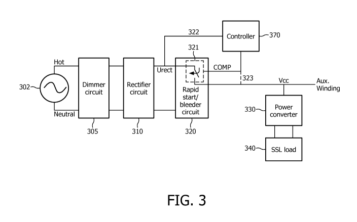
[0028] FIG. 3 is a block diagram showing a rapid start circuit multitasking as
a bleeder
circuit, according to a second representative embodiment.
[0029] FIGs. 4A and 4B show chopped, rectified voltage waveforms output by a
dimmer connected to a low power solid state lighting unit or fixture.
CA 02779000 2012-04-25
WO 2011/051859 PCT/IB2010/054754
-9-
[0030] FIG. 5 is a block diagram showing a rapid start circuit multitasking as
a bleeder
circuit, according to a representative embodiment.
[0031] FIG. 6 is a block diagram showing a rapid start circuit multitasking as
a bleeder
circuit, according to a representative embodiment.
[0032] FIG. 7 is a flow diagram showing a process of implementing a low
impedance
path of a rapid start circuit as a bleeder circuit, according to a
representative embodiment.
[0033] FIG. 8 is a block diagram showing a controller of a rapid start circuit
multitasking as a bleeder circuit, according to a representative embodiment.
Detailed Description
[0034] In the following detailed description, for purposes of explanation and
not
limitation, representative embodiments disclosing specific details are set
forth in order to provide
a thorough understanding of the present teachings. However, it will be
apparent to one having
ordinary skill in the art having had the benefit of the present disclosure
that other embodiments
according to the present teachings that depart from the specific details
disclosed herein remain
within the scope of the appended claims. Moreover, descriptions of well-known
apparatuses and
methods may be omitted so as to not obscure the description of the
representative embodiments.
Such methods and apparatuses are clearly within the scope of the present
teachings.
[0035] Applicants have recognized and appreciated that it would be beneficial
to
provide a circuit capable of reducing the delay between activating a switch of
a solid state
lighting unit or fixture and the turn-on time, particularly at low dimmer
settings. In other words,
to provide rapid start capability of a power converter for solid state
lighting units and fixtures at
low dimmer settings. Applicants have further recognized and appreciated that
it would be
beneficial to use the circuit capable of reducing the delay between activating
the switch and the
turn-on time also as a bleeder circuit, which is selectively activated to
provide a low impedance
path, as needed, to enable proper operation of the dimmer/SSL system,
including the solid state
lighting units and fixtures, at times other than start-up, as well as during
start-up.
[0036] FIG. 1 is a block diagram showing a rapid start circuit for powering a
solid state
lighting system, which can be multitasked as a selectively activated bleeder
circuit, according to
CA 02779000 2012-04-25
WO 2011/051859 PCT/IB2010/054754
-10-
various embodiments of the invention. Referring to FIG. 1, rapid start circuit
120 includes first
(depletion) transistor 127, second transistor 128, representative resistors
121-125 and diode 129
(shown separately). For purposes of the following explanation, the first
transistor 127 is a field-
effect transistor (FET) and the second transistor is a bipolar junction
transistor (BJT), although
other types of transistors may be implemented without departing from the scope
of the present
teachings. The rapid start circuit 120 provides voltage Vcc to power converter
130 (or power
converter IC) so that the power converter 130 can start up more quickly during
a start-up period,
and begin delivering power from the mains to the SSL load 140.
[0037] The start-up period is the time it takes for auxiliary winding 160 to
be fully
charged and for the voltage Vcc to reach a steady state value. The auxiliary
winding 160
provides voltage to Vcc node N102 when the power converter 130 is in steady
state operation.
However, the auxiliary winding 160 cannot be used to start up the power
converter 130 when the
power converter 130 is in the off state, so some other means, such as the
rapid start circuit 120, is
provided. The auxiliary winding 160 is typically taken as an extra winding off
of the main
power magnetic which the power converter 130 uses to convert power. The
auxiliary winding
160 therefore uses a small fraction of the energy in the main winding to power
the power
converter 130. The SSL load 140 may be part of a solid state lighting unit or
fixture (e.g.,
including the power converter 130) or other system, for example.
[0038] The rapid start circuit 120 receives (dimmed) rectified voltage Urect
through
diode bridge or bridge rectifier 110 from the dimmer (not shown) via Dim Hot
and Dim Neutral.
When a dimming setting has been selected, the rectified voltage Urect has
leading edge or
trailing edge chopped waveforms, the extent of which is determined by the
selected extent of
dimming, where low dimmer settings result in more significant waveform
chopping and thus a
lower RMS rectified voltage Urect. A rectified voltage Urect node N101 may be
coupled to
ground voltage through capacitor C111 (e.g., about 0.1 F) in order to filter
the switching current
of the power converter IC. Notably, the various values provided throughout the
description are
illustrative, and may be determined depending on the particular situation or
application specific
design requirements of various implementations, such as use of U.S. voltages,
E.U. voltages, or
some other voltages, as would be apparent to one skilled in the art.
CA 02779000 2012-04-25
WO 2011/051859 PCT/IB2010/054754
-11-
[0039] The rectified voltage Urect is connected through bridge rectifier 110
to a dimmer
(not shown) via lines DIM hot and DIM neutral. The dimmer initially receives
(undimmed)
unrectified voltage from the power mains. Generally, the unrectified voltage
is an AC line
voltage signal having a voltage value, e.g., between about 90VAC and about
277VAC, and
corresponding substantially sinusoidal waveforms. The dimmer includes an
adjuster, which
enables a dimming setting to be variably selected, e.g., manually by a user or
automatically by a
processor or other setting selection system. In an embodiment, the adjuster
enables settings
ranging from about 20 to 90 percent of the maximum light level of the SSL load
140. Also, in
various embodiments, the dimmer is a phase chopping (or phase cutting) dimmer,
which chops
either the leading edges or trailing edges of the input voltage waveforms,
thereby reducing the
amount of power reaching the SSL load 140. For purposes of explanation, it is
assumed the
dimmer is a trailing edge dimmer, which cuts a variable amount of the trailing
edges of the
unrectified sinusoidal waveforms.
[0040] Generally, the rapid start circuit 120 temporarily creates a low
impedance path
from Urect node N101 to Vcc node N102 during the start-up period, which occurs
when the
auxiliary winding 160 is not yet fully charged (for powering the power
converter 130) and the
voltage Vcc has not yet reached a steady state value. For example, when the
SSL load 140 is
turned-on (e.g., via the dimmer adjuster or other physical switch), the
initial voltage of the
auxiliary winding 160 is zero, and will remain zero until the power converter
130 has a chance to
start up during the start-up period. Power for start-up of the power converter
130 is drawn
through R121 (e.g., about 22k12) and the depletion first transistor 127 of the
rapid start circuit
120 to charge capacitors C112 and C 113. After the power converter 130 has
started up, the
auxiliary winding 160 provides the voltage Vcc to the power converter 130
through diode 150
and the first transistor 127 is made high impedance through activation of the
second transistor
128, as discussed a below. The capacitor C112 provides a small bypass
capacitance (e.g., about
0.1 F) connected between Vcc node N102 and ground in order to shunt high
frequency noise,
and the capacitor C113 provides a large bulk capacitance (e.g., about 10 F)
connected between
Vcc node N102 and ground, in order to provide lower frequency filtering and
temporary hold up.
[0041] More particularly, at the beginning of the start-up period, a COMP
signal
received at the base of the second transistor 128 is initially low. In the
depicted representative
embodiment, the second transistor 128 also includes a collector connected to
resistor R123 (e.g.,
CA 02779000 2012-04-25
WO 2011/051859 PCT/IB2010/054754
-12-
about 100k12) and an emitter connected to ground voltage. The low COMP signal
turns off the
second transistor 128, and thus the second transistor 128 is effectively open
circuited. In the
depicted embodiment, the COMP signal is provided through node N103, which is
connected to
voltage Vcc at Vcc node N102 through resistor R124 (e.g., about 100k12) and to
the ground
voltage through resistor 125 (e.g., about 100kS2). The COMP signal is
initially low because the
voltage Vcc is low, since the rectified voltage Urect has not charged the
auxiliary winding 160,
and thus the voltage Vcc at Vcc node N102 is not yet at the steady state
value. Because the
second transistor 128 is turned off, the gate of the depletion first
transistor 127 is connected to
the source of the depletion first transistor 127, for example, through
resistor R122 (e.g., about
100k12). In this state, the impedance of the depletion first transistor 127 is
low. A drain of the
first transistor 127 is connected to Urect node N101 through resistor R121
(e.g., about 22k12).
[0042] When the system is powered up, the rectified voltage Urect is high, and
the
voltage Vcc begins to charge through the resistor R121 and the first
transistor 127. When the
voltage Vcc is charged to the necessary voltage, the power converter 130
activates to power the
SSL load 140, and the COMP signal is brought high. The high COMP signal turns
on the second
transistor 128, which connects the gate of the first transistor 127 to ground
voltage through the
resistor R123. In this state, the first transistor 127 is turned off, and its
impedance becomes high,
which effectively disconnects the rectified voltage Urect at Urect node N101
from the Vcc node
N102. In other words, when the COMP signal is low, the rectified voltage Urect
at Urect node
N101 is connected to the Vcc node N202 through a low impedance, and when the
COMP signal
high, this low impedance is disconnected.
[0043] In addition, the rapid start circuit 120 includes the diode 129, which
separates the
large bulk capacitor C113 from the small bypass capacitor C 112, thereby
reducing the total
capacitance from Vcc node N102 to ground during the start-up transient. In an
embodiment, the
diode 129 includes an anode connected to ground through the capacitor C113 and
a cathode
connected to ground through the capacitor C112.
[0044] When the mechanical switch on the dimmer (not shown) is turned on, the
voltage
from the auxiliary winding 160 is at or near ground voltage, assuming the SSL
load 140 has been
off for a sufficiently long time, and the diode 129 is reverse biased. Because
the COMP signal is
initially low, the second transistor 128 is turned off, and the gate and
source of the first transistor
CA 02779000 2012-04-25
WO 2011/051859 PCT/IB2010/054754
- 13-
127 are connected, current is allowed to flow from rectified voltage Urect
node N201 through the
resistor R121 and the first transistor 127 to Vcc node N102, as discussed
above, initially
charging only the capacitor C112 and not the capacitor C113, which has been
effectively
removed from the circuit by the diode 129. Because the capacitor C112 is a
small value
capacitor used for bypassing Vcc node N202, the rapid start circuit 120 is
able to charge the
capacitor C112 to the operating voltage of the power converter 130 quickly,
even when the
rectified voltage Urect at Urect node N101 is very small, e.g., when the
dimmer is at its lowest
setting.
[0045] The large bulk capacitor C113 is not removed when Vcc is at the steady
state
voltage value, but only during the start-up period when the voltage at the
auxiliary winding 160
is low. That is, in steady state, the diode 129 conducts, enabling capacitor
C113 to be connected
to the voltage Vcc at Vcc node N102, providing the ripple reducing benefits of
a large bulk
capacitor. In addition, once the power converter 130 has started running, the
COMP signal goes
high and the second transistor 128 is switched on, causing the first
transistor 127 to turn off and
thus effectively disconnecting the rectified voltage Urect at Urect node N101
from the Vcc node
N 102, as discussed above.
[0046] Accordingly, the diode 129 of the rapid start circuit 120 effectively
switches out
the large bulk capacitance of the capacitor C113 during the start up
transient, but allows it to be
connected during steady state operation. By disconnecting the capacitor Cl 13
during start-up,
the voltage Vcc can be charged up faster, enabling rapid start even when the
rectified voltage
Urect is very low, such as when a dimmer is at its lowest setting.
[0047] In various embodiments, the dimmer may be a two- or three-wire
electronic low-
voltage (ELV) dimmer, for example, such as Lutron Diva DVELV-300 dimmer,
available from
Lutron Electronics Co., Inc. The SSL load 140 may be an LED or OLED lighting
unit or
lighting system, for example. The various components shown in FIG. 1 may be
arranged in
different pre-packaged configurations that may differ from the depicted
grouping. For example,
the bridge rectifier 110, the rapid start circuit 120, the power converter 130
and the SSL load 140
may be packaged together in one product, such as EssentialWhiteTM, lighting
fixture, available
from Philips Color Kinetics. Various embodiments may include any type of the
dimmer, lighting
system and/or packaging, without departing from the scope of the present
teachings.
CA 02779000 2012-04-25
WO 2011/051859 PCT/IB2010/054754
-14-
[0048] The dimmer provides the dimmed rectified voltage (e.g., having chopped
waveforms) to the power converter 130 though the bridge rectifier 100 and the
rapid start circuit
120. The power converter 130 may include structure and functionality
described, for example, in
U.S. Patent No. 7,256,554, to Lys, issued August 14, 2007, the subject matter
of which is hereby
incorporated by reference.
[0049] The power converter 130 may be constructed of any combination of
hardware,
firmware or software architectures, without departing from the scope of the
present teachings.
For example, in various embodiments, the power converter 130 may implemented
as a controller,
such as a microprocessor, ASIC, FPGA, and/or micro controller, such as an
L6562 PFC
controller, available from ST Microelectronics.
[0050] As stated above, when the dimmer is adjusted to a low setting,
resulting in an
RMS voltage of the dimmer output being fairly low (e.g., about 35V or less),
there would
typically not be enough energy transferred to the power magnetic for the
auxiliary winding 160
to power the power converter 130, resulting in shut down. However, in
accordance with the
present embodiment, the low dimmer level is detected by the failing of voltage
Vcc via the
divider formed by the resistors R124 and R125, and the rapid start circuit 120
is activated via the
COMP signal. Once the rapid start circuit 120 is activated, the power
converter 130 is supplied
from the rectified mains through the resistor R121 and the depletion first
transistor 127 (e.g.,
implemented as a FET). When the first transistor 127 is switched in, the power
converter 130 is
able to run even during low dimmer levels, preventing negative start-up
effects, such as delay
and flickering. In other embodiments, the low dimmer level may be detected by
an entity not
depicted in FIG. 1, such as a controller or micro controller, and the COMP
signal may be
controlled by this entity to activate or deactivate the rapid start circuit
120, as needed.
[0051] It is understood that, although representative values have been
provided above
for purposes of discussion, the values of the capacitors C111-C113 and the
resistors R121-R125
are determined depending on the particular situation or application specific
design requirements
of various implementations, as would be apparent to one skilled in the art.
[0052] FIG. 2 is a block diagram showing a rapid start circuit for powering a
solid state
lighting system, which can be multitasked as a selectively activated bleeder
circuit, according to
another representative embodiment. Referring to FIG. 2, rapid start circuit
220 includes
CA 02779000 2012-04-25
WO 2011/051859 PCT/IB2010/054754
- 15-
transistor 225, first diode 226, representative resistors 211-212 and second
diode 227 (shown
separately). For purposes of the following explanation, the transistor 225 is
a BJT and the first
diode is a zener diode, although other types of transistors and/or diodes may
be implemented
without departing from the scope of the present teachings. As discussed above
with respect to
the rapid start circuit 120 in FIG. 1, the rapid start circuit 220 provides
voltage Vcc to power
converter 230 (or power converter IC) for powering SSL load 240 during a start-
up period, until
auxiliary winding 260 is fully charged and the voltage Vcc has a steady state
value.
[0053] The rapid start circuit 220 receives (dimmed) rectified voltage Urect
through
diode bridge or bridge rectifier 210 from the dimmer via Dim Hot and Dim
Neutral. When a
dimming setting has been selected, the rectified voltage Urect has leading
edge or trailing edge
chopped waveforms, the extent of which is determined by the selected dimming
setting, where
low dimmer settings result in more significant waveform chopping and thus a
lower RMS
rectified voltage Urect. A rectified voltage Urect node N201 may be coupled to
ground voltage
through capacitor C211 (e.g., about 0.1 F) in order to filter the switching
current of the power
converter.
[0054] The rectified voltage Urect is provided through the bridge rectifier
210 from a
dimmer (not shown) via lines DIM hot and DIM neutral. The dimmer initially
receives
(undimmed) unrectified voltage from a power source via the power mains.
Generally, the
unrectified voltage is an AC line voltage signal having a voltage value, e.g.,
between about
90VAC and about 277VAC, and corresponding substantially sinusoidal waveforms.
The
dimmer includes an adjuster, which enables a dimming setting to be variably
selected, e.g.,
manually by a user or automatically by a processor or other setting selection
system. In an
embodiment, the adjuster enables settings ranging from about 20 to 90 percent
of the maximum
light level of the SSL load 240, for example. Also, in various embodiments,
the dimmer is a
phase chopping (or phase cutting) dimmer, which chops either the leading edges
or trailing edges
of the input voltage waveforms, thereby reducing the amount of power reaching
the SSL load
240.
[0055] The rapid start circuit 220 is particularly effective at very low
dimming settings.
According to the depicted representative embodiment, even when the rectified
voltage Urect at
Urect node N201 is very low (e.g., at the lowest dimmer setting), the rapid
start circuit 220
CA 02779000 2012-04-25
WO 2011/051859 PCT/IB2010/054754
-16-
avoids visible delay by lowering the capacitance from the voltage Vcc at Vcc
node N202 to
ground voltage during the start-up period, in addition to lowering resistance
from the rectified
voltage Urect at Urect node N201 to the voltage Vcc at Vcc node N202 during
the start-up
period. After the power converter 230 has started up, the auxiliary winding
260 provides the
voltage Vcc to the power converter 230 through second diode 227 and third
diode 250, discussed
below.
[0056] More particularly, the rapid start circuit 220 shown in FIG. 2 includes
the first
diode 226 having a cathode connected to node N203 and an anode connected to a
ground
voltage. The rapid start circuit 220 also includes the transistor 225, having
a base connected to
node N203, a collector connected to Urect node N201 (rectified voltage Urect)
through resistor
R212 (e.g., about 5kS2), and an emitter connected to Vcc node N202 (voltage
Vcc). Node N203
is also connected to Urect node N201 through resistor R211 (e.g., about
200k12). The resistor
8211 enables enough current to flow through the first diode 226 to keep the
base of the transistor
225 slightly below the steady state voltage value of Vcc at Vcc node N202 when
the voltage Vcc
has been fully charged. However, when the voltage Vcc is below the voltage at
the base of the
transistor 225, such as during start up, the transistor 225 turns on,
providing a low impedance
path from the rectified voltage Urect to the voltage Vcc through the resistor
R212 and the
transistor 225, thus lowering the impedance from the rectified voltage node
Urect N201 to the
Vcc node N202 during the start-up transient, prior to the charging of the
auxiliary winding 260.
[0057] In addition, rapid start circuit 220 includes the second diode 227,
which separates
the large bulk capacitance, capacitor C213 (e.g., about 10 F), from the small
bypass capacitance,
capacitor C212 (e.g., about 0.1 F), thereby reducing the total capacitance
from Vcc node N202
to ground during the start-up transient. In an embodiment, the second diode
227 includes an
anode connected to ground through the capacitor C213 and a cathode connected
to ground
through the capacitor C212.
[0058] When the mechanical switch on the dimmer (not shown) is turned on, the
voltage
from the auxiliary winding 260 is at or near ground voltage, assuming the SSL
load 240 has been
off for a sufficiently long time, and the second diode 227 is reverse biased.
Because the resistor
8211 biases the first diode 226, the transistor 225 turns on, allowing current
to flow from
rectified voltage Urect node N201 through the resistor R212 and the transistor
225 to Vcc node
CA 02779000 2012-04-25
WO 2011/051859 PCT/IB2010/054754
-17-
N202, as discussed above, initially charging only the capacitor C212 and not
the capacitor C213,
which has been effectively removed from the circuit by the second diode 227.
Because the
capacitor C212 is a small value capacitor used for bypassing Vcc node N202,
the rapid start
circuit 220 is able to charge the capacitor C212 to the operating voltage of
the power converter
230 quickly, even when the rectified voltage Urect at Urect node N201 is very
small, e.g., when
the dimmer is at its lowest setting.
[0059] The large bulk capacitor C213 is not removed when Vcc is at the steady
state
voltage value, but only during the start-up period when the voltage at the
auxiliary winding 260
is low. That is, in steady state, second diode 227 conducts, enabling the
capacitor C213 to be
connected to the voltage Vcc at Vcc node N202, providing the ripple reducing
benefits of a large
bulk capacitor. In addition, once the power converter 230 has started running,
the transistor 225
is switched off because the first diode 226 is chosen to have a breakdown
voltage slightly below
the steady state voltage Vcc. In this manner, the second diode 227 effectively
switches out the
large bulk capacitance of the capacitor C213 during the start up transient,
but allows it to be
connected during steady state operation. By disconnecting the capacitor C213
during start-up,
the voltage Vcc can be charged up faster, enabling rapid start even when the
rectified voltage
Urect is very low, such as when a dimmer is at its lowest setting.
[0060] It is understood that, although some representative values have been
provided
above for purposes of discussion, the values of the capacitors C211-C213 and
the resistors R211-
R212 are determined depending on the particular situation or application
specific design
requirements of various implementations, as would be apparent to one skilled
in the art.
[0061] In the representative rapid start-up circuits described above with
reference to
FIGs. 1 and 2, a low impedance path is selectively provided to energize a
power converter IC
(e.g., power converter 130, 230) prior to the power converter IC energizing an
auxiliary winding
(e.g., auxiliary winding 160, 260) on the power magnetic to power itself. Once
the auxiliary
winding is energized and the power converter IC (and voltage Vcc) is in steady
state, the low
impedance path is removed, drawing no steady state power. Generally, the lower
the impedance
of the start up network, the faster the power converter IC will turn on.
However, during steady
state operation (e.g., after the start-up period), there are times that the
solid state lighting unit or
fixture draws insufficient current to sustain proper operation. Thus,
according to various
CA 02779000 2012-04-25
WO 2011/051859 PCT/IB2010/054754
- 18-
embodiments discussed below, the low impedance path of the rapid start-up
circuit is selectively
activated in response to this condition, multitasking the rapid start-up
circuit to also act as a
bleeder circuit.
[0062] FIG. 3 is a block diagram showing a rapid start circuit multitasking as
a bleeder
circuit, according to a representative embodiment. Referring to FIG. 3, dimmer
circuit 305
receives rectified voltage from power mains 302. The dimmer circuit 305
includes an adjuster
(not shown), which enables a dimming setting to be variably selected, e.g.,
manually by a user or
automatically by a processor or other setting selection system. In an
embodiment, the adjuster
enables settings ranging from about 20 to 90 percent of the maximum light
level of the SSL load
340. Also, in various embodiments, the dimmer circuit 305 is a phase chopping
(or phase
cutting) dimmer, which chops either the leading edges or trailing edges of the
input voltage
waveforms, thereby reducing the amount of power reaching the SSL load 340. The
rectifier
circuit 310 rectifies the dimmed voltage (Urect) to be provided to the power
converter 330
through the multitasking rapid start/bleeder circuit 320.
[0063] As described above, the rapid start/bleeder circuit 320 includes a
selectable low
impedance path 321. The selectable low impedance path 321 is indicated by a
switch for
convenience of explanation, where the low impedance path 321 is provided
(switched in) when
the switch is closed, and removed (switched out) when the switch is opened.
The rapid
start/bleeder circuit 320 and/or the low impedance path 321 may be implemented
in various
configurations without departing from the scope of the present teachings. For
example, referring
to FIGs. 1 and 2, the low impedance path 321 may include the resistor R121 and
the first
transistor 127 (in the on state) of the rapid start circuit 120 in FIG. 1, or
the resistor R212 and the
transistor 225 (in the on state) of the rapid start circuit 220 in FIG. 2.
Other examples of the
rapid start/bleeder circuit 320 and the low impedance path 321 are discussed
below with
reference to FIGs. 5 and 6.
[0064] In a representative embodiment, the low impedance path 321 is switched
in to
the circuit in response to a COMP signal. The COMP signal may be provided, for
example, by
controller 370. The controller 370 is configured to detect conditions in which
the current drawn
by the SSL load 340 is insufficiently low to enable proper operation of the
SSL load 340. This
condition may be indicated, for example, by the voltage level of voltage Vcc
at the power
CA 02779000 2012-04-25
WO 2011/051859 PCT/IB2010/054754
-19-
converter 330 or the voltage level of the dimmed rectified voltage Urect
output by the rectifier
circuit 310. For example, the controller 370 may measure the level of the
dimmed rectified
voltage Urect via control line 322. When the voltage level of the dimmed
rectified voltage Urect
is below a predetermined threshold, which may be determined depending on the
particular
situation or application specific design requirements of various
implementations, the controller
370 drives the COMP signal to a level enabling activation of the low impedance
path 321. At
other times, when the dimmed rectified voltage Urect is not below the
predetermined threshold,
the controller 370 drives the COMP signal to another level for deactivating
the low impedance
path 321. Alternatively, the controller 370 may measure current flow, e.g.,
through a current
detector (not shown) at the SSL load 340. When the current flow is below a
predetermined
threshold or stops altogether, the controller drives the COMP signal to the
level enabling
activation of the low impedance path 321. Of course, the controller 370 may be
configured to
activate the low impedance path 321 based on various other triggers without
departing from the
scope of the present teachings. For example, the controller 370 may measure
the on-time of the
electronic switch (e.g., TRIAC or FET) of the dimmer circuit 305, and activate
the low
impedance path 321 following a predetermined amount of on-time (e.g., about
2.5 ms).
[0065] In an alternative embodiment, the COMP signal is not provided by the
controller
370. Rather, the COMP signal may be generated by the rapid start/bleeder
circuit 320 itself, e.g.,
based on feedback from Vcc node via optional signal line 323. For example, the
rapid
start/bleeder circuit 320 may be configured substantially the same as the
representative rapid
start circuit 120 in FIG. 1. Referring to FIG. 1, further to the initial start-
up, the rectified voltage
Urect is high and the voltage Vcc is charged to the necessary voltage, so that
the power converter
130 powers the SSL load 140. Also, in this state, the COMP signal is high,
which turns on the
second transistor 128, connecting the gate of the first transistor 127 to
ground voltage through
the resistor R123, causing the first transistor 127 to turn off. Because the
first transistor 127 is
turned off, its impedance becomes high, which effectively disconnects the
rectified voltage Urect
at Urect node N101 from the Vcc node N102, e.g., effectively removing the low
impedance path
321 from the circuit.
[0066] However, when voltage Vcc drops below an operational threshold and/or
current
drawn by the LED load 140 and power converter 130 drops to an inadequate level
or stops
altogether, the second transistor 128 is turned off by the low signal received
at its base through
CA 02779000 2012-04-25
WO 2011/051859 PCT/IB2010/054754
-20-
the resistor R124, which is effectively the same as providing a low COMP
signal. Once the
second transistor 128 is turned off, the gate of the depletion first
transistor 127 is connected to its
source, for example, through resistor R122, creating a low impedance
connection between the
Urect node N101 and the Vcc node N102, e.g., effectively creating the low
impedance path 321.
[0067] The rapid start/bleeder circuit 320 enables proper operation of the SSL
load 340
to be maintained, even during periods of low voltage and/or insufficient
current draw, without
having to configure and control a separate bleeder circuit. Rather, the low
impedance path 321
used for rapid start-up is likewise used selectively after start-up to draw
current from the mains
302 to improve compatibility of the SSL load 340 and the dimmer circuit 305,
when needed.
That is, switching in the low impedance path 321, e.g., by turning on the
second transistor 128 of
FIG. 1, at appropriate times during all or part of the line cycle enables the
low impedance path
321 to be used as a low impedance bleeder. Thus, according to various
embodiments, no
additional bleeder circuit is needed to make the SSL load 340 more compatible
with dimmers.
This approach is suitable in any instance where a non-resistive load is
connected to a dimmer.
[0068] There are a number of potential incompatibilities between the dimmer
circuit 305
and the SSL load 340 that can be addressed by the selective activation of the
low impedance path
321. For example, TRIAC switches are widely used as dimmer switches,
particularly in
households, because they typically are the least expensive solution. However,
as discussed
above, a TRIAC switch requires minimum holding and latching currents to
correctly switch. For
example, a dimmer such as a Lutron D-600PH dimmer, available from Lutron
Electronics Co.,
Inc., may incorporate a BTA08-600BRG TRIAC, available from STMicroelectronics,
which has
a holding current and a latching current of about 50 mA. Thus, a minimum load
of several watts
(e.g., about 40 W) must be maintained for proper operation. As a result, such
dimmers typically
switch improperly (e.g., misfire) when used for low-wattage LED lamps and
other SSL units and
fixtures that provide small loads, particularly at lower dimmer settings. For
example, eW Profile
Powercore LED fixtures and eW Downlight Powercore LED fixtures, available from
Philips
Solid State Lighting Solutions, provide loads of only about 6 W and about 15
W, respectively.
Therefore, the minimum holding and latching currents may not be maintained by
the TRIAC
switch.
CA 02779000 2012-04-25
WO 2011/051859 PCT/IB2010/054754
-21-
[0069] However, according to various embodiments, misfiring of a TRIAC switch
can
be detected by measuring the output voltage of the dimmer circuit 305 during
operation, e.g., at
the Urect node. FIG. 4A shows an example of a TRIAC switch misfiring. In
particular, FIG. 4A
shows a chopped, rectified voltage waveform 410 output by the dimmer circuit
305 connected to
a low power SSL unit or fixture, such as SSL load 340. During each mains
voltage half-wave,
the TRIAC switch is fired multiple times. However, only once does this result
in proper turn-on,
indicated by the generally smooth sinusoidal curve at the trailing edge of the
waveform 410. In
the other attempts, the TRIAC switch snaps-off after almost immediately after
triggering, and
tries to turn on again a few milliseconds later. Visible flicker in the light
output by the SSL unit
or fixture results.
[0070] To prevent this condition, the low impedance path 321 of the
multitasking rapid
start/bleeder circuit 320 is selectably activated when current drawn by the
SSL load 340 drops
below a predetermined threshold. Thus, in the example of the TRIAC switch, the
low impedance
path 321 is temporarily created between the dimmer circuit 305 and the power
converter 330,
forcing the holding and latching currents of the TRIAC switch in the dimmer
circuit 305 to be
drawn and otherwise preventing the TRIAC switch from misfiring. FIG. 4B shows
a
representative chopped, rectified voltage waveform 411 output by the dimmer
circuit 305 after
creation of the low impedance path 321 of the rapid start/bleeder circuit 320.
[0071] Another example of potential incompatibility between the dimmer circuit
305
and the SSL load 340 occurs when the dimmer circuit 305 is set at low dimmer
levels, resulting
in a dimmed rectified voltage Urect too low for the power converter 330 to
operate. For
example, the output of the dimmer circuit 305 can be fairly low, e.g., about
35 V, and as a result,
there is not enough energy transferred to the power magnetic for the auxiliary
winding to power
the power converter 330, resulting in shut down. However, according to various
embodiments,
the low impedance path 321 is switched in to supply the power converter 330
when the dimmed
rectified voltage Urect is at too low of a voltage level. For example, the low
voltage level is
detected by the controller 370 and the low impedance path 321 is then switched
in to supply the
power converter 330 directly from the rectified mains of the rectifier circuit
310. Accordingly,
the power converter 330 can run even during time periods when low voltage
levels are output by
the dimmer circuit 305.
CA 02779000 2012-04-25
WO 2011/051859 PCT/IB2010/054754
-22-
[0072] Yet another example of incompatibility between the dimmer circuit 305
and the
SSL load 340 results from capacitance when an electronic switch (not shown) of
the dimmer
circuit 305 is open (i.e., the switch is off). That is, when the dimmer
electronic switch is open,
the mains voltage is present across a capacitive divider consisting of a
fixture input capacitor
(not shown), connected to the Dim Hot line (between the dimmer circuit 305 and
the rectifier
circuit 310) and ground voltage, and a dimmer electromagnetic interference
(EMI) capacitor (not
shown), connected in parallel with the dimmer switch. Because the fixture
input capacitor and
the EMI capacitor may be near the same order of magnitude, some voltage is
present across the
power converter 330 from the impedance divider formed by the two
aforementioned capacitors
even when the dimmer switch is open, causing unstable operation. However,
according to
various embodiments, by switching in the low impedance path 321, a low
impedance is created
in parallel with the fixture input capacitor, and thus the voltage seen by the
power converter 330
is reduced to an insignificant level.
[0073] FIGs. 5 and 6 are block diagrams showing rapid start circuits
multitasking as
bleeder circuits, according to representative embodiments. Referring to FIG.
5, rapid
start/bleeder circuit 520 includes first (depletion) transistor 527, second
transistor 528 and
representative resistors R521-R523. For purposes of the following explanation,
the first
transistor 527 is a FET and the second transistor 528 is a BJT, although other
types of transistors
may be implemented without departing from the scope of the present teachings.
The rapid
start/bleeder circuit 520 provides voltage Vcc to power converter 530 (or
power converter IC) to
start the power converter 530 more quickly during a start-up period to begin
delivering power
from the mains to the SSL load 540, and after the start-up period, to deliver
power from the
mains to the SSL load 540 when the SSL load 540 is otherwise drawing
insufficient current to
enable normal operation. Capacitors C511-C513 and diode 550 are substantially
the same as
capacitors C111-C113 and diode 150 of FIG. 1, and therefore the descriptions
will not be
repeated with respect to FIG. 5.
[0074] The rapid start/bleeder circuit 520 receives (dimmed) rectified voltage
Urect
through diode bridge or bridge rectifier 510 from the dimmer (not shown) via
Dim Hot and Dim
Neutral. When a dimming setting has been selected, the rectified voltage Urect
may have
leading edge or trailing edge chopped waveforms, the extent of which is
determined by the
selected extent of dimming, where low dimmer settings result in more
significant waveform
CA 02779000 2012-04-25
WO 2011/051859 PCT/IB2010/054754
-23-
chopping and thus a lower RMS rectified voltage Urect. A rectified voltage
Urect node N501
may be coupled to ground voltage through capacitor C511 in order to filter the
switching current
of the power converter 530.
[0075] After start-up and during normal operation of the SSL load 540 and/or
normal
voltage levels at Urect node N501, the COMP signal received at the base of the
second transistor
528 is at a first level (e.g., a high level), e.g., as provided by the
controller 370 (not shown in
FIG. 5). In the depicted representative embodiment, the second transistor 528
also includes a
collector connected to resistor R523 (e.g., about 100kS2). In response to the
high COMP signal
at its base, the second transistor 528 is turned on, connecting the gate of
the first transistor 527 to
ground voltage through the resistor R523. In this state, the first transistor
527 is turned off, and
its impedance becomes high, which effectively disconnects the rectified
voltage Urect at Urect
node N501 from the Vcc node N502, thus removing the low impedance path,
including the
resistor R521 (e.g., about 22k12) and the first transistor 527, from between
the Urect node N501
and the Vcc node N502.
[0076] However, due to the low power of the SSL load 540, the current drawn by
the
SSL load 540 may stop or otherwise drop below a predetermined level during
normal operation.
This condition may be detected, for example, by continually or periodically
measuring the
dimmed rectified voltage at Urect node N501 and comparing the measured voltage
to a
predetermined threshold value (e.g., using the controller 370), which
corresponds to the
inadequate current levels. In response, the COMP signal is set to a second
level (e.g., a low
level), e.g., as provided by the controller 370. In the depicted
representative embodiment, the
second transistor 528 is turned off in response to the low COMP signal,
disconnecting the gate of
the first transistor 527 from ground voltage and connecting the gate of the
first transistor 527 to
the source of the first transistor 527 through resistor R522 (e.g., about
100k12). In this state, the
impedance of the depletion first transistor 527 becomes low. A drain of the
first transistor 527 is
connected to Urect node N501 through resistor R521. Thus, a low impedance path
is created
between the Urect node N501 and the Vcc node N502, including the resistor R521
and the first
transistor 527. In other words, when the COMP signal is low, the rectified
voltage Urect at Urect
node N501 is connected to the Vcc node N202 through the low impedance path,
and when the
COMP signal high, the low impedance path is disconnected.
CA 02779000 2012-04-25
WO 2011/051859 PCT/IB2010/054754
-24-
[0077] Referring to FIG. 6, rapid start/bleeder circuit 620 includes first
transistor 625,
second transistor 628, first diode 626 (e.g., a zener diode) and
representative resistors R611-
R612. For purposes of the following explanation, the first and second
transistors 625 and 628
are BJTs, although other types of transistors may be implemented without
departing from the
scope of the present teachings. The rapid start/bleeder circuit 620 provides
voltage Vcc to power
converter 630 to start the power converter 630 more quickly during a start-up
period to begin
delivering power from the mains to the SSL load 640, and after the start-up
period, to deliver
power from the mains to the SSL load 640 when the SSL load 640 is otherwise
drawing
insufficient current to enable normal operation. Capacitors C611-C613 and
second diode 650 are
substantially the same as capacitors C211-C213 and diode 250 of FIG. 2, and
therefore the
descriptions will not be repeated with respect to FIG. 6. The rapid
start/bleeder circuit 620
receives (dimmed) rectified voltage Urect through diode bridge or bridge
rectifier 610 from the
dimmer (not shown) via Dim Hot and Dim Neutral, as discussed above.
[0078] The first diode 626 has a cathode connected to node N603 and an anode
connected to the second transistor 628. The first transistor 625 includes a
base also connected to
node N603, a collector connected to Urect node N601 (rectified voltage Urect)
through resistor
R612 (e.g., about 5kS2), and an emitter connected to Vcc node N602 (voltage
Vcc). Node N603
is also connected to Urect node N601 through resistor R611 (e.g., about
200k12). After start-up
and during normal operation of the SSL load 640 and/or normal voltage levels
at Urect node
N601, the COMP signal received at the base of the second transistor 628 is at
a first level (e.g., a
high level), e.g., as provided by the controller 370 (not shown in FIG. 6).
[0079] In the depicted representative embodiment, the second transistor 628
also
includes a collector connected to the anode of the first diode 626 and an
emitter connected to
ground voltage. In response to the high COMP signal at its base, the second
transistor 628 is
turned on, connecting the anode of the first diode 626 to ground voltage
enabling normal
operation. In this state, the resistor R611 enables enough current to flow
through the first diode
626 to keep the base of the transistor 625 slightly below the steady state
voltage value of Vcc at
Vcc node N602 when the voltage Vcc has been fully charged at start-up or when
the SSL load
640 is otherwise drawing sufficient current. The low impedance path, including
the resistor
R612 and the first transistor 625, is therefore not formed between the Urect
node N601 and the
Vcc node N602.
CA 02779000 2012-04-25
WO 2011/051859 PCT/IB2010/054754
-25-
[0080] However, when the voltage Vcc is below the voltage at the base of the
transistor
625, such as during start-up or when the SSL load 640 is not drawing
sufficient current, the first
transistor 625 turns on, providing a low impedance path from the rectified
voltage Urect to the
voltage Vcc through the resistor R612 and the transistor 625, thus lowering
the impedance from
the rectified voltage node Urect N601 to the Vcc node N602. In addition, this
condition is
detected, for example, by continually or periodically measuring the dimmed
rectified voltage at
Urect node N601 and comparing the measured voltage to a predetermined
threshold value (e.g.,
using the controller 370), which corresponds to the inadequate current levels.
Accordingly, the
COMP signal is set to a second level (e.g., a low level), which turns off the
second transistor
628, disconnecting the anode of the first diode 626 from ground voltage and
further causing 625
to turn on to provide the low impedance path from the rectified voltage Urect
to the voltage Vcc
through the resistor R612 and the transistor 625. Thus, in steady state, when
Vcc is fed from the
auxiliary winding, when the COMP signal is low, the rectified voltage Urect at
Urect node N601
is connected to the Vcc node N602 through the low impedance path, and when the
COMP signal
high, the low impedance path is disconnected. In other words, in the depicted
embodiment,
when the COMP signal is low, the bleeder is always activated.
[0081] FIG. 7 is a flow diagram showing a process of implementing a low
impedance
path of a rapid start circuit as a bleeder circuit, according to a
representative embodiment.
Referring to FIGs. 3 and 7, the controller 370 determines the threshold
voltage of the dimmed
rectified voltage Urect, which triggers activation of the low impedance path
321, in block 710.
The threshold voltage may be determined, for example, based on the type of
dimmer circuit 305
and/or the corresponding dimmer setting, the type of SSL load 340 and/or
corresponding power
requirements, or other factors indicating at what voltage the SSL load 340
will stop drawing
current or otherwise begin functioning incorrectly. The controller 370 may
access a previously
stored look-up table, for example, associating various dimmer circuits, dimmer
settings, SSL
loads, and the like, with corresponding threshold voltages. As discussed
above, triggers other
than the value of the dimmed rectified voltage Urect may be used to determine
when to activate
the low impedance path 321, without departing from the scope of the present
teachings.
[0082] In block 712, the controller 370 receives voltage measurements from the
rectifier
circuit 310, indicating the value of the dimmed rectified voltage Urect. The
controller 370
compares the measured voltage to the threshold voltage in block 714. When the
measured
CA 02779000 2012-04-25
WO 2011/051859 PCT/IB2010/054754
-26-
voltage is not below the threshold voltage (block 714: No), indicating that
the power converter
330 and the SSL load 340 are functioning properly, the controller 370 outputs
the COMP signal
having a first (e.g., high) level in order to deactivate the low impedance
path 321. When the
measured voltage is below the threshold voltage (block 714: Yes), indicating
that the power
converter 330 and/or the SSL load 340 are not functioning properly, the
controller 370 outputs
the COMP signal having a second (e.g., low) level in order to activate the low
impedance path
321, causing the rapid start/bleeder circuit 320 to function as a bleeder
circuit.
[0083] FIG. 8 is a block diagram of controller 370, according to a
representative
embodiment. Referring to FIG. 8, the controller 370 includes processing unit
374, read-only
memory (ROM) 376, random-access memory (RAM) 377 and COMP signal generator
378.
[0084] As discussed above, the controller 370 receives voltage values, e.g.,
indicating
the rectified dimmed voltage Urect at node Urect. More particularly, the
voltage values may be
received by the processing unit 374 for processing, and also may be stored in
ROM 376 and/or
RAM 377 of memory 375, e.g., via bus 371. The processing unit 374 may include
its own
memory (e.g., nonvolatile memory) for storing executable software/firmware
executable code
that allows it to perform the various functions of the controller 370.
Alternatively, the
executable code may be stored in designated memory locations within the memory
375.
[0085] As discussed above, the controller 370 can be implemented in numerous
ways
(e.g., such as with dedicated hardware) to perform the various functions
discussed above. A
"processor," such as the processing unit 374, is one example of the controller
370, which may
employ one or more microprocessors that may be programmed using software
(e.g., microcode)
to perform various functions discussed herein. However, the controller 370 may
be implemented
without employing a processor, and also may be implemented as a combination of
dedicated
hardware to perform some functions and a processor (e.g., one or more
programmed
microprocessors and associated circuitry) to perform various functions.
Examples of controller
components that may be employed in various embodiments of the present
disclosure include, but
are not limited to, conventional microprocessors, ASICs and FPGAs.
[0086] The memory 375 may be any number, type and combination of nonvolatile
ROM
376 and volatile RAM 377, and stores various types of information, such as
signals and/or
computer programs and software algorithms executable by the processing unit
374 (and/or other
CA 02779000 2012-04-25
WO 2011/051859 PCT/IB2010/054754
-27-
components), e.g., to provide control of the rapid start/bleeder circuit 320
according to various
embodiments. As generally indicated by ROM 376 and RAM 377, the memory 375 may
include
any number, type and combination of tangible computer readable storage media,
such as a disk
drive, a PROM, an EPROM, an EEPROM, a CD, a DVD, a USB drive, and the like.
Further, the
memory 375 may store the predetermined threshold voltage and/or currents
associated with
various types of SSL units or fixtures (e.g., SSL load 340), various types of
dimmer circuits 305
and/or dimmer setting, as discussed above. In some implementations, the ROM
376 and/or
RAM 377 storage media may be encoded with one or more programs that, when
executed by the
processing unit 374, perform all or some of the functions of the controller
370, discussed herein.
[0087] The COMP signal generator 378 generates and outputs a signal having one
of
two levels (e.g., high and low) as the COMP signal, in response to
instructions or control signals
from the processing unit 374. For example, the COMP signal generator 378 may
output a low
level signal whenever the processing unit 374 determines that the dimmed
rectified voltage Urect
drops below the predetermined threshold value during normal operation of the
SSL unit or
fixture, as discussed above, activating the low impedance path 321 through the
rapid
start/bleeder circuit 320. Otherwise, the COMP signal generator 378 outputs a
high level signal
when the processing unit 374 determines that the dimmed rectified voltage
Urect is above the
predetermined threshold value.
[0088] The various "parts" shown in the controller 370 may be physically
implemented
using a software-controlled microprocessor (e.g., processing unit 374), hard-
wired logic circuits,
firmware, or a combination thereof. Also, while the parts are functionally
segregated in the
representative controller 370 for explanation purposes, they may be combined
variously in any
physical implementation.
[0089] In various embodiments, operations corresponding to the blocks of FIG.
7 may
be implemented as processing modules executable by a device, such as the
controller 370 and/or
the processing unit 374 of FIG. 8, according to a representative embodiment.
The processing
modules may be part of the controller 370 and/or the processing unit 374, for
example, and may
be implemented as any combination of software, hard-wired logic circuits ware
and/or firmware
configured to perform the designated operations. Software modules, in
particular, may include
source code written in any of a variety of computing languages, such as C++,
C# or Java, and are
CA 02779000 2012-04-25
WO 2011/051859 PCT/IB2010/054754
-28-
stored on tangible computer readable storage media, such the computer readable
storage media
discussed above with respect to memory 375, for example.
[0090] While multiple inventive embodiments have been described and
illustrated
herein, those of ordinary skill in the art will readily envision a variety of
other means and/or
structures for performing the function and/or obtaining the results and/or one
or more of the
advantages described herein, and each of such variations and/or modifications
is deemed to be
within the scope of the inventive embodiments described herein.
[0091] More generally, those skilled in the art will readily appreciate that
all parameters,
dimensions, materials, and configurations described herein are meant to be
exemplary and that
the actual parameters, dimensions, materials, and/or configurations will
depend upon the specific
application or applications for which the inventive teachings is/are used.
Those skilled in the art
will recognize, or be able to ascertain using no more than routine
experimentation, many
equivalents to the specific inventive embodiments described herein. It is,
therefore, to be
understood that the foregoing embodiments are presented by way of example only
and that,
within the scope of the appended claims and equivalents thereto, inventive
embodiments may be
practiced otherwise than as specifically described and claimed. Inventive
embodiments of the
present disclosure are directed to each individual feature, system, article,
material, kit, and/or
method described herein. In addition, any combination of two or more such
features, systems,
articles, materials, kits, and/or methods, if such features, systems,
articles, materials, kits, and/or
methods are not mutually inconsistent, is included within the inventive scope
of the present
disclosure.
[0092] All definitions, as defined and used herein, should be understood to
control over
dictionary definitions, definitions in documents incorporated by reference,
and/or ordinary
meanings of the defined terms.
[0093] The indefinite articles "a" and "an," as used herein in the
specification and in the
claims, unless clearly indicated to the contrary, should be understood to mean
"at least one." The
phrase "and/or," as used herein in the specification and in the claims, should
be understood to
mean "either or both" of the elements so conjoined, i.e., elements that are
conjunctively present
in some cases and disjunctively present in other cases. Multiple elements
listed with "and/or"
should be construed in the same fashion, i.e., "one or more" of the elements
so conjoined. Other
CA 02779000 2012-04-25
WO 2011/051859 PCT/IB2010/054754
-29-
elements may optionally be present other than the elements specifically
identified by the
"and/or" clause, whether related or unrelated to those elements specifically
identified. Thus, as a
non-limiting example, a reference to "A and/or B", when used in conjunction
with open-ended
language such as "comprising" can refer, in one embodiment, to A only
(optionally including
elements other than B); in another embodiment, to B only (optionally including
elements other
than A); in yet another embodiment, to both A and B (optionally including
other elements); etc.
[0094] As used herein in the specification and in the claims, "or" should be
understood
to have the same meaning as "and/or" as defined above. For example, when
separating items in
a list, "or" or "and/or" shall be interpreted as being inclusive, i.e., the
inclusion of at least one,
but also including more than one, of a number or list of elements, and,
optionally, additional
unlisted items. Only terms clearly indicated to the contrary, such as "only
one of' or "exactly
one of," or, when used in the claims, "consisting of," will refer to the
inclusion of exactly one
element of a number or list of elements. In general, the term "or" as used
herein shall only be
interpreted as indicating exclusive alternatives (i.e. "one or the other but
not both") when
preceded by terms of exclusivity, such as "either," "one of," "only one of,"
or "exactly one of."
"Consisting essentially of," when used in the claims, shall have its ordinary
meaning as used in
the field of patent law.
[0095] As used herein in the specification and in the claims, the phrase "at
least one," in
reference to a list of one or more elements, should be understood to mean at
least one element
selected from any one or more of the elements in the list of elements, but not
necessarily
including at least one of each and every element specifically listed within
the list of elements and
not excluding any combinations of elements in the list of elements. This
definition also allows
that elements may optionally be present other than the elements specifically
identified within the
list of elements to which the phrase "at least one" refers, whether related or
unrelated to those
elements specifically identified. Thus, as a non-limiting example, "at least
one of A and B" (or,
equivalently, "at least one of A or B," or, equivalently "at least one of A
and/or B") can refer, in
one embodiment, to at least one, optionally including more than one, A, with
no B present (and
optionally including elements other than B); in another embodiment, to at
least one, optionally
including more than one, B, with no A present (and optionally including
elements other than A);
in yet another embodiment, to at least one, optionally including more than
one, A, and at least
one, optionally including more than one, B (and optionally including other
elements); etc.
CA 02779000 2012-04-25
WO 2011/051859 PCT/IB2010/054754
-30-
[0096] It should also be understood that, unless clearly indicated to the
contrary, in any
methods claimed herein that include more than one step or act, the order of
the steps or acts of
the method is not necessarily limited to the order in which the steps or acts
of the method are
recited. In the claims, as well as in the specification above, all
transitional phrases such as
"comprising," "including," "carrying," "having," "containing," "involving,"
"holding,"
"composed of," and the like are to be understood to be open-ended, i.e., to
mean including but
not limited to. Only the transitional phrases "consisting of' and "consisting
essentially of' shall
be closed or semi-closed transitional phrases, respectively, as set forth in
the United States Patent
Office Manual of Patent Examining Procedures, Section 2111.03.