Note: Descriptions are shown in the official language in which they were submitted.
WO 2011/059741 PCT/US2010/054485
OPTICAL RECEIVER HAVING FRACTIONAL SAMPLING
CROSS-REFERENCE TO RELATED APPLICATION
[0001] This application claims priority under 35 U.S.C. 119(3) to U.S.
Application Serial No. 12/607,749, filed on October 28, 2009, entitled OPTICAL
RECEIVER HAVING FRACTIONAL SAMPLING, the disclosure of which is
incorporated herein by reference.
TECHNICAL FIELD
[0002] This patent document relates to apparatus, systems and techniques
for optical communications.
BACKGROUND
[0003] Requirements for higher speeds in communication networks and
services continue to increase and such increase demands an increase in the
bandwidths of optical communication systems. For example, applications for
video,
voice, high speed data and Internet continue to increase. Households use
bandwidth
for YouTube, SDTV, HDTV, personal video recordings, peer-to-peer video, high
speed data and VoIP phones. By 2010 in the US, twenty such households are
expected to have more traffic than the entire Internet in 1995. The existing
lOG
networks operating at a data rate of 10 Gb/s are becoming inadequate in
meeting these
and other increasing traffic demands.
[0004] Therefore, there is a need for operating telecommunications
equipment at data rates higher than the current data rate of 10 Gb/s, e.g.,
40G, 100G
and beyond.
1
WO 2011/059741 PCT/US2010/054485
SUMMARY
[0005] This document describes apparatus and methods for receiving and
processing optical signals carrying symbols that represent data.
[0006] In one aspect, fractional analog-to-digital conversion sampling and
interpolation timing recovery are provided where the sample rate is between
one and
two times the symbol rate.
[0007] In another aspect, fractional analog-to-digital conversion sampling
and interpolation timing recovery are provided where the same sampling rate
can be
used for a wide range of system symbol rates.
[0008] In another aspect, an optical receiver for receiving an incoming
optical signal carrying symbols is provided to include an optical polarization
beam
splitter that receives an incoming optical signal carrying symbols and splits
the
incoming optical signal into a first optical signal carrying the symbols and
being in a
first optical polarization and a second optical signal carrying the symbols
and being in
a second optical polarization that is orthogonal to the first optical
polarization; a first
optical device that receives the first optical signal and an optical local
oscillator signal
and produces first hybrid output optical signals that are different from one
another,
each first hybrid output optical signal generated by mixing the first optical
signal and
the local optical oscillator signal; first optical detectors that receive the
first hybrid
output optical signals, respectively, and produce first analog electrical
baseband
signals; a second optical device that receives the second optical signal and
the optical
local oscillator signal and produces second hybrid output optical signals that
are
different from one another, each second hybrid output optical signal generated
by
mixing the second optical signal and the local optical oscillator signal; and
second
optical detectors that receive the second hybrid output optical signals,
respectively,
and produce second analog electrical baseband signals. A signal processing
circuit is
provided for fractional analog-to-digital conversion sampling and
interpolation timing
recovery. This signal processing circuit receives the first analog electrical
baseband
2
WO 2011/059741 PCT/US2010/054485
signals and the second analog electrical baseband signals and outputs the
symbols
carried by the incoming optical signal. The signal processing circuit includes
means
for converting an analog signal carrying the symbols to digital output samples
at a
fractional sampling clock rate; means for interpolating at an interpolation
clock rate
different than the fractional sampling clock rate between digital values
derived from
the digital output samples to provide moving interpolations; and means for
synchronizing the moving interpolations with the symbols.
[0009] In another aspect, an optical receiver is provided for receiving an
incoming optical signal carrying symbols. This optical receiver includes an
analog-
to-digital converter (ADC) operating at a fractional sampling clock rate to
convert an
analog signal carrying the symbols to digital ADC output samples; an
interpolator to
interpolate at an interpolation clock rate different than the fractional
sampling clock
rate between digital values derived from the digital ADC output samples to
provide
moving interpolations; and an interpolation feedback loop to synchronize the
moving
interpolations with the symbols.
[0010] In yet another aspect, a method is provided for receiving an incoming
optical signal carrying symbols and includes converting an analog signal
carrying the
symbols to digital ADC output samples at a fractional sampling clock rate;
interpolating at an interpolation clock rate different than the fractional
sampling clock
rate between digital values derived from the digital ADC output samples to
provide
moving interpolations; and synchronizing the moving interpolations with the
symbols
using feedback from the moving interpolations.
[0011] The above and other aspects of the apparatus and methods described
in this document can be implemented to achieve one or more benefits. For
example,
one benefit is that analog-to-digital conversion can be less than two times
the rate of
the incoming symbols. Another benefit is that analog impairment recovery can
be
performed at a digital rate lower than two times the symbol rate. Another
benefit is
that analog-to-digital conversion can be free running with respect to the
symbol rate.
Another benefit is that analog-to-digital conversion may be independent of the
symbol
3
WO 2011/059741 PCT/US2010/054485
rate. Another benefit is that data estimation can be performed at a different
rate than
the analog-to-digital conversion. Another benefit is that timing error
detection can be
performed at a different rate than either the analog-to-digital conversion or
the data
estimation.
[0012] These and other aspects and their implementations are described in
greater detail in the drawings, the description and the claims.
BRIEF DESCRIPTIONS OF THE DRAWINGS
[0013] FIG. 1 is a block diagram of an example of an optical receiver having
a fractional sampling analog-to-digital converter and a timing recovery
interpolation
synchronizer.
[0014] FIG. 2 is block diagram of an example of the interpolation
synchronizer of FIG. 1.
[0015] FIG. 3 is a diagram of a numerical example for the interpolation
synchronizer of FIG. 2.
[0016] FIG. 4 is a flow chart of an example of a method for processing an
optical signal with fractional sampling analog-to-digital conversion and
timing
recovery interpolation synchronization.
[0017] FIG. 5 is a first flow chart for an example of the interpolation
synchronization in the method of FIG. 4.
[0018] FIG. 6 is a second flow chart for an example of the interpolation
synchronization in the method of FIG. 4.
[0019] FIG. 7 is a flow chart for an example of digital clocking control in
the method of FIG. 4.
4
WO 2011/059741 PCT/US2010/054485
[0020] FIG. 8 is a block diagram of an example of the interpolation
synchronizer of FIG. 1 having two stage interpolation.
[0021] FIGS. 9A and 9B are alternative block diagrams of an example of the
FIFO operation for the interpolation synchronizers of FIGS. 2 and 8.
DETAILED DESCRIPTION
[0022] This document describes several examples and implementations for
apparatus and methods having fractional sampling analog-to-digital (ADC)
conversion and interpolation timing recovery synchronization. The ADC
conversion
may have a free running rate that is independent of the symbol rate of the
incoming
signal. The ADC conversion rate may be, but is not necessarily, a fraction of
the
expected symbol rate between one and two times the symbol rate. In some
implementations, the fractional ADC conversion rate may be between one and two
times the expected symbol rate (baud rate). Digital values are derived from
the ADC
conversion output samples. Sequential digital values are interpolated to
calculate
values of moving interpolations. The moving interpolations are calculated
temporally
between the digital values at interpolation clock sample times that are moving
with
respect to the ADC clock sample times of the digital values. The moving
interpolations are performed at a rate that can be different than the
fractional sampling
rate of the ADC. Timing recovery is performed on the moving interpolations to
synchronize to the incoming signal symbols.
[0023] It should be understood that it is not necessary to employ all of the
technical details of the features that are described herein. Further, the
described
technical details may be mixed and matched for a particular implementation
based on
the specific requirements of the implementation.
[0024] FIG. 1 is a block diagram of an example of an optical receiver 10.
The receiver 10 is a specific implementation of an optical receiver for
receiving an
WO 2011/059741 PCT/US2010/054485
incoming optical signal carrying symbols that includes an optical polarization
beam
splitter at the input. This optical polarization beam splitter receives an
incoming
optical signal carrying symbols and splits the incoming optical signal into a
first
optical signal carrying the symbols and being in a first optical polarization
and a
second optical signal carrying the symbols and being in a second optical
polarization
that is orthogonal to the first optical polarization. A first optical device
is provided to
receive the first optical signal and an optical local oscillator signal and
produce first
hybrid output optical signals that are different from one another. Each first
hybrid
output optical signal is generated by mixing the first optical signal and the
local
optical oscillator signal. First optical detectors are provided to receive the
first hybrid
output optical signals, respectively, and produce first analog electrical
baseband
signals. Similarly, a second optical device is provided to receive the second
optical
signal and the optical local oscillator signal and produce second hybrid
output optical
signals that are different from one another where each second hybrid output
optical
signal is generated by mixing the second optical signal and the local optical
oscillator
signal; and second optical detectors are provided to receive the second hybrid
output
optical signals, respectively, and produce second analog electrical baseband
signals.
In addition, a signal processing circuit is provided for fractional analog-to-
digital
conversion sampling and interpolation timing recovery. This signal processing
circuit
receives the first analog electrical baseband signals and the second analog
electrical
baseband signals and outputs the symbols carried by the incoming optical
signal. The
signal processing circuit includes means for converting an analog signal
carrying the
symbols to digital output samples at a fractional sampling clock rate; means
for
interpolating at an interpolation clock rate different than the fractional
sampling clock
rate between digital values derived from the digital output samples to provide
moving
interpolations; and means for synchronizing the moving interpolations with the
symbols.
[0025] Referring now to FIG. 1, the optical receiver 10 receives an incoming
optical signal S through an optical channel from an optical transmitter. The
incoming
optical signal S carries modulation where modulation states represent symbols
and the
symbols represent one or more bits of data. The receiver 10 may be constructed
for
6
WO 2011/059741 PCT/US2010/054485
binary phase shift key (BPSK), quaternary phase shift key (QPSK), quadrature
amplitude modulation (QAM), orthogonal frequency division multiplexing (OFDM),
one of these formats with optical polarization mixing, a combination of these
formats,
or other modulations.
[0026] The optical receiver 10 includes a polarization beam splitter (PBS)
12 that receives input light and outputs a first optical output in a first
optical
polarization and a second optical output in a second optical polarization that
is
orthogonal to the first optical polarization. In some implementations, the
polarization
beam splitter 12 may be implemented to include a diversity optical mixer and
an
optical downconverter. The receiver 10 also includes X and Y optical hybrids
14, an
optical local oscillator (LO) 16, optical detectors 20, electrical signal
amplifiers 22,
electrical anti-aliasing filters 24, fractional sampling analog-to-digital
converters
(ADC's) 30, analog impairment recovery (AIR) circuitry 32, a timing recovery
interpolation synchronizer 50 or 250, and a data estimator 34. The
interpolation
synchronizer 50,250 performs timing recovery and synchronizes to the symbols
carried on the incoming optical signal S. The interpolation synchronizer
50,250
changes the signal sample rate from the ADC sample rate to the sample rate
needed
by the data estimator 34. The interpolation synchronizer 50,250 may change the
sample rate from an ADC sample rate that is less than two times the symbol
rate to a
sample rate that is equal to or greater than two times the symbol rate for
timing error
detection and/or data estimation.
[0027] The polarization beam splitter 12 separates mutually orthogonally
polarizations of the incoming optical signal S, e.g., horizontal and vertical
polarizations, into an optical signal Sx for horizontal polarization states of
the
incoming optical signal S and optical signal Sy for vertical polarization
states of the
incoming optical signal S. The PBS 12 passes the horizontal and vertical
optical
signals Sx and Sy to the X and Y optical hybrids 14, respectively.
[0028] The local oscillator 16 generates an optical local oscillator (LO)
signal L. The X and Y optical hybrids 14 mix the incoming optical signals Sx
and Sy
7
WO 2011/059741 PCT/US2010/054485
with the local oscillator signal L to generate hybrid output optical signals.
In
implementations, the X and Y hybrids 14 can be 90 8-port devices having four
input
port and four output port. In the illustrated example, two of the four inputs
are used
for receiving the optical output from the PBS 12 and the optical local
oscillator signal
L, respectively and two inputs not used. The 8-port X hybrid 14 outputs four
hybrid
output optical signals in an X signal path and the 8 port Y hybrid 14 outputs
four
hybrid output optical signals in a Y signal path. The hybrid output optical
signals
from the X hybrid 14 are the sums and differences of the optical signal Sx and
the real
and imaginary local optical signal L andjL. The hybrid output optical signals
from
the Y hybrid 14 are the sums and differences of the optical signal Sy and the
real and
imaginary local optical signal L and jL.
[0029] The X optical hybrid 14 mixes the incoming horizontal signal Sx
with the local oscillator signal L to generate an optical signal Sx+L for the
sum of the
incoming horizontal signal Sx and the real local oscillator signal L, an
optical signal
Sx-L for the difference of the incoming horizontal signal Sx and the real
local
oscillator signal L, an optical signal Sx+jL for the sum of the incoming
horizontal
signal Sx and the imaginary local oscillator signal jL, and an optical signal
Sx-jL for
the difference of the incoming horizontal signal Sx and the imaginary local
oscillator
signal jL.
[0030] Similarly, the Y optical hybrid 14 mixes the incoming vertical optical
signal Sy with the local oscillator signal L to generate an optical signal
Sy+L for the
sum of the incoming vertical signal Sy and the real local oscillator signal L,
an optical
signal Sy-L for the difference of the incoming vertical signal Sy and the real
local
oscillator signal L, an optical signal Sy+jL for the sum of the incoming
vertical signal
Sy and the imaginary local oscillator signal jL, and an optical signal SY jL
for the
difference of the incoming vertical signal Sy and the imaginary local
oscillator signal
jL.
[0031] The detectors 20 detect the hybrid output optical signals to provide
respective electrical baseband signals. In an implementation, the detectors
can be
8
WO 2011/059741 PCT/US2010/054485
square law photo diodes. The baseband signals have beating amplitudes
proportional
to the amplitudes and phases of the modulations of the optical signals Sx and
Sy. The
detectors 20 pass the baseband signals to the amplifiers 22. The baseband
signals are
proportional to SX+L12 and SX-L12 in an Xr path, proportional to USX+jL12 and
USX jL12
in an XQ path, proportional to ISY+L12 and SY-L12 in a Yr path and
proportional to
ISy+jLI2 and SY jL12 in a YQ path. In another implementation the X and Y
hybrids 14
are 6-port (three input port and three output port) devices for detection of
single-sided
hybrid output optical signals. While balanced detection is used to cancel out
the
contribution of the local oscillator signal L, single-sided detection can also
be used.
[0032] An Xr amplifier 22 amplifies the electrical U SX+L12 and SX-L12
signals. An XQ amplifier 22 amplifies the electrical USX+jL12 and USX jL12
signals. A
Yj amplifier 22 amplifies the electrical ISY+L12 and SY-L12 signals. A YQ
amplifier 22
amplifies the electrical ISy+jL12 and ISY jL12 signals. The amplifiers 22 pass
the
amplified electrical signals as analog signals to the fractional sampling
analog-to-
digital converters (ADC's) 30.
[0033] Anti-aliasing filters 24 before or at the input of the fractional
sampling ADC's 30 are positioned in the signal paths to reduce aliasing
effects.
[0034] An ADCX130 converts the analog signal (lSX+Ll2- lSX-L12) to digital
ADC output samples Xr. An ADCXQ 30 converts the analog signal (lSx+jL12- USX
jLj2)
to digital ADC output samples XQ. An ADCY130 converts the analog signal
(ISy+LI2-
Sy-L12) to digital ADC output samples Yr. An ADCYQ 30 converts the analog
signal
(ISy+jLI2- SY jL12) to digital ADC output samples YQ. In another
implementation, the
amplifiers 22 generate single sided signals to the ADC's 30. It should be
noted at this
point that the modulation for the symbols that was carried by the incoming
optical
signal S continues to be carried in a representative way on the amplitudes of
the
values of the ADC output samples. The ADC's 30 pass the ADC output samples to
the analog impairment recovery (AIR) circuitry 32.
9
WO 2011/059741 PCT/US2010/054485
[0035] The AIR circuitry 32 performs digital corrections on the ADC output
samples Xr and XQ to compensate for analog impairments to the optical signal S
caused by imperfections in the optical transmitter, optical channel, optical
modules in
the front end of the receiver 10 and electrical components up to the AIR
circuitry 32.
The corrections are sometimes called IQ corrections. The performance of the
AIR
circuitry 32 for IQ corrections may be aided by feedback from the data
estimator 34.
The corrected ADC output samples are generated as digital values DVx in the X
signal path and digital values DVT in the Y signal path.
[0036] The digital values DVx and DVY may be implemented as complex
numbers where one portion of a word for the digital value carries an I (in-
phase) value
and another portion of the word carries a Q (quadrature-phase) value, i.e. a
DV is
I+jQ. The sequences of the digital values DVx and DVY continue to carry
modulation
on their amplitude values that represents the signal symbols carried in the
incoming
signal S but corrected for estimates of impairments to more closely resemble
the
symbols that were intended to be transmitted. The AIR circuitry 32 passes the
digital
values DVx and DVY to the interpolation synchronizer 50,250.
[0037] The interpolation synchronizer 50,250 interpolates between
successive digital values DVx to determine values for moving interpolations
MIx; and
interpolates between successive digital values DVY to determine values for
moving
interpolations MIT. The values for the moving interpolations MIx and MIT may
be
carried as complex numbers of I and Q.
[0038] The timing of the moving interpolations MIx and MIT is
synchronized to the timing of the symbols by the interpolation synchronizer
50,250.
The interpolation synchronizer 50,250 passes the synchronized moving
interpolations
MIx and MIT to the data estimator 34.
[0039] The data estimator 34 includes equalizers, demodulators, decoders,
coders, and error detection and correction circuitry to process the values of
the
WO 2011/059741 PCT/US2010/054485
moving interpolations MIx and MIy in order to estimate the data that was
actually
transmitted or intended to be transmitted by the transmitter.
[0040] The receiver 10 includes an interpolation clock (INPCLK) 36 and a
fractional sampling divider 38. The INPCLK 36 provides an interpolation clock
signal INPclk at a free running interpolation clock rate. The fractional
sampling
divider 38 frequency divides the interpolation clock signal INPclk to provide
an ADC
clock signal (ADCc1k) at a fractional sampling clock rate. The interpolation
clock
signal INPclk and the fractional sampling clock signal ADCc1k are not required
to be
synchronized to the symbols. The interpolation clock rate is nominally tr
times the
expected symbol rate (tr sps) where tr is a selected multiple and the
abbreviation sps
stands for samples per symbol. In some implementations, the interpolation
clock rate
is slightly greater than tr sps. In some implementations, the fractional
sampling clock
rate is a fraction between one-half and one times tr sps. In some
implementations, the
selected multiple tr is two. In this implementation the interpolation clock
rate is
nominally (or slightly greater than) two samples per symbol and the fractional
sampling clock rate is nominally between one and two samples per symbol. The
true
symbol rate, at the selected multiple tr, is recovered by the interpolation
synchronizer
50,250.
[0041] The fractional sampling divider 38 frequency divides the INPclk by
tr/k. This effectively multiplies the frequency of the INPclk signal by k/tr
to provide
the fractional sampling clock signal ADCc1k, where k is a sampling rate
fraction. The
ADCc1k signal may operate the ADC's 30 to provide the ADC output samples Xr,
XQ,
Yj and YQ at the sampling rate fraction k times an expected symbol rate. In
one
implementation, the sampling rate fraction k is in the range between one and
two. In
some implementations, the sampling rate fraction k is 5/4. The ADC's 30 use
the
fractional sampling ADCc1k signal to sample the analog signals from the
amplifiers
22 and anti-aliasing filters 24 to provide the streams of ADC output samples
Xr, XQ,
Y1, YQ.
11
WO 2011/059741 PCT/US2010/054485
[0042] Several hardware analog-to-digital converters may operate in parallel
for each of the ADCxr 30, ADCxQ 30, ADCYr 30, and ADCYQ 30. For example,
ADCxr 30 would have several analog-to-digital converters operating in parallel
and so
on for ADCxQ 30, ADCYr 30, and ADCYQ 30. In this implementation, each of the
parallel analog-to-digital converter samples the analog signal at a sample
rate that is
divided by the number of parallel analog-to-digital converters. For example,
in one
implementation, 128 analog-to-digital converters are operated in parallel for
each of
the ADCxr 30, ADCxQ 30, ADCYr 30, and ADCYQ 30. In this case, each analog-to-
digital converter samples the analog signal at a nominal rate of k/128 sps to
effectively provide the ADC output samples Xr, XQ, Yr, and YQ at a nominal
rate of k
sps.
[0043] The AIR circuitry 32 operates with the ADCc1k signal to process the
ADC output samples Xr, XQ, Yr, and YQ to provide the digital values DVx and
DVY.
In one implementation, the AIR circuitry 32 receives the ADC output samples as
separate I and Q streams for the optical Sx polarity and separate I and Q
streams for
the optical Sy polarity (or several parallel streams for Xr, several parallel
streams for
XQ, several parallel streams for Yr, several parallel streams for YQ) and
generates
digital values DVx and DVY as separate streams having complex IQ (or several
parallel streams for DVx complex IQ and several parallel streams for DVY
complex
IQ). In some implementations, the complex IQ is carried by the I information
being
allocated certain bit positions in an IQ word and the Q information being
allocated
other bit positions in the IQ word. The effective output rates of the digital
values
DVx and DVY from the AIR circuitry 32 is nominally k sps.
[0044] The sequences of the ADC output samples Xr, XQ, Yr and YQ and the
sequences of the digital values DVx and DVY are free running, not synchronized
to
the symbol rate. The interpolation synchronizer 50,250 passes an inhibitor
flag F to
the data estimator 34 in order to bring the average rate of the INPclk signal
to tr sps
and to control the digital clocking operation of the data estimator 34 to tr
sps as
viewed in the data domain.
12
WO 2011/059741 PCT/US2010/054485
[0045] FIG. 2 is block diagram of an example of the interpolation
synchronizer 50 for the optical receiver 10. The interpolation synchronizer 50
includes a first in first out memory (FIFO) 52, a clocking inhibitor 54, and
an
interpolation feedback loop 56 including an X interpolator 58. The
interpolation
synchronizer 50 also includes a Y interpolator 60.
[0046] The interpolation feedback loop 56 includes the X interpolator 58, a
timing error detector 62, a loop filter 64, a seed generator 66, and an
accumulator 68.
In some implementations, the sampling rate fraction k is between one and two;
the
INPclk has a clock rate slightly greater than two samples per second; and the
interpolation synchronizer 50 provides moving interpolation values MIx and MIY
at
two samples per symbol. The X and Y interpolators 58 and 60 are configured as
horizontal and vertical polarization interpolators, corresponding to optical
signals Sx
and Sy, respectively. Only the X interpolator 58 is required when the optical
signal S
has only one polarization.
[0047] The AIR circuitry 32 writes the digital values DVx and DVY into the
FIFO 52 with the ADCc1k signal. The X and Y interpolators 58 and 60 read the
digital values DVx and DVY, respectively, from the FIFO 52 on a first in first
out
basis at overflows of the accumulator 68. Occasionally, reading the FIFO 52 at
a
faster rate than writing into the FIFO 52 causes the number of stored values
in the
FIFO 52 to fall below a selected threshold. The terms "empty", "not valid" and
"invalid" are used herein to designate a condition where the number of the
digital
values in the FIFO 52 is less than this threshold, and the terms "filled",
"full" and
"valid" are used herein to describe a condition where the number of digital
values in
the FIFO 52 is greater than this threshold. When the FIFO 52 is empty, the
clocking
inhibitor 54 sets the inhibitor flag F (also called the FIFO flag F) to
indicate that the
FIFO 52 is not valid. When the FIFO 52 is full, the clocking inhibitor 54 sets
the flag
F to indicate that the FIFO 52 is valid.
[0048] The elements of the interpolation feedback loop 56 and the Y
interpolator 60 are clocked by the interpolation clock signal INPclk. The flag
F
13
WO 2011/059741 PCT/US2010/054485
controls the digital clocking operation of the signal INPclk for the
interpolation
synchronizer circuitry 50. When the FIFO 52 is not valid the clocking
inhibitor 54
stops or freezes the interpolation clock signal INPclk, or stops or freezes
the circuitry
in the interpolation synchronizer 50 so that the circuitry does not respond to
the
interpolation clock signal INPclk. The FIFO flag F is set to valid when a new
set of
digital values DVx and DVy are written into the FIFO 52 and the number of
stored
values fills above the threshold. When the FIFO 52 is valid, the clocking by
the
interpolation clock signal INPclk resumes.
[0049] An effect of the flag F is to bring the average rate of the
interpolation
clock signal INPclk to tr sps and to control the digital clocking of the
interpolation
synchronization circuitry 50 to tr sps as viewed in the data domain. In one
implementation, the inhibitor flag F acts to swallow an occasional extra cycle
in the
interpolation clock signal INPclk. The inhibitor flag F acts to synchronize
the free
running (as visualized in the time domain with an oscilloscope) interpolation
clock
signal INPclk to tr sps (as visualized in the data domain with a data
analyzer).
[0050] The timing error detector 62 detects timing errors between the timing
of the moving interpolations MIx and the timing of the symbols carried by the
values
of moving interpolations MIx in order to provide values for timing errors. The
timing
error detector 62 can use an early-late technique, a Gardener algorithm,
and/or a
Mueller Muller algorithm. The loop filter 64 filters the values and provides
filtered
timing error values to the seed generator 66. The seed generator 66 calculates
a seed
value from the sum of the timing error value and an offset value. The offset
value is
based on a fractional clock ratio between the ADC clock rate and the
interpolation
clock rate. In some implementations, the fractional clock ratio is k/tr times
(scaled
by) a modulus (maximum output value) of the accumulator 68. The offset value
may
also include an overflow rate compensation A. The overflow rate compensation A
can
be used to mitigate a difference between the interpolation clock rate and the
desired tr
sps in order to bias the overflow rate of the accumulator 68 to reduce the
frequency of
occurrence for the FIFO 52 to become empty.
14
WO 2011/059741 PCT/US2010/054485
[0051] The seed generator 66 provides the seed values to the accumulator
68. The accumulator 68 has an output value having a maximum output value set
by
its modulus. The accumulator 68 increments its current output value by each
new
seed value to provide a new output value. An overflow occurs when the addition
of
the new seed causes the new output to exceed the modulus. An overflow by the
accumulator 68 causes the X and Y interpolators 58 and 60 to read the next
digital
values DVx and DVT, respectively, from the FIFO 52.
[0052] The output value of the accumulator 68 is an index-dependent
interpolation fraction referred to as mu. The fraction mu is used by the X
interpolator
58 to interpolate between sequential digital values DVx from the FIFO 52. The
same
interpolation fraction mu is used at the same time by the Y interpolator to
interpolate
between sequential digital values DVY from the FIFO 52.
[0053] The X and Y interpolators 58 and 60 interpolate between a most
recent [n] and a second most recent [n-1] previous digital value in order to
provide the
values of the moving interpolations MIx and MIT, respectively, according to
Equation
1 below:
MI[si#] = mu[si#]*(DV[n] - DV[n-1]) + DV[n-1] 1
[0054] In the equation 1, si# is an index for the interpolation fraction mu
and
n is an index for the digital values DVx and DVT. The interpolation fraction
mu[si#]
is provided by the accumulator 68 according to Equation 2 below:
mu[si#] = si#*(k/tr)modulol 2
[0055] FIG. 3 shows a numerical example for the calculations performed by
the X and Y interpolators 58 and 60 to interpolate the digital values DVx and
DVT to
calculate the moving interpolations MIx and MIT, respectively, according to
the
equations 1 and 2 where tr equals two.
WO 2011/059741 PCT/US2010/054485
[0056] The numerical example applies to both the X and Y interpolators 58
and 60. In the example, the calculations are shown for an operational sampling
rate
fraction k = 5/4 and a selected multiple tr of 2 samples per symbol (sps) for
timing
recovery. The sequential digital values DV are written into the FIFO 52 at a
free
running rate of about 5/4 samples per symbol (sps). An overflow from the
accumulator 68 causes the interpolators 58 and 60 to read digital values DV[n]
from
the FIFO 52 in the same order that they were written (first in first out).
[0057] The interpolators 58 and 60 store the digital values DV so that they
can perform interpolations between a new reading from the FIFO 52 and a last
previous reading when the accumulator 68 overflows or between last and second
to
last previous reading when the accumulator 68 does not overflow. Both
interpolators
58 and 60 interpolate with the same interpolation fraction mu. The successive
interpolations with the successive interpolation fractions mu are identified
with
successive index numbers si# for cycles of the interpolation clock signal
INPclk..
[0058] The example shows digital values DV[1-L] to DV[11-L] written to
the FIFO 52 at cycles of the ADCc1k where L is a length of the FIFO 52. The
digital
values DV 1 to DV 11 are read L later by the interpolators 58 and 60 when the
accumulator 68 overflows.
[0059] The following description of the numerical example applies equally
to the operation of each of the interpolators 58 and 60. At INPclk index sio,
the
accumulator 68 overflows, a new digital value DV 1 is read and stored, and the
interpolator interpolates the digital value DV 1 with a digital value DVO
(stored in the
interpolator from a prior reading) to calculate a moving interpolation value
MI0 =
(0/8)DV 1 + (8/8)DVO. At INPclk index sii, the interpolator interpolates the
most
recent digital value DV 1 with the second most recent digital value DVO to
calculate a
moving interpolation value MI1 = (5/8)DV 1 + (3/8)DVO. At INPclk index sit, a
new
digital value DV2 is read with an accumulator overflow and the interpolator
interpolates the new digital value DV2 with the most recent prior digital
value DV 1 to
calculate a moving interpolation value M12 = (2/8)DV 1 + (6/8)DVO. At INPclk
index
16
WO 2011/059741 PCT/US2010/054485
si3, the interpolator interpolates the most recent digital value DV2 with the
second
most recent digital value DV 1 to calculate a moving interpolation value M13
=
(7/8)DV2 + (1/8)DV1.
[0060] At INPclk index si4, a new digital value DV3 is read with an
accumulator overflow and the interpolator interpolates the new digital value
DV3
with the most recent prior digital value DV2 to calculate a moving
interpolation value
M14 = (4/8)DV3 + (4/8)DV2. At INPclk index si5, a new digital value DV4 is
read
with an accumulator overflow and the interpolator interpolates the new digital
value
DV4 with the most recent prior digital value DV3 to calculate a moving
interpolation
value M15 = (1/8)DV4 + (7/8)DV2. At INPclk index sib, the interpolator
interpolates
the most recent digital value DV4 with the second most recent digital value
DV4 to
calculate a moving interpolation value M16 = (6/8)DV4 + (2/8)DV3.
[0061] At INPclk index sip, a new digital value DV5 is read with an
accumulator overflow and the interpolator interpolates the new digital value
DV5
with the most recent prior digital value DV4 to calculate a moving
interpolation value
M17 = (3/8)DV5 + (5/8)DV4. At INPclk index sib, a new digital value DV6 is
read
with an accumulator overflow and the interpolator interpolates the new digital
value
DV6 with the most recent prior digital value DV5 to calculate a moving
interpolation
value M18 = (0/8)DV6 + (8/8)DV5. The determinations of moving interpolations
M18 to M115 repeat the pattern described above for the determinations of the
moving
interpolations MIO to M17.
[0062] FIG. 4 is a flow chart of steps of an example of a method for
receiving a modulated optical signal and processing the signal with fractional
sampling and interpolation timing recovery. Any one or more of the steps in
this
method may be stored on a tangible medium 100 in a computer-readable form as
instructions that may be read by a computer for instructing an optical
receiver for
carrying out the steps. The tangible medium 100 may be one or more physical
articles. Examples of such physical articles are magnetic discs known as hard
discs
and optical discs known as DVDs or DVRs.
17
WO 2011/059741 PCT/US2010/054485
[0063] An optical receiver, in a step 102, receives an incoming modulated
optical signal carrying symbols from a transmitter through an optical channel.
The
symbols represent encoded data. In a step 104 a beam splitter separates
horizontal
and vertical polarization states of the optical signal. In a step 106, optical
hybrids in
horizontal and vertical signal paths combine the incoming horizontal and
vertical
signals with an optical local oscillator signal to provide hybrid output
optical signals.
The hybrid output optical signals are beating signals for incoming signal +
real local
oscillator signal, incoming signal - real local oscillator signal, incoming
signal +
imaginary local oscillator signal, and incoming signal - imaginary local
oscillator
signal for each of the horizontal and vertical polarization states.
[0064] Optical detectors, in a step 108, follow the modulation on the hybrid
output optical signals to provide baseband electrical signals proportional to
the
modulation. In a step 112, fractional analog-to-digital converters sample the
electrical
signals with the ADCc1k signal to provide digital values as ADC output
samples. In a
step 114 the ADC output samples are processed in AIR circuitry to make IQ
corrections for analog impairments that occur in the optical transmitter,
optical
channel and/or front end of the optical receiver. The corrected ADC output
samples
are generated as digital values DV's to interpolation timing recovery
(synchronization) circuitry. In a step 116 the digital clocking of the
interpolation
timing recovery circuits is controlled to stop or freeze the circuits or
swallow clock
pulses to synchronize to the symbol rate. For the step 116, the interpolation
clock
signal INPclk may gated with the FIFO valid flag F.
[0065] The interpolators, in a step 118, interpolate the digital values DV's
to
provide values for moving interpolations MI's. In a step 120 an interpolation
feedback loop synchronizes the moving interpolation values MI's to a selected
multiple tr of the incoming signal symbols. In a step 122 the data is
estimated from
the symbols that are carried by the values of the moving interpolations.
18
WO 2011/059741 PCT/US2010/054485
[0066] FIG. 5 is a flow chart of an example of a method for timing recovery
with interpolation. Any one or more of the steps in this method may be stored
on a
tangible medium 150 in a computer-readable form as instructions that may be
read by
a computer for instructing an optical receiver for carrying out the steps. The
tangible
medium 150 may be one or more physical articles. Examples of such physical
articles
are magnetic and optical discs.
[0067] The FIFO flag F in a step 152 is set to valid when the FIFO 52 is full
and not valid when the FIFO 52 is empty. When the FIFO flag F indicates the
FIFO
52 is empty the clock operation of the interpolation clock signal INPclk is
inhibited.
In a step 154 when the FIFO flag F indicates the FIFO 52 is full the
accumulator 68
increments with the interpolation clock signal INPclk by a seed to provide the
index-
dependent interpolation fraction mu.
[0068] In a step 156 when the addition (accumulation) of the seed to the
output of the accumulator 68 causes the accumulator output to exceed its
modulus, the
accumulator 68 overflows. In a step 158 when the accumulator 68 overflows, the
interpolators 58 and 60 read the new digital values DVx and DVT from the FIFO
52.
In a step 162 using the interpolation clock signal INPclk, the X interpolator
58
interpolates by mu between the new digital value DVx[n] and the stored most
recent
previous digital value DVx[n-1] to compute the new moving interpolation value
MIx.
Similarly, using the interpolation clock signal INPclk, the Y interpolator 60
interpolates by mu between the newly read digital value DVy[n] and the stored
most
recent previous digital value DVT[n-1] to compute the new moving interpolation
value MIT.
[0069] When the accumulator 68 does not overflow in the step 156, then in a
step 164 using the interpolation clock signal INPclk, the X interpolator 58
interpolates
by mu between the stored last previous digital value DVx[n] and the stored
second to
last previous digital value DVx[n-1] to compute the new moving interpolation
value
MIx. Similarly, using the interpolation clock signal INPclk, the Y
interpolator 60
interpolates by mu between the last previous digital value DVy[n] and the
second to
19
WO 2011/059741 PCT/US2010/054485
last previous digital value DVT[n-1] to compute the new moving interpolation
value
MIT.
[0070] FIG. 6 is a flow chart of steps for an example of a method for using
feedback in an interpolation loop for interpolation timing recovery. Any one
or more
of the steps in this method may be stored on a tangible medium 200 in a
computer-
readable form as instructions that may be read by a computer for instructing
an optical
receiver for carrying out the steps. The tangible medium 200 may be one or
more
physical articles. Examples of such physical articles are magnetic and optical
discs.
[0071] The steps in the feedback are operated with the interpolation clock
signal INPclk with the gating condition that the FIFO flag F shows that the
FIFO 52 is
valid. When the FIFO 52 is not valid the steps are stopped until the FIFO 52
is again
valid by writing new digital values derived from the ADC output samples with
the
ADCc1k signal. In a step 202 the timing error detector 62 determines timing
errors
between the sequence of moving interpolations MIx from the X interpolator 58
and
the symbols that are carried by the sequence of moving interpolations MIx. In
a step
204 the timing errors are filtered by a low pass filter 64. In a step 206 the
seed
generator 66 adds the filtered timing error to the clock rate ratio k/tr
scaled by the
accumulator modulus. Where the data estimator 34 operates at 2 sps, the clock
rate
ratio is k/2. In a step 206 optionally the seed generator 66 adds an overrate
compensation A to provide an open loop correction to the rate at which the X
and Y
interpolators 58 and 60 read from the FIFO 52. This correction may be desired
to
reduce the frequency with which the FIFO 52 becomes not valid.
[0072] The accumulator 68 in a step 212 increments by the seed to provide
the index-dependent interpolation fraction mu at the accumulator output. Then,
in a
step 214 the X and Y interpolators 58 and 60 use the fraction mu to
interpolate
between consecutive digital values DVx and DVT, respectively, to provide
moving
interpolations MIx and MIT, respectively.
WO 2011/059741 PCT/US2010/054485
[0073] FIG. 7 is a flow chart of steps of an example of a method for
synchronizing the digital clocking of the optical receiver 10 to the incoming
signal
symbols. Any one or more of the steps in this method may be stored on a
tangible
medium 220 in a computer-readable form as instructions that may be read by a
computer for instructing an optical receiver for carrying out the steps. The
tangible
medium 220 may be one or more physical articles. Examples of such physical
articles
are magnetic and optical discs.
[0074] Complex digital values DVx and DVy in a step 222 are written into
the FIFO 52 with cycles of the free running ADCc1k signal. In a step 224 when
the
FIFO 52 is not empty, the clocking inhibitor 54 generates the FIFO flag F to
indicate
that the FIFO 52 is valid. In a step 226 when the FIFO 52 is valid, the
digital values
DVx and DVY are read by the X and Y interpolators 58 and 60, respectively, at
accumulator overflows with cycles of the interpolation clock signal INPclk.
When
the FIFO 52 is not valid, the X and Y interpolators 58 and 60 are inhibited or
prevented from using the interpolation clock signal INPclk until new digital
values
DVx and DVY are written into the FIFO 52 and the FIFO 52 becomes valid. The
operation of the clocking inhibitor 54 can be viewed as swallowing cycles of
the
interpolation clock signal INPclk with the effect that the interpolation clock
signal
INPclk becomes synchronized in the data domain with the symbols. It should be
noted that in the time domain there would be time gaps in the operation of the
digital
circuits having clocking that is controlled by the FIFO flag F.
[0075] FIG. 8 is a block diagram of an example of the interpolation
synchronizer 250 for the optical receiver 10. The interpolation synchronizer
250
includes the FIFO 52, the clocking inhibitor 54, the X interpolator 58 and the
Y
interpolator 60 as described above, and an interpolation feedback loop 256
where the
interpolation feedback loop 256 has two stages of interpolation. The first
stage of
interpolation is the interpolator 58 and the second stage of interpolation is
a second
interpolator 258 referred to as a timing error detector (TED) interpolator
258.
21
WO 2011/059741 PCT/US2010/054485
[0076] The first stage of interpolation 58 in the interpolation feedback loop
256 provides the moving interpolations MIx, as described above, to the data
estimator
34 at the selected symbol rate multiple tr sps. The second stage interpolator
258
(TED interpolator 258) interpolates the moving interpolations MIx to provide
second
interpolations MIXZ to the timing error detector 62.
[0077] The interpolation feedback loop 256 includes the X interpolator 58,
the timing detector 62, the loop filter 64, the seed generator 66 and the
accumulator
68 as described above, and a timing error detector (TED) translator 270. The
TED
translator 270 includes a TED FIFO 274, a TED accumulator 278, and the TED
interpolator 258. The interpolation clock 36 in the optical receiver 10 is
replaced by
the combination of a 2SCLK clock 36A and a TED divider 36B.
[0078] The 2SCLK clock 36A generates a clock signal 2sclk at a free
running rate of nominally 2 sps or slightly greater than 2 sps. The TED
divider 36B
frequency divides the 2sclk by 2/tr. The effect of the frequency division is
to multiply
the frequency of the 2sclk signal by tr/2 to provide the interpolation clock
signal
INPclk at tr sps. The 2sclk signal (controlled as described above by the flag
F) is used
by the translator 270, the timing error detector 62 and the loop filter 64.
The INPclk
signal (controlled as described above by the flag F) is used by the X and Y
interpolators 58 and 60, the seed generator 66 and the accumulator 68, and is
passed
to the data estimator 34.
[0079] The moving interpolations MIx are synchronized to the incoming
signal samples by the interpolation feedback loop 256 at a rate of tr samples
per
second (sps) where tr is the selected multiple of the symbol rate. The moving
interpolations MIy are provided at the same tr sps rate by the Y interpolator
60. The
two stage interpolation is especially advantageous to use timing error
detector
techniques and algorithms that are available for synchronization at two times
the
symbol rate while simultaneously providing moving interpolations MI's for data
estimation at rates other than two times the symbol rate (tr not equal to 2).
22
WO 2011/059741 PCT/US2010/054485
[0080] The FIFO 274 receives the moving interpolations MIx at the rate of
tr sps. The interpolator 258 and the accumulator 278 are clocked with the
2sclk signal
controlled by the flag F from the FIFO 52. The interpolator 258 reads the
moving
interpolations MIx at the rate of a second stage overflow (overflown) from the
accumulator 278 and interpolates the between the moving interpolations MIx to
provide the second interpolations MIXZ. The TED accumulator 278 operates with
a
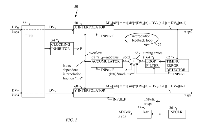
second stage modulus (modulus2) and a second stage seed (seed2) to generate
second
stage index-dependent interpolation frequency mu's (mu2's) and generate the
overflow2's when the modulus2 is exceeded by the accumulation in a similar
manner
to the above described accumulator 68. In some implementations, the seed2 is
the
clock rate fraction tr/2 times the modulus2. The flag F stops the operation of
the FIFO
274, interpolator 258 and accumulator 278 when the FIFO 52 is invalid.
[0081] The interpolation synchronizer 250 with the two stage interpolation
has the benefit of enabling the timing error detector 62 to operate with
clocking at 2
sps while the data estimator 34 operates with a possibly different clocking
rate of tr
sps. This also enables the ADC's 30 to operate at a free running rate that is
independent of the incoming symbol rate and independent of the selected tr
rate so
that the optical receiver 10 can be used in optical systems with different
symbol rates.
The TED interpolator 258 interpolates between the moving interpolations MIx
synchronized to tr sps (in the data domain) to provide to the moving
interpolations
MIXZ synchronized to 2 sps (in the data domain).
[0082] FIGS. 9A and 9B are block diagrams showing an example of the
operation of the FIFO 52 for the interpolation synchronizer circuits 50 and
250. The
X part of the FIFO 52 is referred to as FIFO 52x. The X FIFO 52x is 21K in
length.
The digital values DVx are written into the X FIFO 52x at addresses provided
by a
write counter 288 with an address word (WrAddr) length of K bits. The digital
values
DVx are read by the X interpolator 58 at overflows of the accumulator 68 at
read
address words (RdAddr) provided by a read counter 289 or as a part of an
overflow
word from the accumulator 68. The interpolation fraction mu generated by the
accumulator 68 has length of N bits. Where the read counter 289 is used to
generate
23
WO 2011/059741 PCT/US2010/054485
the read address the accumulator 68 and the seed word have lengths of N bits.
Where
the overflow word is used to generate the read address the accumulator 68 and
the
seed word have N+K bits.
[0083] The reader may refer to the numerical example FIG. 3 and the flow
charts of FIGS. 4-7 and accompanying written descriptions for additional
details for
the block diagrams of the FIGS. 1, 2, 8, and 9A-B; and conversely refer to the
block
diagrams of the FIGS. 1, 2, 8 and 9A-B, and numerical example FIG. 3 and
accompanying written descriptions for additional details for the flow charts
of FIGS.
4-7.
[0084] While this document contains many specifics, these should not be
construed as limitations on the scope of any invention or of what may be
claimed, but
rather as descriptions of features specific to particular embodiments. Certain
features
that are described in this document in the context of separate embodiments can
also be
implemented in combination in a single embodiment. Conversely, various
features
that are described in the context of a single embodiment can also be
implemented in
multiple embodiments separately or in any suitable subcombination. Moreover,
although features may be described above as acting in certain combinations and
even
initially claimed as such, one or more features from a claimed combination can
in
some cases be excised from the combination, and the claimed combination may be
directed to a subcombination or variation of a subcombination. Similarly,
while
operations are depicted in the drawings in a particular order, this should not
be
understood as requiring that such operations be performed in the particular
order
shown or in sequential order, or that all illustrated operations be performed,
to achieve
desirable results.
[0085] Only a few examples and implementations are disclosed. Variations,
modifications and enhancements to the described examples and implementations
and
other implementations may be made based on what is disclosed and illustrated
in this
document.
24