Note: Descriptions are shown in the official language in which they were submitted.
CA 02779468 2012-06-08
FRAME FOR A DEVICE MOUNTED ABOVE A PRINTED CIRCUIT BOARD IN
AN ELECTRONIC DEVICE
FIELD OF DISCLOSURE
[0001] The disclosure relates to a frame for a device (such as a display) for
an electronic device
(such as a portable communication device), in particular, the disclosure
relates to a display
frame mountable on a printed circuit board (PCB) of a communication device,
which provides
electrical shielding to components located underneath the frame.
BACKGROUND OF DISCLOSURE
[0002] In an electronic device, such as a portable phone, a display is
invariably part of the
device. Software operating on the device controls the display to selectively
show information to
the user, such as the current time, caller ID, pictures and battery level.
Typically, a large display
is installed in order to provide larger and clearer pictures, text and
indicators to the user. It is
common for a display to be directly mounted to a top housing portion of the
device leaving the
bottom surface of the display suspended above a printed circuit board located
inside the
housing of the device. However, devices such as portable phones continue to
decrease in size,
the overall size of the housing is shrinking and the distance between the
bottom of the display
and the top of the PCB decreases. This smaller space impinges on the ability
to place
components on the area of the PCB directly underneath the display.
[0003] There is a need to have a system for mounting a component of an
electronic device
(such as a display for a portable phone), which addresses deficiencies in the
prior art.
SUMMARY OF DISCLOSURE
[0004] In a first aspect, a frame for mounting a device above a printed
circuit board (PCB) in
within a housing of an electronic device is provided. The frame comprises a
frame section and
a cover. The frame section is formed to be located on the PCB surrounding a
surface device on
a surface of the PCB is securable to the PCB. The cover is for placement on
top of the frame
section and for providing a support substrate for the device. The cover has a
raised region to
allow a part of the surface device to jut above the frame section; and is
locatable on the frame
section with the device mounted to the cover.
CA 02779468 2012-06-08
- 2 -
[0005] The cover may further have a depressed region to receive a feature on
the bottom of the
device to allow the feature to extend into an interior cavity bounded by the
frame section.
[0006] The feature extending from the bottom of the device may not be located
above the
surface device.
[0007] Each of the cover and the frame section may be comprised of an
electrically conductive
material such that the cover and the frame may provide an electrical contact
for the device to a
ground plane on the PCB providing an electric shield to the surface device.
[0008] The device may be a display device; and the cover may have at least one
electrically
conductive flange extending upward to contact a bottom of the device.
[0009] The frame may have a first post which interacts with the PCB to secure
the frame to the
PCB.
[0010] The cover may have a second post which interacts with the first post to
secure the cover
to the frame.
[0011] The frame section may comprise at least one oblong section shaped to
rest on the PCB.
[0012] The frame section may not define a closed perimeter around the surface
device.
[0013] The frame section may comprise a plurality of bars. The plurality of
bars may be
connected to define an oblong cavity surrounding the surface device.
[0014] The plurality of bars may not define a closed perimeter around the
surface device.
[0015] The frame and cover may combine to provide radio frequency (RF)
shielding for the
surface device.
[0016] In a second aspect, an electronic device is provided, comprising a
housing, a PCB
having a surface device mounted on a surface of the PCB, a frame section and a
cover both for
installation within the housing. The frame section is formed to be located on
the PCB
surrounding the surface device and is securable to the PCB. The cover is for
placement on top
of the frame section and for providing a support substrate for a second
device. The cover has a
raised region to allow a part of the surface device to jut above the frame
section; and is
locatable on the frame section with the second device mounted to the cover
with the surface
device located at least partially underneath the cover.
[0017] The cover may further have a depressed region to receive a feature on
the bottom of the
second device to allow the feature to extend into an interior cavity bounded
by the frame
CA 02779468 2012-06-08
- 3
section. The feature extending from the bottom of the second device may not be
located above
the surface device.
[0018] Each of the cover and the frame section may be comprised of an
electrically conductive
material such that the cover and the frame provide an electrical contact for
the second device to
a ground plane on the PCB providing an electric shield to the surface device.
[0019] The second device may be a display device; and the cover may have at
least one
electrically conductive flange extending upward to contact the bottom of the
second device.
[0020] The frame may have a first post which interacts with the PCB to secure
the frame to the
PCB.
[0021] The cover may have a second post which interacts with the first post to
secure the cover
to the frame.
[0022] The frame section may comprise at least one oblong section shaped to
rest on the PCB.
[0023] The frame section may comprise a plurality of bars. The plurality of
bars may be
connected to define an oblong cavity surrounding the surface device.
[0024] The frame section may define a closed perimeter around the surface
device.
[0025] The plurality of bars may not define a closed perimeter around the
surface device.
[0026] The frame and cover may combine to provide RF shielding for the surface
device.
[0027] In another aspect, a frame for mounting a device above a PCB in an
electronic device is
provided. The frame comprises: a frame section formed to be located on the PCB
about a
surface device on a section of the PCB; and a cover for placement on top of
the frame section
and for providing a support substrate for the device. In the frame, the frame
section is securable
to the PCB above at least a part of the surface device; the cover is locatable
on the frame
section with the device mounted to the cover; and the cover is shaped to allow
a feature on the
bottom of the device to extend downward towards an interior cavity of the
frame.
[0028] In the frame, the cover and the frame section may be comprised of an
electrically
conductive material such that the cover and the frame provide an electrical
contact for the
device to a ground plane on the PCB and provide an electric shield to the
surface device.
[0029] In the frame, the device may be a display device; and the cover may
have an electrically
conductive flange extending upward to contact a bottom of the device.
CA 02779468 2012-06-08
- 4
[0030] In the frame, the frame device may have a first post which interacts
with the PCB to
secure the frame to the PCB; and the cover may have a second post which
interacts with the
first post to secure the cover to the frame.
[0031] In the frame, the feature extending from the bottom of the device maybe
placed in a location which is not above the surface device.
[0032] In yet another aspect, a PCB assembly for an electronic device is
provided. The
assembly comprises: a PCB having a surface device mounted on a section of the
PCB; a frame
section formed to be located on the PCB above the surface device; a cover for
placement on
top of the frame section; and a device mounted on the cover. In the assembly,
when the frame
section is secured to the PCB about the surface device and the cover is
located on the frame
section and the device is mounted to the cover, the surface device is located
at least partially
underneath the cover.
[0033] In the assembly, both the cover and the frame section may be comprised
of an
electrically conductive material such that the cover and the frame provide an
electrical contact
for the device to a ground plane on the PCB.
[0034] In the assembly, the device is may be display device; and the cover may
have
at least one electrically conductive flange extending upward to contact a
bottom of the device.
[0035] In the assembly, the frame may have a first post which interacts with
the PCB to secure
the frame to the PCB, and the cover may have a second post which interacts
with the first post
to secure the cover to the frame.
[0036] In the assembly, the cover may be shaped to allow a feature on the
bottom of the device
to extend downward towards an interior cavity of the frame.
[0037] In the assembly, the feature extending from the bottom of the device
may be placed in a
location which is not above the surface device.
[0038] In other aspects various combinations of sets and subsets of the above
aspects are
provided.
BRIEF DESCRIPTION OF DRAWINGS
[0039] The foregoing and other aspects of the disclosure will become more
apparent from the
following description of specific embodiments thereof and the accompanying
drawings which
illustrate, by way of example only, the principles of the disclosure. In the
drawings, where like
CA 02779468 2012-06-08
- 5 -
elements feature like reference numerals (and wherein individual elements bear
unique
alphabetical suffixes):
[0040] Fig. 1 is a front view of a communication device having a display
internally
mounted to a display frame relating to an embodiment;
[0041] Fig. 2 is a block diagram of internal elements of the device of Fig.
1;
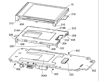
[0042] Fig. 3 is a top perspective view of a portion of an assembled and
populated PCB,
a display and the display frame of the device of Fig. 1;
[0043] Fig. 4 is a top exploded perspective view of the PCB, the display
and the display
frame of Fig. 3;
[0044] Fig. 5A is a bottom perspective view of a central portion of the
display frame of Fig.
3;
[0045] Figs. 5B-5E are bottom perspective views of portions of the display
frame of Fig. 3;
[0046] Fig. 6 is a bottom exploded perspective view of the display and the
display frame
of Fig. 3; and
[0047] Fig. 7 is a top exploded perspective view of the display frame of
Fig. 1 and
aspects of its construction.
DETAILED DESCRIPTION
[0048] The description that follows, and the embodiments described therein,
are provided by
way of illustration of an example, or examples, of particular embodiments of
the principles of the
present disclosure. These examples are provided for the purposes of
explanation, and not
limitation, of those principles and of the disclosure. In the description,
which follows, like parts
are marked throughout the specification and the drawings with the same
respective reference
numerals.
[0049] Fig. 1 schematically illustrates a handheld mobile communication device
10 and its
components, including a housing 12, an input device (e.g. keyboard 14) and an
output device (a
display 16), which is preferably a graphic Liquid Crystal Display (LCD),
although other types of
output devices may alternatively be utilized. Components include electrical
and electronic
devices. Typically, housing 12 is a molded polycarbonate structure and may be
formed via
known plastic injection moulding techniques. To assist in assembly of device
10, housing 12
typically comprises two or more pieces which fit together in a fitted
arrangement to enclose the
CA 02779468 2012-06-08
- 6 -
internal devices and form an exterior casing for device 10. For example,
housing 12 may
comprise an upper housing and a lower housing. Physically for device 10,
housing 12 may be
elongated vertically, or may take on other sizes and shapes (including
clamshell housing
structures).
[0050] Referring to Fig. 2, a processing device (a microprocessor 18) is shown
schematically as
coupled between keyboard 14, display 16 and a series of other internal devices
to device 10.
The microprocessor 18 controls the operation of the display 16, as well as the
overall operation
of the device 10, in response to actuation of keys on the keyboard 14 or
thumbwheel 14B by a
user. Exemplary microprocessors for microprocessor 18 include Data 950 (trade-
mark) series
microprocessors and the 6200 series microprocessor, both available from Intel
Corporation.
[0051] In addition to the microprocessor 18, other internal devices of the
device 10 are shown
schematically in Fig. 2. These devices include: a communication subsystem 100,
a short-range
communication subsystem 102, a set of auxiliary I/0 devices 106, a serial port
108, a speaker
110 and a microphone 112. Memory for device 10 is provided in flash memory 116
and
Random Access Memory (RAM) 118. Internal devices are enclosed within housing
12 and
typically are either mounted onto a printed circuit board (PCB), affixed to an
interior part of the
housing or suspended by some means within housing 12.
[0052] The device 10 is preferably a two-way radio frequency (RF)
communication device
having voice and data communication capabilities. In addition, device 10
preferably has the
capability to communicate with other computer systems via the Internet.
[0053] Operating system software executed by the microprocessor 18 is
preferably stored in a
computer readable medium, such as flash memory 116, but may be stored in other
types of
memory devices, such as read only memory (ROM) or similar storage element. In
addition,
system software, specific device applications, or parts thereof, may be
temporarily loaded into a
volatile store, such as RAM 118. Communication signals received by the mobile
device may
also be stored to RAM 118.
[0054] Microprocessor 18, in addition to its operating system functions,
enables execution of
software applications on device 10. A set of software applications that
control basic device
operations, such as a voice communication module 130A and a data communication
module
130B, may be installed on the device 10 during manufacture or downloaded
thereafter. Cell
mapping module 130C may also be installed on device 10 during manufacture. As
well,
additional software modules, illustrated as an other software module 130N,
which may be, for
CA 02779468 2012-06-08
- 7 -
instance, a personal information manager (PIM) application, may be installed
during
manufacture or downloaded thereafter into device 10. PIM application is
preferably capable of
organizing and managing data items, such as e-mail messages, calendar events,
voice mail
messages, appointments, and task items. PIM application is also preferably
capable of sending
and receiving data items via a wireless network 140.
[0055] Communication functions, including data and voice communications, are
performed
through the communication subsystem 100, and possibly through the short-range
communication subsystem 102. Communication subsystem 100 includes receiver
150,
transmitter 152 and one or more antennae, illustrated as receive antenna 154
and transmit
antenna 156. In addition, communication subsystem 100 also includes processing
module, such
as digital signal processor (DSP) 158 and local oscillators (L0s) 160. The
specific design and
implementation of communication subsystem 100 is dependent upon the
communication
network in which device 10 is intended to operate. For example, communication
subsystem 100
of the device 10 may be designed to operate with the Mobitex (trade-mark),
DataTAC (trade-
mark) or General Packet Radio Service (GPRS) mobile data communication
networks and also
designed to operate with any of a variety of voice communication networks,
such as Advanced
Mobile Phone Service (AMPS), Time Division Multiple Access (TDMA), Code
Division Multiple
Access CDMA, Personal Communication Service (PCS), Global System for Mobile
Communication (GSM), etc. Other types of data and voice networks, both
separate and
integrated, may also be utilized with device 10. It will be appreciated that
some signals received
and transmitted through the subsystem 100 may provide interfering signals with
other
components in device 10, such as microphone 112.
[0056] Network access requirements vary depending upon the type of
communication system
which can communicate with device 10. For example, in the Mobitex (trade-mark)
and DataTAC
(trade-mark) networks, mobile devices are registered on the network using a
unique Personal
Identification Number (PIN) associated with each device. In GPRS networks,
however, network
access is associated with a subscriber or user of a device. A GPRS device
therefore requires a
subscriber identity module, commonly referred to as a Subscriber Identity
Module (SIM) card, in
order to operate on a GPRS network.
[0057] When required network registration or activation procedures have been
completed,
device 10 may send and receive communication signals over communication
network 140.
Signals received from communication network 140 by the receive antenna 154 are
routed to
receiver 150, which provides for signal amplification, frequency down
conversion, filtering,
CA 02779468 2012-06-08
- 8 -
channel selection, etc., and may also provide analog to digital conversion.
Analog-to-digital
conversion of received signals allows the DSP 158 to perform more complex
communication
functions, such as signal demodulation and decoding. In a similar manner,
signals to be
transmitted to network 140 are processed (e.g., modulated and encoded) by DSP
158 and are
then provided to transmitter 152 for digital to analog conversion, frequency
up conversion,
filtering, amplification and transmission to communication network 140 (or
networks) via the
transmit antenna 156.
[0058] In addition to processing communication signals, DSP 158 provides for
control of
receiver 150 and transmitter 152. For example, gains applied to communication
signals in
receiver 150 and transmitter 152 may be adaptively controlled through
automatic gain control
algorithms implemented in DSP 158.
[0059] In a data communication mode, a received signal, such as a text message
or web page
download, is processed by the communication subsystem 100 and is input to
microprocessor
18. The received signal is then further processed by microprocessor 18 for an
output to the
display 16, or alternatively to some other auxiliary I/0 devices 106. A device
user may also
compose data items, such as e-mail messages, using keyboard (keypad) 14,
and/or some other
auxiliary I/0 device 106, such as a touchpad, a thumb-wheel, a rocker switch
or some other
type of input device. The composed data items may then be transmitted over
communication
network 140 via communication subsystem 100.
[0060] In a voice communication mode, overall operation of device 10 is
substantially similar to
the data communication mode, except that received signals are output to
speaker 110, and
received audio signals are provided to microphone 112 for further conversion
into an electrical
signal and further processing by device 10. Microphone 112 is preferably a
silicon-based
transducer which can be mounted to PCB 302 (shown in Fig. 3).
[0061] Short-range communication subsystem 102 enables communication between
device 10
and other proximate systems or devices, which need not necessarily be similar
devices. For
example, the short-range communication subsystem may include an infrared
device and
associated circuits and components, or a Bluetooth (trade-mark) communication
module to
provide for communication with similarly-enabled systems and devices.
[0062] Powering the entire electronics of the mobile handheld communication
device is power
source 170. Preferably, the power source 170 includes one or more batteries.
More preferably,
CA 02779468 2012-06-08
- 9 -
the power source 170 is a single battery pack, especially a rechargeable
battery pack. Power
switch 172 provides a separate on/off switch for device 10.
[0063] Referring to Figs. 1 and 3, further detail on aspects of housing 12 and
internal devices of
device 10 are shown. First, PCB 302 provides a substrate for mounting and
supporting the
internal surface devices on both of its upper and bottom sides and provides
some electrical
circuitry for the devices, as defined by etchings within the layers of plastic
and copper. As such,
devices can be more densely packed thereon, thereby reducing the size of PCB
302. PCB 302
is securely mountable within housing 12, typically via screws which are
threaded through
mounting holes in PCB 302 into receiving threaded ports in the interior of
housing 12.
Alternatively, it may be snap fit to housing 12 with appropriate snap-fit
tangs extending from
PCB 302 to corresponding mounting locations in housing 12. PCB 302 is a
generally planar
sandwich of layers of plastic (or FR4) and copper.
[0064] Referring to Fig. 3, further detail is shown on internal elements of
device 10. In
particular, view 300 shows PCB 302 shown in perspective view having components
mounted
thereon collectively indicated as components 304. Such components 304 include
the physical
devices embodying elements of the modules described in Fig. 2. Components 304
are located
on the top side and bottom side of PCB 302. Display 16 is a generally oblong
and relatively thin
vertical height and is fixedly attached to PCB 302 with a spaced relationship
defined between
the upper surface of PCB 302 and the bottom surface of display 16. Display
frame 306 is
mounted between display 16 and PCB 302, providing the spaced relationship to
PCB 302. As
shown, display frame 306 is fixedly mounted to PCB 302 via posts, provided as
snap-hooks
308. Display 16 mounts on top of display frame 306 and also snap fits to PCB
302 via another
set of posts, provided as snap-hooks 310.
[0065] Referring to Fig. 4, further detail on the space relationship amongst
display 16, frame
306 and PCB 302 is provided. As is shown, on PCB 302, components 304A are
directly
underneath frame 306. Frame 306 is shaped to allow components 304A to be
located on PCB
302 within a region underneath frame 306 and allows display 16 to be mounted
above
component 304A. The major components of frame 306 are a set of four generally
oblong bars
400 arranged to define a flat, generally oblong frame. As such, frame 306
defines an internal
cavity (not shown) whose exterior boundaries are generally defined by bars
400. Frame 306
also has cover 312 attached to the top surface of frame 306. In the
embodiment, cover 312 is
made of a heat and electrically conductive material, such as metal. While
cover 312 is generally
flat, it has surface features including depressed region 314A and raised
region 314B. Regions
CA 02779468 2014-12-23
- 10 -
314A and 314B are shaped and contoured to complement shapes and contours of
features
(such as components 16B, Fig. 6) present on the bottom side of display 16 and
shapes and
contours formed by components 304A. As such, components 16B (Fig. 6) in the
bottom side of
display 16 jut into depressed region 314A and components 304A jut into raised
region 314B. As
such the bottom side of display 16 sits generally flush against cover 312,
while providing
sufficient minimal clearance between the bottom of display 16 and the top of
components 304A.
When display 16 is mounted to frame 306 and both frame 306 and display 16 are
mounted to
PCB 302, frame 306 lies flat against PCB 302 and display 16 lies flat against
frame 306.
[0066] It is notable that frame 306 is shaped and positioned such that within
its
interior space, components 304A take up a portion of the space and depressed
region 314A is
shaped descend from a top surface of frame 306 and is shaped to fit in a
region which does not
overlap with components 304A. As such, display 16 can be placed closer to PCB
302, with the
height of frame 306 selected accordingly, in contrast to a situation where
depressed region
314A is located above components 304A.
[0067] It will be appreciated that frame 306 when mounted to PCB 302 provides
structural
rigidity to PCB 302.
[0068] Referring to Fig. 4, Figs. 5A-E, Fig. 6 and Fig. 7, in the embodiment,
frame 306 is
mounted to PCB 302 via a friction fit arrangement. In particular, snap hooks
308 are located in
each corner of frame 306 and extend vertically downward from its corner. Each
snap hook 308
has a horizontally extending hook 408 at its bottom. In PCB 302, for each snap
hook 308, there
is a corresponding notch 402 in PCB 302 allowing at least a portion of the
corresponding snap
hook 308 to engage a side and bottom of PCB 302. It will be appreciated that
in other
embodiments, the location and number of snap hooks 308 and notches 402 can be
modified to
suit dimensions of the environment.
[0069] In the embodiment, display 16 is mounted about frame 306 to PCB 302 via
a friction fit
arrangement. In particular, snap hooks 310 are located about each corner of
display 16 at a
location which allows it to engage a part of snap hook 308 on frame 306. Each
snap hook 310
extends vertically downward from its corner and has an inward horizontally
extending hook 404
at its bottom. For each snap hook 310, there is a corresponding notch 406 in
snap hook 308
allowing a portion of snap hook 310 to mate against a side of the
corresponding snap hook 308.
Further the snap hook 310 is sized to extend downward below frame 306 such
that its hook 404
can either a notch in snap hook 308, a side and bottom of PCB 302 or both snap
hook 308 and
PCB 302. It will be appreciated that in other embodiments, the location, shape
and number of
1 84607/44461 4
MT DOCS 11528661v3
CA 02779468 2014-12-23
- 11 -
snap hooks 310 and notches 406 can be modified as required using techniques
known in the
art. Posts 322 in frame 306 are located at spaced positions on the bottom of
frame 306 and
extend downward. For each post 322, there is a mating opening in PCB 302,
thereby providing
an alignment mechanism for mating frame 306 to PCB 302. In another embodiment,
a post 322
makes an electrical connection with an internal copper layer in PCB 302. In
other
embodiments, other fastening mechanisms may be used to secure frame 306 to PCB
302,
including screws and binding posts, glue or other techniques known in the art.
[0070] Turning back to display 16, its electrical connector 318 is shown
extending from a
bottom side of an end of display 16. In use, connector 318 mates with
connector 320 on PCB
302. Connector 320 has internal wires connected to copper traces on PCB 302,
thereby
providing electrical contact for control of display 16. As frame 306 is shaped
to have
approximately the same footprint of display 16 and as connector 318 extends
from the bottom of
display 16, notch 410 (Fig. 7) is provided in frame 306 at a region where
connector 318 would
extend downward from display 16, when display 16 is mounted to frame 306.
Notch 410 is
shaped to allow connector 318 access to connector 320 and allow display 16 to
be mounted flat
against frame 306.
[0071] Referring to Figs. 6 and 7, further detail is provided on aspects of
frame 306 and display
16. Frame 306 has four bars 400 to define the exterior perimeter and interior
cavity 500
associated with frame 306. Cover 312 is shaped to fit flush with the exterior
dimensions of
frame 306. Cover 312 is securely attached to frame 306. In the embodiment,
adhesive strip
502 is a shaped doubled sided adhesive tap shaped to fit on the top surface of
bars 400. As
such, when cover 312 is placed on top of frame 306, adhesive strip 502 binds
to both frame 306
and cover 312. Also, cover 312 has snap-fit tabs 504 which provide a friction
fit mating
arrangement with corresponding snap-regions 506 on frame 306. Each snap-region
506 is
shaped to receive at least a portion of a side of its corresponding snap-fit
tab 504. Further, rails
508 on bars 400 extend upwardly from the exterior sides of bars 400 and
provide a set of
alignment rails to assist in guiding the positioning of cover 312 as it is
being place on frame 306.
[0072] Also, adhesive strip 510 is a shaped doubled sided adhesive tape shaped
to fit on the
bottom surface of bars 400. As such, when frame 306 is mounted to PCB 302, in
addition to the
snap-fit provided by snap hooks 308 gripping portions of PCB 302, strip 510
provides a further
securement mechanism to fix frame 306 to PCB 302.
184607/444614
MT DOCS 11528661v3
CA 02779468 2012-06-08
- 12
[0073] As noted, display 16 has connector 318 located on the bottom surface
about one end
thereof As such, bar 400A has depression 316 formed therein to allow connector
318 to fit
against frame 306.
[0074] The embodiment also provides enhanced electrical grounding for display
16. In
particular, on cover 312, around either side of the corresponding opening
around depression
316, flanges 512 extend vertically upward. Flanges 512 make friction contact
with the bottom of
display 16 when display 16 is mounted on cover 312 and are shaped and located
on cover 312
such that the extended end of flanges 510 contact a grounded metal section on
the bottom of
display 16, thereby making an electrical connection between cover 312 and the
bottom of
display 16. In the embodiment, frame 306 is composed of a plastic material
such as PVC or
any suitable plastic material. In addition, frame 306 may have a metal plating
which is in
contact with cover 312. Also, frame 306 may contain metallic particles therein
or may have
metallic shunts or connections therein which contact cover 312. On the surface
layer of PCB
302, electrical contact points may be provided which connect a ground plane in
PCB 302 to any
such shunts or connections or frame 306 itself. In the embodiment, adhesive
strips 502 and
510 are conductive, thereby enhancing electrical contacts between frame 306
and PCB 302. As
such, a direct electrical connection is provided from the bottom of display 16
to the ground plane
of PCB 302.
[0075] Further still, the embodiment also provides electrical shielding from
external RF signals
for components located under frame 306, such as components 304A, on PCB 302.
The
electrical shielding is provided from an electrical cage formed from the
electrical portion of the
bottom of display 16 in contact with cover 312 in contact with adhesive strip
502 in contact with
conductive portions of frame 306 in contact with adhesive strip 510 in contact
with selected
ground tracks in PCB 302. To facilitate electrical connections between frame
306 and cover
312, in one embodiment, frame 306 is covered with a metal plate and in another
embodiment, it
is metal plated.
[0076] It will be appreciated that in other embodiments, frame 306 may be
replaced by a frame
and bars having different shapes and sizes. For example, frame 306 and cover
312 may be
formed as a single piece. Also, the other frame may be provided in two or more
pieces. Also,
the other frame may be one piece, which does not define a closed perimeter.
Also, frame 306
may be replaced by a series of posts or similar singular structures.
[0077] It will be appreciated that although the embodiments have been shown
being used with
a communication device, such as a portable phone, it is possible to use any
embodiment in any
CA 02779468 2012-06-08
- 13 -
device having electrical components. Further, any embodiment may be used to
provide a
spaced relationship for any component to PCB, not necessarily just a display.
It will be
appreciated that the term frame may be used generically to describe a system
comprising a
frame (such as frame 306) with a cover (such as cover 312). In such use, the
frame portion
may be identified as a frame section of the frame.
[0078] Although the disclosure has been described with reference to certain
specific
embodiments, various modifications thereof will be apparent to those skilled
in the art without
departing from the scope of the disclosure as outlined in the claims appended
hereto.