Note: Descriptions are shown in the official language in which they were submitted.
CA 02779609 2017-02-17
Extremely Low Resistance Films and
Methods for Modifying or Creating Same
(01)
Field of the Invention
(02) The invention is generally related to films or tapes with extremely low
resistance
("ELR films" or "ELR tapes") at high temperatures, and more particularly to
modifying
existing ELR films and/or creating new ELR films that operate with improved
operating
characteristics.
Background of the Invention
(03) Ongoing research attempts to achieve new materials with improved
operational
characteristics, for example, reduced electrical resistance at higher
temperatures over
existing materials, including superconducting materials. Scientists have
theorized a
possible existence of a "perfect conductor," or a material that operates with
extremely low
resistance, but that may not necessarily demonstrate all the conventionally
accepted
characteristics of a superconducting material.
(04) Notwithstanding their name, conventional high temperature superconducting
("FITS") materials still operate at very low temperatures. In fact, most
commonly used
HTS materials still require use of a cooling system that uses liquids with
very low boiling
points (e.g., liquid nitrogen). Such cooling systems increase implementation
costs and
discourage widespread commercial and consumer use and/or application of such
materials.
- -
CA 02779609 2012-05-01
WO 2011/041764 PCT/US2010/051239
(05) What is needed are ELR films with improved operating characteristics;
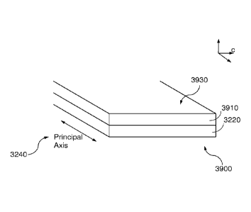
mechanisms for modifying known ELR films so that the modified ELR films
operate with
improved operating characteristics; and/or techniques for designing and
fabricating new
ELR films.
Brief Description of the Drawings
(06) The accompanying drawings, which are included to provide a further
understanding of the invention and are incorporated in and constitute a part
of this
specification, illustrate various exemplary implementations of the invention
and together
with the detailed description serve to explain various principles and/or
aspects of the
invention.
(07) Figure 1 illustrates a crystalline structure of an exemplary ELR material
as viewed
from a first perspective.
(08) Figure 2 illustrates a crystalline structure of an exemplary ELR material
as viewed
from a second perspective.
(09) Figure 3 illustrates a crystalline structure of an exemplary ELR material
as viewed
from a second perspective.
(10) Figure 4 illustrates a conceptual mechanical model of a crystalline
structure of an
ELR material.
(//) Figure 5 illustrates a conceptual mechanical model of an improved
crystalline
structure, according to various implementations of the invention, of an ELR
material.
(12) Figure 6 illustrates a conceptual mechanical model of an improved
crystalline
structure, according to various implementations of the invention, of an ELR
material.
(13) Figure 7 illustrates a conceptual mechanical model of an improved
crystalline
structure, according to various implementations of the invention, of an
exemplary ELR
material.
- 2 -
CA 02779609 2012-05-01
WO 2011/041764 PCT/US2010/051239
(14) Figure 8 illustrates a conceptual mechanical model of an improved
crystalline
structure, according to various implementations of the invention, of an ELR
material.
(15) Figure 9 illustrates a conceptual mechanical model of an improved
crystalline
structure, according to various implementations of the invention, of an ELR
material.
(16) Figure 10 illustrates a modified crystalline structure, according to
various
implementations of the invention, of an ELR material as viewed from a second
perspective.
(17) Figure 11 illustrates a modified crystalline structure, according to
various
implementations of the invention, of an ELR material as viewed from a first
perspective.
(18) Figure 12 is a flowchart for producing a modified material from an ELR
material
according to various implementations of the invention.
(19) Figures 13A-13J illustrate preparing a modified ELR material according to
various
implementations of the invention.
(20) Figure 14 is a flowchart for depositing a modifying material onto an ELR
material
according to various implementations of the invention.
(21) Figure 15 illustrates a test bed useful for determining various
operational
characteristics of a modified ELR material according to various
implementations of the
invention.
(22) Figures 16A-16G illustrate test results demonstrating various operational
characteristics of a modified ELR material.
(23) Figure 17 illustrates a crystalline structure of an exemplary ELR
material as viewed
from a second perspective.
(24) Figure 18 illustrates a crystalline structure of an exemplary ELR
material as viewed
from a second perspective.
- 3 -
CA 02779609 2012-05-01
WO 2011/041764 PCT/US2010/051239
(25) Figure 19 illustrates a crystalline structure of an exemplary ELR
material as viewed
from a second perspective.
(26) Figure 20 illustrates an arrangement of an ELR material and a modifying
material
useful for propagating electrical charge according to various implementations
of the
invention.
(27) Figure 21 illustrates a single unit cell of an exemplary ELR material.
(28) Figure 22 illustrates a crystalline structure of an exemplary ELR
material as viewed
from a second perspective.
(29) Figure 23 illustrates multiple layers of crystalline structures of an
exemplary
surface-modified ELR material according to various implementations of the
invention.
(30) Figure 24 illustrates test results demonstrating various operational
characteristics
of a modified ELR material, namely with chromium as a modifying material and
YBCO as
an ELR material, in accordance with various implementations of the invention.
(31) Figure 25 illustrates test results demonstrating various operational
characteristics
of a modified ELR material, namely with vanadium as a modifying material and
YBCO as
an ELR material, in accordance with various implementations of the invention.
(32) Figure 26 illustrates test results demonstrating various operational
characteristics
of a modified ELR material, namely with bismuth as a modifying material and
YBCO as an
ELR material, in accordance with various implementations of the invention.
(33) Figure 27 illustrates test results demonstrating various operational
characteristics
of a modified ELR material, namely with copper as a modifying material and
YBCO as an
ELR material, in accordance with various implementations of the invention.
(34) Figure 28 illustrates test results demonstrating various operational
characteristics
of a modified ELR material, namely with cobalt as a modifying material and
YBCO as an
ELR material, in accordance with various implementations of the invention.
- 4 -
CA 02779609 2012-05-01
WO 2011/041764 PCT/US2010/051239
(35) Figure 29 illustrates test results demonstrating various operational
characteristics
of a modified ELR material, namely with titanium as a modifying material and
YBCO as an
ELR material, in accordance with various implementations of the invention.
(36) Figure 30 illustrates a crystalline structure of an exemplary ELR
material as viewed
from a third perspective.
(37) Figure 31 illustrates a reference frame useful for describing various
implementations of the invention.
(38) Figure 32 illustrates a c-film of ELR material according to various
implementations
of the invention.
(39) Figure 33 illustrates a c-film with appropriate surfaces of ELR material
according to
various implementations of the invention.
(40) Figure 34 illustrates a c-film with appropriate surfaces of ELR material
according to
various implementations of the invention.
(41) Figure 35 illustrates a modifying material layered onto appropriate
surfaces of ELR
material according to various implementations of the invention.
(42) Figure 36 illustrates a modifying material layered onto appropriate
surfaces of ELR
material according to various implementations of the invention.
(43) Figure 37 illustrates a c-film with an etched surface including
appropriate surfaces
of ELR material according to various implementations of the invention.
(44) Figure 38 illustrates a modifying material layered onto an etched surface
of a c-film
with appropriate surfaces of ELR material according to various implementations
of the
invention.
(45) Figure 39 illustrates an a-b film, including an optional substrate, with
appropriate
surfaces of ELR material according to various implementations of the
invention.
- 5 -
CA 02779609 2012-05-01
WO 2011/041764 PCT/US2010/051239
(46) Figure 40 illustrates a modifying material layered onto appropriate
surfaces of ELR
material of an a-b film according to various implementations of the invention.
(47) Figure 41 illustrates various exemplary arrangements of layers of ELR
material,
modifying material, buffer or insulating layers, and/or substrates in
accordance with
various implementations of the invention.
(48) Figure 42 illustrates a process for forming a modified ELR material
according to
various implementations of the invention.
(49) Figure 43 illustrates an example of additional processing that may be
performed
according to various implementations of the invention.
(50) Figure 44 illustrates a process for forming a modified ELR material
according to
various implementations of the invention.
(51) Figure 45 illustrates a crystalline structure of an exemplary ELR
material as viewed
from a second perspective.
(52) Figure 46 illustrates a crystalline structure of an exemplary ELR
material as viewed
from a second perspective.
Summary of the Invention
(53) Generally speaking, various implementations of the invention relate to
modifying
existing ELR materials and/or processes for creating new ELR materials. In
some
implementations of the invention, existing ELR materials are modified to
create modified
ELR materials with improved operating characteristics. These operating
characteristics
may include, but are not limited to, operating in an ELR state (including, for
example, a
superconducting state) at higher temperatures, operating with increased charge
carrying
capacity at the same (or higher) temperatures, operating with improved
magnetic
properties, operating with improved mechanical properties, and/or other
improved
operating characteristics. As will be described in further detail below, for
purposes of this
description, ELR materials comprise: superconducting materials, including HTS
- 6 -
CA 02779609 2012-05-01
WO 2011/041764 PCT/US2010/051239
materials; perfectly conducting materials (e.g., perfect conductors); and
other conductive
materials with extremely low resistance.
(54) In some implementations of the invention, a method comprises layering a
modifying material onto an appropriate surface of an ELR film to create a
modified ELR
film, where the modified ELR film has improved operational characteristics
over those of
the ELR film without the modifying material.
(55) In some implementations of the invention, a method comprises forming an
appropriate surface on or within an ELR film and layering a modifying material
onto the
appropriate surface of the ELR film to create a modified ELR film, where the
modified ELR
film has improved operational characteristics over those of the ELR film alone
or without
the modifying material. In further implementations of in the invention, the
appropriate
surface is not substantially parallel to a c-plane of the ELR film.
(56) In various implementations of the invention, the improved operational
characteristics include operating in an ELR state at higher temperatures,
operating with
increased charge carrying capacity at the same or higher temperatures,
operating with
improved magnetic properties, or operating with improved mechanical
properties.
(57) In some implementations of the invention, layering a modifying material
onto an
appropriate surface of the ELR film comprises depositing the modifying
material onto the
appropriate surface of the ELR film. In further implementations of the
invention,
depositing the modifying material onto the appropriate surface of the ELR film
comprises
using MBE, PLD, or CVD.
(58) In some implementations of the invention, layering a modifying material
onto an
appropriate surface of the ELR film comprises layering the modifying material
onto a face
of the ELR film that is not substantially parallel to a c-plane of a
crystalline structure of an
ELR material in the ELR film. In some implementations of the invention,
layering a
modifying material onto an appropriate surface of the ELR film comprises
layering the
modifying material onto a face of the ELR material that is parallel to an ab-
plane of a
crystalline structure of the ELR material. In some implementations of the
invention,
- 7 -
CA 02779609 2012-05-01
WO 2011/041764 PCT/US2010/051239
layering a modifying material onto appropriate surface of the ELR film
comprises layering
the modifying material onto a face of the ELR material that is parallel to an
a-plane or a
b-plane of a crystalline structure of the ELR material.
(59) In some implementations of the invention, layering a modifying material
onto an
appropriate surface of the ELR film comprises layering chromium, copper,
bismuth, cobalt,
vanadium, titanium, rhodium, beryllium, gallium, or selenium onto the
appropriate surface
of the ELR film.
(60) In some implementations of the invention, forming the appropriate surface
on or
within the ELR film comprises exposing the appropriate surface on or within
the ELR film.
(61) In some implementations of the invention, forming the appropriate surface
on or
within the ELR film comprises layering an ELR material onto a substrate in a
manner that
orients a particular axis of the crystalline structure of the ELR material
along a principal
axis of the substrate, wherein the particular axis is a line within the c-
plane of the
crystalline structure of the ELR material. In further implementations of the
invention, the
particular axis is the a-axis or the b-axis.
(62) In some implementations of the invention, exposing the appropriate
surface of the
ELR film comprises etching a primary surface of the ELR film to increase a
surface area of
the primary surface.
(63) In some implementations of the invention, exposing the appropriate
surface of the
ELR film comprises creating a pattern in a primary surface of the ELR film
thereby
exposing one or more appropriate surfaces of the ELR film.
(64) In some implementations of the invention, creating a pattern in a primary
surface of
the ELR film comprises inscribing a groove in the ELR material of the ELR
film. In some
implementations of the invention, the groove is substantially in the direction
of the
principal axis of the ELR film. In some implementations of the invention, the
groove has a
depth substantially equal to a thickness of the ELR material. In some
implementations of
the invention, the groove has a depth less than a thickness of the ELR
material. In some
implementations of the invention, the width of the at least one groove is
greater than
- 8 -
CA 02779609 2012-05-01
WO 2011/041764 PCT/US2010/051239
1 Onm. In some implementations of the invention, a modifying material is
deposited into
the groove.
(65) In some implementations of the invention, a method comprises creating at
least
one groove in the primary surface of an ELR film, thereby exposing a face of
the ELR film,
the exposed face being a face parallel to an ab-plane of the crystalline
structure of an ELR
material in the ELR film and depositing a modifying material onto the exposed
face.
(66) In some implementations of the invention, depositing a modifying material
onto the
exposed face comprises depositing a single unit layer of the modifying
material onto the
exposed face. In some implementations of the invention, depositing a modifying
material
onto the exposed face comprises depositing two or more unit layers of the
modifying
material onto the exposed face.
(67) In some implementations of the invention, layering a modifying material
onto an
appropriate surface of the ELR film comprises layering the modifying material
onto a face
of the ELR film that is not substantially parallel to a c-plane of the ELR
film.
(68) In some implementations of the invention, a method comprises bonding a
modifying material to an ELR material to form a modified ELR material, where
the
modified ELR material operates at a temperature greater than that of the ELR
material
alone or without the modifying material. In some implementations of the
invention, the
ELR material is a superconducting material.
(69) In some implementations, a modifying material is layered onto an ELR
material to
form a modified ELR material that operates with an improved operating
characteristic
over that of the ELR material alone or without a modifying material. ELR
materials may
be selected from a family of ELR materials referred to as mixed-valence copper-
oxide
perovskites. In some implementations, modifying materials may be selected from
any
one or combination of the following: chromium (Cr), copper (Cu), bismuth (Bi),
cobalt
(Co), vanadium (V), titanium (Ti), rhodium (Rh), beryllium (Be), gallium (Ga),
and/or
selenium (Se).
- 9 -
CA 02779609 2012-05-01
WO 2011/041764 PCT/US2010/051239
(70) In some implementations of the invention, a composite comprises an ELR
material,
and a modifying material bonded to the ELR material such that the composite
operates in
an ELR state at a temperature greater than that of the ELR material alone or
without the
modifying material.
(71) In some implementations of the invention, a composite comprises a first
layer
comprising an ELR material, and a second layer comprising a modifying
material, where
the second layer is bonded to the first layer. In some implementations of the
invention, a
composite comprises a first layer comprising an ELR material, a second layer
comprising
a modifying material, where the second layer is bonded to the first layer, a
third layer
comprising the ELR material, and a fourth layer of the modifying material,
where the third
layer is bonded to the fourth layer. In some implementations of the invention,
the second
layer is deposited onto the first layer. In some implementations of the
invention, the first
layer is deposited onto the second layer. In some implementations of the
invention, the
ELR material of the first layer is formed on the second layer. In some
implementations of
the invention, the first layer has a thickness of at least a single
crystalline unit cell of the
ELR material. In some implementations of the invention, the first layer has a
thickness of
several crystalline unit cells of the ELR material. In some implementations of
the
invention, the second layer has a thickness of at least a single unit (e.g.,
atom, molecule,
crystal, unit cell, or other unit) of the modifying material. In some
implementations of the
invention, the second layer has a thickness of several units of the modifying
material.
(72) In some implementations of the invention, a composite comprises a first
layer
comprising YBCO, and a second layer comprising a modifying material, wherein
the
modifying material of the second layer is bonded to the YBCO of the first
layer, wherein
the modifying material is an element selected as any one or more of the group
including:
chromium, copper, bismuth, cobalt, vanadium, titanium, rhodium, beryllium,
gallium, or
selenium. In some implementations of the invention, the modifying material of
the second
layer is bonded to a face of the YBCO of the first layer, where the face is
substantially
parallel to a c-axis of the YBCO. In some implementations of the invention,
the modifying
material of the second layer is bonded to a face of the YBCO of the first
layer, where the
face is substantially parallel to an ab-plane of the YBCO. In some
implementations of the
- 1 o -
CA 02779609 2012-05-01
WO 2011/041764 PCT/US2010/051239
invention, the modifying material of the second layer is bonded to a face of
the YBCO of
the first layer, where the face is substantially perpendicular to a b-axis of
the YBCO. In
some implementations of the invention, the modifying material of the second
layer is
bonded to a face of the YBCO of the first layer, where the face is
substantially
perpendicular to an a-axis of the YBCO.
(73) In some implementations of the invention, the ELR material comprises a
superconducting material. In some implementations of the invention, the ELR
material
comprises a mixed-valence copper-oxide perovskite material. In some
implementations
of the invention, the mixed-valence copper-oxide perovskite material may be
selected
from the groups generically referred to as LaBaCuO, LSCO, YBCO, BSCCO, TBCCO,
HgBa2Ca2Cu30x, or other mixed-valence copper-oxide perovskite materials. In
some
implementations of the invention, the ELR material comprises an iron pnictide
material. In
some implementations of the invention, the ELR material comprises magnesium
diboride.
In some implementations of the invention, the modifying material may be a
conductive
material. In some implementations of the invention, the modifying material may
be a
material that bonds easily with oxygen. In some implementations of the
invention, the
modifying material may be a conductive material that bonds easily with oxygen
("oxygen
bonding bonding conductive material"). In some implementations of the
invention, the
modifying material may be any one or combination of chromium, copper, bismuth,
cobalt,
vanadium, titanium, rhodium, beryllium, gallium, and/or selenium. In some
implementations of the invention, various combinations of the ELR materials
and the
modifying materials may be used. In some implementations of the invention, the
ELR
material is YBCO and the modifying material is chromium.
(74) In some implementations of the invention, the composite of the ELR
material with
the modifying material operates at a higher temperature than the ELR material
alone or
without the modifying material. In some implementations of the invention, the
composite
demonstrates ELR at a higher temperature than that of the ELR material alone
or without
the modifying material. In some implementations of the invention, the
composite
transitions from a non-ELR state to an ELR state at a temperature higher than
that of the
ELR material alone or without the modifying material. In some implementations
of the
-11-
CA 02779609 2012-05-01
WO 2011/041764 PCT/US2010/051239
invention, the composite has a transition temperature greater than that of the
ELR
material alone or without the modifying material. In some implementations of
the
invention, the composite carries a greater amount of current in an ELR state
than that
carried by the ELR material alone or without the modifying material.
(75) In some implementations of the invention, the composite operates in an
ELR state
at a higher temperature than the ELR material alone or without the modifying
material. In
some implementations of the invention, the composite operates in an ELR state
at
temperatures greater than any one of the following temperatures: 200K, 210K,
220K,
230K, 240K, 250K, 260K, 270K, 280K, 290K, 300K, or 310K.
(76) In some implementations of the invention where the ELR material is YBCO,
the
composite has improved operating characteristics over those of YBCO alone or
without
the modifying material. In some implementations of the invention where the ELR
material
is YBCO, the composite operates at a higher temperature than that of YBCO
alone or
without the modifying material. In some implementations of the invention where
the ELR
material is YBCO, the composite demonstrates extremely low resistance at a
higher
temperature than that of YBCO alone or without the modifying material. In some
implementations of the invention where the ELR material is YBCO, the composite
transitions from a non-ELR state to an ELR state at a temperature higher than
that of
YBCO alone or without the modifying material. In some implementations of the
invention
where the ELR material is YBCO, the composite has a transition temperature
greater than
that of YBCO alone or without the modifying material. In some implementations
of the
invention where the ELR material is YBCO, the composite carries a greater
amount of
current in an ELR state than that carried by YBCO in its ELR state alone or
without the
modifying material.
(77) In some implementations of the invention, an ELR composite comprises a
first
layer comprised of an ELR material, and a second layer comprised of a
modifying
material bonded to the ELR material of the first layer, where the ELR
composite has an
improved operational characteristic over the operational characteristics of
the ELR
material without the modifying material.
- 12 -
CA 02779609 2012-05-01
WO 2011/041764 PCT/US2010/051239
Detailed Description
(78) Various features, advantages, and implementations of the invention may be
set
forth or be apparent from consideration of the following detailed description,
the drawings,
and the claims. It is to be understood that the detailed description and the
drawings are
exemplary and intended to provide further explanation without limiting the
scope of the
invention except as set forth in the claims.
(79) Various implementations of the invention are related to ELR films (which
include
ELR materials), and more particularly to modifying existing ELR films and/or
creating new
ELR films that operate with improved operating characteristics. The novel ELR
films can
encompass, for example, composites, products, processes of manufacture,
product-by-process, methods of making novel ELR films, for example, to obtain
a new
technical effect.
(80) For purposes of this description, extremely low resistance ("ELR")
materials may
include: superconducting materials, including, but not limited to, HTS
materials; perfectly
conducting materials (e.g., perfect conductors); and other conductive
materials with
extremely low resistance. Further, for purposes of this description, operating
characteristics with regard to ELR materials and/or various implementations of
the
invention may include, but are not limited to, a resistance of the ELR
material in its ELR
state (for example, with regard to superconductors, a superconducting state),
a transition
temperature of the ELR material to its ELR state, a charge propagating
capacity of the
ELR material in its ELR state, one or more magnetic properties of the ELR
material, one
or more mechanical properties of the ELR material, and/or other operating
characteristics
of the ELR material. Further, for purposes of this description, "extremely low
resistance"
is resistance similar in magnitude to the flux flow resistance of Type II
superconducting
materials in their superconducting state, and may generally be expressed in
terms of
resistivity in a range of zero Ohm-cm to one fiftieth (1/50) of the
resistivity of substantially
pure copper at 293K. For example, as used herein, substantially pure copper is
99.999%
copper. In various implementations of the invention, portions of modified
and/or new ELR
materials have a resistivity in a range of zero Ohm-cm to 3.36x10⁻⁸ Ohm-cm.
- 13-
CA 02779609 2012-05-01
WO 2011/041764 PCT/US2010/051239
(81) Incremental improvements in a transition temperature (sometimes also
referred to
as a critical temperature) of ELR materials, and in particular,
superconducting materials,
appear to be based on trial and error rather than an understanding of the
mechanisms by
which ELR materials operate. Without such an understanding, further
improvements to a
transition temperature (or other operating characteristic) of the known ELR
materials (or
classes thereof) as well as design of new ELR materials are limited. As
generally
understood, the transition temperature is a temperature below which the ELR
material
"operates" or exhibits (or begins exhibiting) extremely low resistance, and/or
other
phenomenon associated with ELR materials. When operating with extremely low
resistance, the ELR material is referred to as being in an ELR state. At
temperatures
above the transition temperature, the ELR material ceases to exhibit extremely
low
resistance and the ELR material is referred to as being in its non-ELR state.
In other
words, the transition temperature corresponds to a temperature at which the
ELR
material changes between its non-ELR state and its ELR state. As would be
appreciated,
for some ELR materials, the transition temperature may be a range of
temperatures over
which the ELR material changes between its non-ELR state and its ELR state. As
would
also be appreciated, the ELR material may have hysteresis in its transition
temperature
with one transition temperature as the ELR material warms and another
transition
temperature as the ELR material cools.
(82) Figure 31 illustrates a reference frame 3100 which may be used to
describe
various implementations of the invention. Reference frame 3100 includes a set
of axes
referred to as an a-axis, a b-axis, and a c-axis. For purposes of this
description: reference
to the a-axis includes the a-axis and any other axis parallel thereto;
reference to the b-axis
includes the b-axis and any other axis parallel thereto; and reference to the
c-axis
includes the c-axis and any other axis parallel thereto. Various pairs of the
axes form a
set of planes in reference frame 3100 referred to as an a-plane, a b-plane,
and a c-plane,
where: the a-plane is formed by the b-axis and the c-axis and is perpendicular
to the
a-axis; the b-plane is formed by the a-axis and the c-axis and is
perpendicular to the
b-axis; and the c-plane is formed by the a-axis and the b-axis and is
perpendicular to the
c-axis. For purposes of this description: reference to the a-plane includes
the a-plane
and any plane parallel thereto; reference to the b-plane includes the b-plane
and any
- 14 -
CA 02779609 2012-05-01
WO 2011/041764 PCT/US2010/051239
plane parallel thereto; and reference to the c-plane includes the c-plane and
any plane
parallel thereto. Further, with regard to various "faces" or "surfaces" of the
crystalline
structures described herein, a face parallel to the a-plane may sometimes be
referred to
as a "b-c" face; a face parallel to the b-plane may sometimes be referred to
as an "a-c"
face; and a face parallel to the c-plane may sometimes be referred to as a "a-
b" face.
(83) Figure 1 illustrates a crystalline structure 100 of an exemplary ELR
material as
viewed from a first perspective, namely, a perspective perpendicular to an "a-
b" face of
crystalline structure 100 and parallel to the c-axis thereof. Figure 2
illustrates crystalline
structure 100 as viewed from a second perspective, namely, a perspective
perpendicular
to a "b-c" face of crystalline structure 100 and parallel to the a-axis
thereof. Figure 22
illustrates additional depth (i.e., into the page) for crystalline structure
100 of the
exemplary ELR material. For purposes of this description, the exemplary ELR
material
illustrated in Figure 1, Figure 2 and Figure 22 is generally representative of
various ELR
materials. In some implementations of the invention, the exemplary ELR
material may be
a representative of a family of superconducting materials referred to as mixed-
valence
copper-oxide perovskites. The mixed-valence copper-oxide perovskite materials
include,
but are not limited to, LaBaCu0x, LSCO (e.g., La2_xSrxCu04, etc.), YBCO (e.g.,
YBa2Cu307, etc.), BSCCO (e.g., Bi2Sr2Ca2Cu3010, etc.), TBCCO (e.g.,
TI2Ba2Ca2Cu3010
or TImBa2Can_iCun02n,m+2,6), HgBa2Ca2Cu30x, and other mixed-valence copper-
oxide
perovskite materials. The other mixed-valence copper-oxide perovskite
materials may
include, but are not limited to, various substitutions of the cations as would
be appreciated.
As would also be appreciated, the aforementioned named mixed-valence copper-
oxide
perovskite materials may refer to generic classes of materials in which many
different
formulations exist. In some implementations of the invention, the exemplary
ELR
materials may include an HTS material outside of the family of mixed-valence
copper-oxide perovskite materials ("non-perovskite materials"). Such non-
perovskite
materials may include, but are not limited to, iron pnictides, magnesium
diboride (Mg B2),
and other non-perovskites. In some implementations of the invention, the
exemplary ELR
materials may be other superconducting materials. Other materials having an
aperture
- 15-
CA 02779609 2012-05-01
WO 2011/041764 PCT/US2010/051239
210 may be exploited in accordance with various aspects of the invention as
would be
appreciated.
(84) Many ELR materials have a structure similar to (though not necessarily
identical to)
that of crystalline structure 100 with different atoms, combinations of atoms,
and/or lattice
arrangements as would be appreciated. As illustrated in Figure 2, crystalline
structure
100 is depicted with two complete unit cells of the exemplary ELR material,
with one unit
cell above reference line 110 and one unit cell below reference line 110.
Figure 21
illustrates a single unit cell 2100 of the exemplary ELR material.
(85) Generally speaking and as would be appreciated, a unit cell 2100 of the
exemplary
ELR material includes six "faces": two "a-b" faces that are parallel to the c-
plane; two
"a-c" faces that are parallel to the b-plane; and two "b-c" faces that are
parallel to the
a-plane (see, e.g., Figure 31). As would also be appreciated, a "surface" of
ELR material
in the macro sense may be comprised of multiple unit cells 2100 (e.g.,
hundreds,
thousands or more). Reference in this description to a "surface" or "face" of
the ELR
material being parallel to a particular plane (e.g., the a-plane, the b-plane
or the c-plane)
indicates that the surface is formed predominately (i.e., a vast majority) of
faces of unit
cell 2100 that are substantially parallel to the particular plane.
Furthermore, reference in
this description to a "surface" or "face" of the ELR material being parallel
to planes other
than the a-plane, the b-plane, or the c-plane (e.g., an ab-plane as described
below, etc.)
indicates that the surface is formed from some mixture of faces of unit cell
2100 that, in
the aggregate macro sense, form a surface substantially parallel to such other
planes.
(86) Studies indicate that some ELR materials demonstrate an an isotropic
(i.e.,
directional) dependence of the resistance phenomenon. In other words,
resistance at a
given temperature and current density depends upon a direction in relation to
crystalline
structure 100. For example, in their ELR state, some ELR materials can carry
significantly more current, at zero resistance, in the direction of the a-axis
and/or in the
direction of the b-axis than such materials do in the direction of the c-axis.
As would be
appreciated, various ELR materials exhibit anisotropy in various performance
phenomenon, including the resistance phenomenon, in directions other than, in
addition
- 16-
CA 02779609 2012-05-01
WO 2011/041764 PCT/US2010/051239
to, or as combinations of those described above. For purposes of this
description,
reference to a material that tends to exhibit the resistance phenomenon (and
similar
language) in a first direction indicates that the material supports such
phenomenon in the
first direction; and reference to a material that tends not to exhibit the
resistance
phenomenon (and similar language) in a second direction indicates that the
material does
not support such phenomenon in the second direction or does so in a reduced
manner
from other directions.
(87) Conventional understanding of known ELR materials has thus far failed to
appreciate an aperture 210 formed within crystalline structure 100 by a
plurality of
aperture atoms 250 as being responsible for the resistance phenomenon. (See
e.g.,
Figure 21, where aperture 210 is not readily apparent in a depiction of single
unit cell
2100.) As will be further described below, aperture 210 exists in many known
ELR
materials. In some sense, aperture atoms 250 may be viewed as forming a
discrete
atomic "boundary" or "perimeter" around aperture 210. In some implementations
of the
invention and as illustrated in Figure 2, aperture 210 appears between a first
portion 220
and a second portion 230 of crystalline structure 100 although in some
implementations
of the invention, aperture 210 may appear in other portions of various other
crystalline
structures. While aperture 210, aperture 310, and other apertures are
illustrated in Figure
2, Figure 3, and elsewhere in the drawings based on depictions of atoms as
simple
"spheres," it would be appreciated that such apertures are related to and
shaped by,
among other things, electrons and their associated electron densities (not
otherwise
illustrated) of various atoms in crystalline structure 100, including aperture
atoms 250.
(88) According to various aspects of the invention, aperture 210 facilitates
propagation
of electrical charge through crystalline structure 100 and when aperture 210
facilitates
propagation of electrical charge through crystalline structure 100, ELR
material operates
in its ELR state. For purposes of this description, "propagates,"
"propagating," and/or
"facilitating propagation" (along with their respective forms) generally refer
to "conducts,"
"conducting" and/or "facilitating conduction" and their respective forms;
"transports,"
"transporting" and/or "facilitating transport" and their respective forms;
"guides," "guiding"
and/or "facilitating guidance" and their respective forms; and/or "carry,"
"carrying" and/or
- 17-
CA 02779609 2012-05-01
WO 2011/041764 PCT/US2010/051239
"facilitating carrying" and their respective forms. For purposes of this
description,
electrical charge may include positive charge or negative charge, and/or pairs
or other
groupings of such charges. For purposes of this description, current carriers
may include,
but are not limited to, electrons. In some implementations of the invention,
aperture 210
propagates negative charges through crystalline structure 100. In some
implementations
of the invention, aperture 210 propagates positive charges through crystalline
structure
100. In some implementations of the invention, aperture 210 propagates pairs
or other
groupings of electrical charge through crystalline structure 100. In some
implementations
of the invention, aperture 210 propagates current carriers through crystalline
structure
100. In some implementations of the invention, aperture 210 propagates pairs
or other
groupings of current carriers through crystalline structure 100. In some
implementations
of the invention, aperture 210 propagates electrical charge in the form of one
or more
particles through crystalline structure 100. In some implementations of the
invention,
aperture 210 propagates electrons, pairs of electrons, and/or groupings of
electrons in
the form of one or more particles through crystalline structure 100. In some
implementations of the invention, aperture 210 propagates electrical charge in
the form of
one or more waves or wave packets through crystalline structure 100. In some
implementations of the invention, aperture 210 propagates electrons, pairs of
electrons,
and/or groupings of electrons in the form of one or more waves or wave packets
through
crystalline structure 100.
(89) In some implementations of the invention, propagation of electrical
charge through
crystalline structure 100 may be in a manner analogous to that of a waveguide.
In some
implementations of the invention, aperture 210 may be a waveguide with regard
to
propagating electrical charge through crystalline structure 100. Waveguides
and their
operation are generally well understood. In particular, walls surrounding an
interior of the
waveguide may correspond to the boundary or perimeter of aperture atoms 250
around
aperture 210. One aspect relevant to an operation of a waveguide is its cross-
section.
Typically, the cross-section of a waveguide is related to a wavelength of the
signals
capable of propagating through the waveguide. Accordingly, the wavelength of
the
electrical charge propagating through aperture 210 may be related to the cross-
section of
aperture 210. At the atomic level, aperture 210 and/or its cross-section may
change
- 18-
CA 02779609 2012-05-01
WO 2011/041764 PCT/US2010/051239
substantially with changes in temperature of the ELR material. For example, in
some
implementations of the invention, changes in temperature of the ELR material
may cause
changes in aperture 210 and its operating characteristics, which in turn may
cause the
ELR material to transition between its ELR state to its non-ELR state. In some
implementations of the invention, as temperature of the ELR material
increases, aperture
210 may restrict or impede propagation of electrical charge through
crystalline structure
100 and the corresponding ELR material may transition from its ELR state to
its non-ELR
state. In some implementations of the invention, as temperature of the ELR
material
increases, the cross-section of aperture 210 may change, thereby inhibiting
operation of
aperture 210 in a manner analogous to a waveguide and the corresponding ELR
material
may transition from its ELR state to its non-ELR state. Likewise as
temperature of the
ELR material decreases, in some implementations of the invention, aperture 210
may
facilitate (as opposed to restrict or impede) propagation of electrical charge
through
crystalline structure 100 and the corresponding ELR material may transition
from its
non-ELR state to its ELR state. In some implementations of the invention, the
cross-section of aperture 210 may change, thereby facilitating operation of
aperture 210
as a waveguide (or in a manner analogous thereto) and the corresponding ELR
material
may transition from its non-ELR state to its ELR state.
(90) According to various implementations of the invention, as long as
aperture 210 is
"maintained" within a given ELR material, the ELR material should operate in
an ELR
state. In various implementations of the invention, as long as aperture 210 is
maintained
within a given ELR material, aperture 210 should operate in an ELR state. In
various
implementations of the invention, maintaining aperture 210 may include:
maintaining
aperture 210 in an ELR state; maintaining an ability of aperture 210 to
propagate
electrical charge through crystalline structure 100 in an ELR state;
maintaining aperture
atoms 250 relative to one another so that ELR material operates in an ELR
state;
maintaining aperture atoms 250 with respect to other atoms within crystalline
structure
100 so that the ELR material operates in an ELR state; maintaining a cross-
section of
aperture 210 sufficient to propagate electrical charge there through so that
the ELR
material remains in an ELR state; maintaining a cross-section of aperture 210
such that it
does not impede, restrict, or otherwise interfere with the propagation of
electrical charge
- 19-
CA 02779609 2012-05-01
WO 2011/041764 PCT/US2010/051239
so that the ELR material remains in an ELR state; maintaining a cross-section
of aperture
210 sufficient to propagate current carriers there through so that ELR
material remains in
an ELR state; maintaining a cross-section of aperture 210 such that it does
not interfere
with current carriers so that the ELR material remains in an ELR state;
maintaining
aperture 210 substantially free from obstruction so that the ELR material
remains in an
ELR state; maintaining aperture 210 so that ELR material operates with
improved
operating characteristics; enhancing aperture 210 so that the ELR material
operates in
an ELR state with improved operating characteristics; enhancing aperture 210
so that the
enhanced aperture operates in an ELR state with improved operating
characteristics;
and/or other ways of maintaining aperture 210 such that ELR material operates
in an ELR
state. According to various implementations of the invention, maintaining
aperture 210
within existing ELR materials may improve the operating characteristics of
these existing
ELR materials. According to various implementations of the invention,
maintaining an
aperture 210 within new materials may result in new ELR materials, some of
which may
have improved operating characteristics over existing ELR materials. According
to
various implementations of the invention, as long as aperture 210 is
maintained within a
given ELR material as temperature increases, the ELR material should operate
in an ELR
state. According to various implementations of the invention, as long as
aperture 210 is
maintained so as to propagate electrical charge through crystalline structure
100, the
ELR material should operate in an ELR state. According to various
implementations of
the invention, as long as aperture 210 is maintained so as to propagate
current carriers
through crystalline structure 100, the ELR material should operate in an ELR
state.
According to various implementations of the invention, as long as aperture
atoms 250 are
maintained relative to one another within a given ELR material, the ELR
material should
operate in an ELR state. According to various implementations of the
invention, as long
as aperture atoms 250 are maintained relative to other atoms within
crystalline structure
100 within a given ELR material, the ELR material should operate in an ELR
state.
According to various implementations of the invention, as long as a cross-
section of
aperture 210 is maintained sufficient to propagate electrical charge through
aperture 210
within a given ELR material, the ELR material should operate in an ELR state.
According
to various implementations of the invention, as long as a cross-section of
aperture 210 is
- 20 -
CA 02779609 2012-05-01
WO 2011/041764 PCT/US2010/051239
maintained sufficient to propagate current carriers through aperture 210
within a given
ELR material, the ELR material should operate in an ELR state. According to
various
implementations of the invention, as long as a cross-section of aperture 210
is maintained
such that electrical charge receives little or no interference through
aperture 210, the ELR
material should operate in an ELR state. According to various implementations
of the
invention, as long as a cross-section of aperture 210 is maintained such that
current
carriers receive little or no interference through aperture 210, the ELR
material should
operate in an ELR state. According to various implementations of the
invention, as long
as a cross-section of aperture 210 is maintained substantially free from
obstruction within
a given ELR material, the ELR material should operate in an ELR state.
(91) According to various implementations of the invention, aperture 210 may
be
maintained, and/or designed to be maintained, such that aperture 210
propagates
electrical charge there through with little or no interference. In some
implementations of
the invention, electrical charge propagating through aperture 210 collides
elastically with
the boundary or "walls" of aperture 210 similar to the way reflection occurs
in an optical
waveguide. More particularly, electrical charge propagating through aperture
210
collides elastically with various aperture atoms 250 that comprise the
boundary or walls of
aperture 210. As long as such collisions are elastic, the electrical charge
will experience
minimal loss (i.e., "resistance") as it propagates through aperture 210.
(92) Apertures, such as, but not limited to, aperture 210 in Figure 2, exist
in various ELR
materials, such as, but not limited to, various ELR materials illustrated in
Figure 3, Figure
17, Figure 18, Figure 19, Figure 45, Figure 46, etc., and described below. As
illustrated,
such apertures are intrinsic to the crystalline structure of some or all the
ELR materials.
Various forms, shapes, sizes, and numbers of apertures 210 exist in ELR
materials
depending on the precise configuration of the crystalline structure,
composition of atoms,
and arrangement of atoms within the crystalline structure of the ELR material
as would be
appreciated in light of this description.
(93) The presence and absence of apertures 210 that extend in the direction of
various
axes through the crystalline structures 100 of various ELR materials is
consistent with the
-21 -
CA 02779609 2012-05-01
WO 2011/041764 PCT/US2010/051239
anisotropic dependence demonstrated by such ELR materials. For example, as
will be
discussed in further detail below, various ELR materials illustrated in Figure
3, Figure 17,
Figure 18, Figure 19, Figure 45, Figure 46, etc., have apertures that extend
in the
directions in which these materials demonstrate the resistance phenomenon;
similarly,
these ELR materials tend not to have apertures that extend in the directions
in which
these materials do not demonstrate the resistance phenomenon. For example,
YBCO-123 exhibits the resistance phenomenon in the direction of the a-axis and
the
b-axis, but tends not to exhibit the resistance phenomenon in the direction of
the c-axis.
ELR material 360 which is illustrated in Figure 3, Figure 11, and Figure 30
corresponds to
YBCO-123. Consistent with the an isotropic dependence of the resistance
phenomenon
demonstrated by YBCO-123, Figure 3 illustrates that apertures 310 extend
through
crystalline structure 300 in the direction of the a-axis; Figure 30
illustrates that apertures
310 and apertures 3010 extend through crystalline structure 300 in the
direction of the
b-axis; and Figure 11 illustrates that no suitable apertures extend through
crystalline
structure 300 in the direction of the c-axis.
(94) Aperture 210 and/or its cross-section may be dependent upon various
atomic
characteristics of aperture atoms 250. Such atomic characteristics include,
but are not
limited to, atomic size, atomic weight, numbers of electrons, number of bonds,
bond
lengths, bond strengths, bond angles between aperture atoms, bond angles
between
aperture atoms and non-aperture atoms, and/or isotope number. Aperture atoms
250
may be selected based on their corresponding atomic characteristic to optimize
aperture
210 in terms of its size, shape, rigidity, and modes of vibration (in terms of
amplitude,
frequency, and direction) in relation to crystalline structure and/or atoms
therein.
(95) In some implementations of the invention, at least some of aperture atoms
250
include atoms having high electro-negativity, for example, but not limited to,
oxygen. In
some implementations of the invention, at least some of aperture atoms 250
include
atoms of an element understood as having some degree of conductivity in their
bulk form.
In some implementations of the invention, some of aperture atoms 250 include
atoms
having high electro-negativity and some others of aperture atoms 250 include
atoms of an
element understood as having some degree of conductivity. In some
implementations of
- 22 -
CA 02779609 2012-05-01
WO 2011/041764 PCT/US2010/051239
the invention, aperture atoms 250 may provide a source of electrical charge
(e.g.,
electrons, etc.) that propagates through aperture 210. In some implementations
of the
invention, aperture atoms 250 may provide a readily available source of
electrical charge
for flow of such electrical charge to occur through aperture 210.
(96) Aperture 210 and/or its cross-section may be dependent upon various
atomic
characteristics of "non-aperture atoms" (i.e., atoms in crystalline structure
100 other than
aperture atoms 250). Such atomic characteristics include, but are not limited
to, atomic
size, atomic weight, numbers of electrons, electronic structure, number of
bonds, types of
bonds, differing bonds, multiple bonds, bond lengths, bond strengths, and/or
isotope
number. The non-aperture atoms may also be selected based on their
corresponding
atomic characteristics to optimize aperture 210 in terms of its size, shape,
rigidity, and
their modes of vibration (in terms of amplitude, frequency, and direction) in
relation to
crystalline structure and/or atoms therein. In some implementations of the
invention,
non-aperture atoms may provide a source of electrical charge (e.g., electrons,
etc.) that
propagates through aperture 210. In some implementations of the invention,
non-aperture atoms may provide a readily available source of electrical charge
for flow of
such electrical charge to occur through aperture 210.
(97) In some implementations of the invention, aperture 210 may be dependent
upon
various atomic characteristics of non-aperture atoms in relation to aperture
atoms 250. In
some implementations of the invention, aperture 210 may be dependent upon
various
atomic characteristics of aperture atoms 250 in relation to non-aperture
atoms. In some
implementations of the invention, aperture 210 may be dependent upon various
atomic
characteristics of aperture atoms 250 in relation to other aperture atoms 250.
In some
implementations of the invention, aperture 210 may be dependent upon various
atomic
characteristics of non-aperture atoms in relation to other non-aperture atoms.
(98) According to various implementations of the invention, changes to
aperture 210
within crystalline structure 110 may have an impact on the resistance
phenomenon.
According to various implementations of the invention, changes to the cross-
section of
aperture 210 may have an impact on the resistance phenomenon. According to
various
- 23 -
CA 02779609 2012-05-01
WO 2011/041764 PCT/US2010/051239
implementations of the invention, changes to obstructions within aperture 210,
including
changes to a size of the obstruction, a number of the obstructions, or a
frequency or
probability with which such obstructions appear, may have an impact on the
resistance
phenomenon. In some implementations of the invention, such obstructions may be
dependent upon various atomic characteristics of aperture atoms 250. In some
implementations of the invention, such obstructions may be dependent upon
various
atomic characteristics of non-aperture atoms. Atomic characteristics include,
but are not
limited to, atomic size, atomic weight, numbers of electrons, electronic
structure, number
of bonds, types of bonds, differing bonds, multiple bonds, bond lengths, bond
strengths,
and/or isotope number.
(99) According to various implementations of the invention, changes in a
physical
structure of aperture 210, including changes to a shape and/or size of its
cross-section,
may have an impact on the resistance phenomenon. According to various
implementations of the invention, changes in an electronic structure of
aperture 210 may
have an impact on the resistance phenomenon. According to various
implementations of
the invention, changes in crystalline structure 100 that affect aperture atoms
250 may
have an impact on the resistance phenomenon. Changes affecting aperture atoms
250
may include, but are not limited to: 1) displacement of a nucleus of an
aperture atom
relative to other aperture atoms; 2) displacement of a nucleus of a non-
aperture atom
relative to aperture atoms; 3) changing possible energy states of aperture
and/or
non-aperture atoms; and 4) changing occupancy of such possible energy states.
Any of
such changes or combinations of such changes may affect aperture 210. For
example,
as temperature of crystalline structure 100 increases, the cross-section of
aperture 210
may be changed due to vibration of various atoms within crystalline structure
100 as well
as changes in energy states, or occupancy thereof, of the atoms in crystalline
structure
100. Physical flexure, tension or compression of crystalline structure 100 may
also affect
the positions of various atoms within crystalline structure 100 and therefore
the
cross-section of aperture 210. Magnetic fields imposed on crystalline
structure 100 may
also affect the positions of various atoms within crystalline structure 100
and therefore the
cross-section of aperture 210.
- 24 -
CA 02779609 2012-05-01
WO 2011/041764 PCT/US2010/051239
(100) Phonons correspond to various modes of vibration within crystalline
structure 100.
Phonons in crystalline structure 100 may interact with electrical charge
propagated
through crystalline structure 100. More particularly, phonons in crystalline
structure 100
may cause atoms in crystalline structure 100 (e.g., aperture atoms 250, non-
aperture
atoms, etc.) to interact with electrical charge propagated through crystalline
structure 100.
Higher temperatures result in higher phonon amplitude and may result in
increased
interaction among phonons, atoms in crystalline structure 100, and such
electrical charge.
Various implementations of the invention may minimize, reduce, or otherwise
modify
such interaction among phonons, atoms in crystalline structure 100, and such
electrical
charge within crystalline structure 100.
(101) In some implementations of the invention, modifications to crystalline
structure 100
of an existing ELR material may be made to maintain aperture 210 within
crystalline
structure 100 thereby permitting the existing ELR material to operate with
improved
operating characteristics. In some implementations of the invention,
modifications to
crystalline structure 100 of an existing ELR material may be made to maintain
aperture
210 within crystalline structure 100 at higher temperatures thereby permitting
the existing
ELR material to operate with improved operating characteristics. In some
implementations of the invention, modifications to crystalline structure 100
of the existing
ELR material may be made to maintain aperture 210 within crystalline structure
100 at
higher temperatures thereby permitting the existing ELR material to remain in
an ELR
state at higher temperatures and/or with increased current capacity and/or
with other
improved operational characteristics. In some implementations of the
invention, new
ELR materials may be designed with crystalline structures that form and
maintain
aperture 210 at higher temperatures and/or with increased current capacity
and/or with
other improved operational characteristics. Various mechanisms may be used to
modify
crystalline structure 100 in order to maintain aperture 210.
(102) In some implementations of the invention, aperture 210 is maintained at
temperatures at, about, or above that of liquid nitrogen. In some
implementations of the
invention, aperture 210 is maintained at temperatures at, about, or above that
of solid
carbon dioxide. In some implementations of the invention, aperture 210 is
maintained at
- 25 -
CA 02779609 2012-05-01
WO 2011/041764 PCT/US2010/051239
temperatures at, about, or above that of liquid ammonia. In some
implementations of the
invention, aperture 210 is maintained at temperatures at, about, or above that
of various
formulations of liquid Freon. In some implementations of the invention,
aperture 210 is
maintained at temperatures at, about, or above that of frozen water. In some
implementations of the invention, aperture 210 is maintained at temperatures
at, about, or
above that of room temperature (e.g., 2100).
(103) Accordingly, various new ELR materials may be created, either as
modifications of
existing ELR materials or design and formation of new ELR materials. In some
implementations of the invention, an ELR material operates in an ELR state at
temperatures at, about, or above that of liquid nitrogen. In some
implementations of the
invention, an ELR material operates in an ELR state at temperatures at, about,
or above
that of solid carbon dioxide. In some implementations of the invention, an ELR
material
operates in an ELR state at temperatures at, about, or above that of liquid
ammonia. In
some implementations of the invention, an ELR material operates in an ELR
state
temperatures at, about, or above that of various formulations of liquid Freon.
In some
implementations of the invention, an ELR material operates in an ELR state at
temperatures at, about, or above that of frozen water. In some implementations
of the
invention, an ELR material operates in an ELR state at temperatures at, about,
or above
that of room temperature (e.g., 2100). In some implementations of the
invention, portions
of the ELR material operates in the ELR state at, about, or above any one or
more of
these temperatures.
(104) Figure 3 illustrates a crystalline structure 300 of an exemplary ELR
material 360
from a second perspective. Exemplary ELR material 360 is a superconducting
material
commonly referred to as "YBCO" which, in certain formulations, has a
transition
temperature of approximately 90K. In particular, exemplary ELR material 360
depicted in
Figure 3 is YBCO-123. Crystalline structure 300 of exemplary ELR material 360
includes
various atoms of yttrium ("Y"), barium ("Ba"), copper ("Cu") and oxygen ("0").
As
illustrated in Figure 3, an aperture 310 is formed within crystalline
structure 300 by
aperture atoms 350, namely atoms of yttrium, copper, and oxygen. A cross-
sectional
distance between the yttrium aperture atoms in aperture 310 is approximately
0.389 nm,
- 26 -
CA 02779609 2012-05-01
WO 2011/041764 PCT/US2010/051239
a cross-sectional distance between the oxygen aperture atoms in aperture 310
is
approximately 0.285 nm, and a cross-sectional distance between the copper
aperture
atoms in aperture 310 is approximately 0.339 nm.
(105) Figure 30 illustrates crystalline structure 300 of exemplary ELR
material 360 from a
third perspective. Similar to that described above with regard to Figure 3,
exemplary ELR
material 360 is YBCO-123, and aperture 310 is formed within crystalline
structure 300 by
aperture atoms 350, namely atoms of yttrium, copper, and oxygen. In this
orientation, a
cross-sectional distance between the yttrium aperture atoms in aperture 310 is
approximately 0.382 nm, a cross-sectional distance between the oxygen aperture
atoms
in aperture 310 is approximately 0.288 nm, and a cross-sectional distance
between the
copper aperture atoms in aperture 310 is approximately 0.339 nm. In this
orientation, in
addition to aperture 310, crystalline structure 300 of exemplary ELR material
360 includes
an aperture 3010. Aperture 3010 occurs in the direction of the b-axis of
crystalline
structure 300. More particularly, aperture 3010 occurs between individual unit
cells of
exemplary ELR material 360 in crystalline structure 300. Aperture 3010 is
formed within
crystalline structure 300 by aperture atoms 3050, namely atoms of barium,
copper and
oxygen. A cross-sectional distance between the barium aperture atoms 3050 in
aperture
3010 is approximately 0.430 nm, a cross-sectional distance between the oxygen
aperture
atoms 3050 in aperture 3010 is approximately 0.382 nm, and a cross-sectional
distance
between the copper aperture atoms 3050 in aperture 3010 is approximately 0.382
nm. In
some implementations of the invention, aperture 3010 operates in a manner
similar to
that described herein with regard to aperture 310. For purposes of this
description,
aperture 310 in YBCO may be referred to as an "yttrium aperture," whereas
aperture 3010
in YBCO may be referred to as a "barium aperture," based on the compositions
of their
respective aperture atoms 350, 3050.
(106) Figure 17 illustrates a crystalline structure 1700 of an exemplary ELR
material
1760 as viewed from the second perspective. Exemplary ELR material 1760 is an
HTS
material commonly referred to as "HgBa2Cu04" which has a transition
temperature of
approximately 94K. Crystalline structure 1700 of exemplary ELR material 1760
includes
various atoms of mercury ("Hg"), barium ("Ba"), copper ("Cu"), and oxygen
("0"). As
- 27 -
CA 02779609 2012-05-01
WO 2011/041764 PCT/US2010/051239
illustrated in Figure 17, an aperture 1710 is formed within crystalline
structure 1700 by
aperture atoms which comprise atoms of barium, copper, and oxygen.
(107) Figure 18 illustrates a crystalline structure 1800 of an exemplary ELR
material
1860 as viewed from the second perspective. Exemplary ELR material 1860 is an
HTS
material commonly referred to as "TI2Ca2Ba2Cu3010" which has a transition
temperature
of approximately 128K. Crystalline structure 1800 of exemplary ELR material
1860
includes various atoms of thallium ("TI"), calcium ("Ca"), barium ("Ba"),
copper ("Cu"), and
oxygen ("0"). As illustrated in Figure 18, an aperture 1810 is formed within
crystalline
structure 1800 by aperture atoms which comprise atoms of calcium, barium,
copper and
oxygen. As also illustrated in Figure 18, a secondary aperture 1820 may also
be formed
within crystalline structure 1800 by secondary aperture atoms which comprise
atoms of
calcium, copper and oxygen. Secondary apertures 1820 may operate in a manner
similar
to that of apertures 1810.
(108) Figure 19 illustrates a crystalline structure 1900 of an exemplary ELR
material
1960 as viewed from the second perspective. Exemplary ELR material 1960 is an
HTS
material commonly referred to as "La2Cu04" which has a transition temperature
of
approximately 39K. Crystalline structure 1900 of exemplary ELR material 1960
includes
various atoms of lanthanum ("La"), copper ("Cu"), and oxygen ("0"). As
illustrated in
Figure 19, an aperture 1910 is formed within crystalline structure 1900 by
aperture atoms
which comprise atoms of lanthanum and oxygen.
(109) Figure 45 illustrates a crystalline structure 4500 of an exemplary ELR
material
4560 as viewed from the second perspective. Exemplary ELR material 4560 is an
HTS
material commonly referred to as "As2Ba034Fe2K0 66" which has a transition
temperature
of approximately 38K. Exemplary ELR material 4560 is representative of a
family of ELR
materials sometimes referred to as "iron pnictides." Crystalline structure
4500 of
exemplary ELR material 4560 includes various atoms of arsenic ("As"), barium
("Ba"), iron
("Fe"), and potassium ("K"). As illustrated in Figure 45, an aperture 4510 is
formed within
crystalline structure 4500 by aperture atoms which comprise atoms of potassium
and
arsenic.
- 28 -
CA 02779609 2012-05-01
WO 2011/041764 PCT/US2010/051239
(110) Figure 46 illustrates a crystalline structure 4600 of an exemplary ELR
material
4660 as viewed from the second perspective. Exemplary ELR material 4660 is an
HTS
material commonly referred to as "MgB2" which has a transition temperature of
approximately 39K. Crystalline structure 4600 of exemplary ELR material 4660
includes
various atoms of magnesium ("Mg") and boron ("B"). As illustrated in Figure
46, an
aperture 4610 is formed within crystalline structure 4600 by aperture atoms
which
comprise atoms of magnesium and boron.
(111) The foregoing exemplary ELR materials illustrated in Figure 3, Figure
17, Figure
18, Figure 19, Figure 30, Figure 45, and Figure 46 each demonstrate the
presence of
various apertures within such materials. Various other ELR materials have
similar
apertures. Once attributed to the resistance phenomenon, apertures and their
corresponding crystalline structures may be exploited to improve operating
characteristics of existing ELR materials, to derive improved ELR materials
from existing
ELR materials, and/or to design and formulate new ELR materials.
(112) In some implementations of the invention, apertures and their
crystalline structures
may be modeled, using various computer modeling tools, to improve operating
characteristics of various ELR materials. For convenience of description, ELR
material
360 (and its attendant characteristics and structures) henceforth generally
refers to
various ELR materials, including, but not limited to, ELR material 1760, ELR
material
1860 and other ELR materials illustrated in the drawings, not just that ELR
material
illustrated and described with reference to Figure 3.
(113) Figure 4 illustrates a conceptual mechanical model 400 of crystalline
structure 100.
Conceptual model 400 includes three springs, namely, a spring Si, a spring SF,
and a
spring S2, and two masses, namely a mass Mi and a mass M2. For purposes of
this
description, spring Si may be modeled as attached to a rigid wall 410 on one
side and
mass Mi on the other. Together spring Si and mass Mi may be used to model
first
portion 220 of crystalline structure 100. Mass Mi is coupled between spring Si
and spring
SF. Spring SF may be used to model aperture 210 of crystalline structure 100
(i.e., the
forces interacting between first portion 220 and second portion 230). Spring
SF is coupled
- 29 -
CA 02779609 2012-05-01
WO 2011/041764 PCT/US2010/051239
between mass M1 and mass M2. Mass M2 is coupled between spring SF and spring
S2.
Together spring S2 and mass M2 may be used to model second portion 230 of
crystalline
structure 100. Again, for purposes of this description, spring S2 may be
modeled as
attached to a rigid wall 420. Other crystalline structures may be modeled as
would be
apparent.
(114) The springs in Figure 4 represent the forces interacting between groups
of atoms
within crystalline structure 100. Each of these forces may be modeled with a
spring
according to well-established modeling techniques. While the springs in Figure
4 are
depicted in a single dimension, it should be appreciated that the springs may
be modeled
in three-dimensions as would be apparent; however, such three-dimensional
depiction is
not necessary for purposes of understanding the invention or implementations
thereof.
(115) As would be appreciated, temperature and vibrations of atoms (e.g.,
phonons) are
related. In particular, temperature of the ELR material increases as
vibrations of the
atoms of the ELR materials increase. Amplitude and frequency of these
vibrations are
related to various forces and masses present in a given ELR material. With
regard to
crystalline structure 100, springs Si, S2, and SF and masses M1 and M2 affect
the
vibrations of the mechanical model which in turn simulate the vibrations
experienced by
crystalline structure 100 as temperature increases, which may in turn impact
aperture
210.
(116) According to various implementations of the invention, these vibrations
affect
aperture 210. According to various implementations of the invention, at
temperatures
above the transition temperature, the vibrations change or otherwise affect
aperture 210
such that the ELR material operates in its non-ELR state (e.g., the cross-
section of
aperture 210 restricts, impedes, or otherwise does not facilitate the
propagation of
electrical charge through aperture 210); whereas, at temperatures below the
transition
temperature, the vibrations do not prevent the ELR material from operating in
its ELR
state (e.g., the cross-section of aperture 210 facilitates propagation of
electrical charge
through aperture 210).
- 30 -
CA 02779609 2012-05-01
WO 2011/041764 PCT/US2010/051239
(117) According to various implementations of the invention, at temperatures
above the
transition temperature, the vibrations change or otherwise affect aperture
atoms 250 such
that the ELR material transitions to and/or operates in its non-ELR state (or
in other words,
ceases to operate in its ELR state). According to various implementations of
the invention,
at temperatures above the transition temperature, the vibrations change or
otherwise
affect non-aperture atoms such that the ELR material transitions to and/or
operates in its
non-ELR state.
(118) According to various implementations of the invention, the crystalline
structure of
various known ELR materials may be modified (thereby producing new material
derivations) such that the modified ELR material operates with improved
operating
characteristics over the known ELR material. According to various
implementations of
the invention, the crystalline structure of various known ELR materials may be
modified
such that aperture 210 is maintained at higher temperatures. According to
various
implementations of the invention, the crystalline structure of various known
ELR materials
may be modified (thereby producing new ELR material derivations) such that
aperture
210 propagates electrical charge at higher temperatures. According to various
implementations of the invention, the crystalline structure of various new and
previously
unknown ELR materials may be designed and fabricated such that the new ELR
materials operate with improved operating characteristics over existing ELR
materials.
According to various implementations of the invention, the crystalline
structure of various
new and previously unknown ELR materials may be designed and fabricated such
that
aperture 210 is maintained at higher temperatures. According to various
implementations of the invention, the crystalline structure of various new and
previously
unknown ELR materials may be designed and fabricated such that aperture 210
propagates electrical charge at higher temperatures.
(119) According to various implementations of the invention, apertures 210 in
crystalline
structure 100 have a cross-section of sufficient size to propagate electric
charge through
crystalline structure 100 so that ELR material 360 operates in an ELR state.
In some
implementations of the invention, those apertures 210 in crystalline structure
100 having
a cross-section ranging in size from 0.20 nm to 1.00 nm may propagate electric
charge
- 31 -
CA 02779609 2012-05-01
WO 2011/041764 PCT/US2010/051239
through crystalline structure 100 so that ELR material 360 operates in an ELR
state.
According to various implementations of the invention, apertures 210 in
crystalline
structure 100 have a cross-section of sufficient size to propagate electric
charge through
crystalline structure 100 so that aperture 210 operates in an ELR state. In
some
implementations, those apertures 210 in crystalline structure 100 having a
cross-section
ranging in size from 0.20 nm to 1.00 nm may propagate electric charge through
crystalline
structure 100 so that aperture 210 operates in an ELR state.
(120) In some implementations of the invention, improving and designing an ELR
material that operates with improved operating characteristics may involve
analyzing
mechanical aspects (e.g., forces, distances, masses, modes of vibration, etc.)
of aperture
210 and crystalline structure 100 so that aperture 210 is maintained
sufficiently to remain
in an ELR state at higher temperatures. In some implementations of the
invention,
improving and designing ELR materials that operate with improved operating
characteristics may involve analyzing electronic aspects (e.g., attractive and
repulsive
atomic forces, conductivity, electro-negativity, etc.) of atoms in crystalline
structure 100
(including, but not limited to aperture atoms 250) so that aperture 210 is
maintained
sufficiently to remain in an ELR state at higher temperatures. In some
implementations of
the invention, improving and designing ELR materials that operate with
improved
operating characteristics may involve analyzing both electrical aspects and
mechanical
aspects of aperture 210 and crystalline structure 100, and the atoms therein,
so that
aperture 210 is maintained sufficiently to operate in an ELR state at higher
temperatures.
(121) In some implementations of the invention, conceptually speaking, a
spring
constant of spring Si may be changed such that Si' # Si as illustrated in
Figure 5. A
changed spring constant tends to change the amplitude, modes, frequency,
direction,
and/or other vibrational characteristics of vibrations of the mechanical
model. The
changed spring constant may guide a corresponding change in crystalline
structure 100,
for example, a change to a rigidity of first portion 220 of crystalline
structure 100. The
rigidity of first portion 220 of crystalline structure 100 may be changed by
changing
various atoms within first portion 220 to affect bond lengths, bond strengths,
bond angles,
number of bonds or other atomic characteristics of atoms within first portion
220. The
- 32 -
CA 02779609 2012-05-01
WO 2011/041764 PCT/US2010/051239
rigidity of first portion 220 of crystalline structure 100 may be changed by
bonding fewer or
more atoms to first portion 220 thereby effectively changing the spring
constant of spring
S1 as would be appreciated.
(122) In some implementations of the invention, conceptually speaking, a
spring
constant of spring S2 may be changed such that S2' # S2 as illustrated in
Figure 6. As
described above, a changed spring constant tends to change the amplitude,
modes,
frequency, direction, and/or other vibrational characteristics of vibrations
of the
mechanical model. The changed spring constant may guide a corresponding change
in
crystalline structure 100, for example, a change to a rigidity of second
portion 230 of
crystalline structure 100 in a manner similar to that described above with
regard to spring
S1. The rigidity of second portion 230 of crystalline structure 100 may be
changed by
bonding fewer or more atoms to second portion 230 thereby effectively changing
the
spring constant of spring S2 as would be appreciated.
(123) In some implementations of the invention, again, conceptually speaking,
a spring
constant of spring SF may be changed such that SF' # SF as illustrated in
Figure 7. As
described above, a changed spring constant tends to change the amplitude,
modes,
frequency, direction, and/or other vibrational characteristics of vibrations
of the
mechanical model. The changed spring constant may guide a corresponding change
in
crystalline structure 100, for example, a change to a rigidity of aperture 210
formed within
crystalline structure 100. This may be accomplished in a variety of ways
including, but not
limited to, changing a shape of aperture 210 to one that is structurally
different in strength
than other shapes, changing bond strengths between aperture atoms, changing
bond
angles, changing modes of vibration of crystalline structure 100, changing
apertures
atoms 250, or other ways. This may also be accomplished, for example, by
layering a
material over crystalline structure 100 such that atoms of the material span
aperture 210
by forming one or more bonds between first portion 220 and second portion 230
thereby
effectively changing the spring constant of spring SF as would be appreciated.
In other
words, the atoms spanning aperture 210 introduce an additional spring S in
parallel with
SF, that in effect, changes the spring constant between first portion 220 and
second
- 33 -
CA 02779609 2012-05-01
WO 2011/041764 PCT/US2010/051239
portion 230. This modification of layering material over crystalline structure
100 is
described in further detail below in connection with various experimental test
results.
(124) In some implementations of the invention, again conceptually speaking, a
mass of
mass M1 may be decreased such that M1' < Mi as illustrated in Figure 8. A
decreased
mass tends to change various amplitude, modes, frequency, direction and/or
other
vibrational characteristics of vibrations of the mechanical model. The
decreased mass
may guide a corresponding change in crystalline structure 100, which may
ultimately lead
to maintaining and/or stabilizing aperture 210 within crystalline structure
100 at higher
temperatures. This may be accomplished by, for example, using smaller
molecules
and/or atoms within first portion 220 of crystalline structure 100 or
replacing various larger
molecules and/or atoms with smaller ones. Similar effects may be achieved by
decreasing a mass of mass M2.
(125) In some implementations of the invention, again conceptually speaking, a
mass of
mass M1 may be increased such that M1' > Mi as illustrated in Figure 9. An
increased
mass tends to change various amplitude, modes, frequency, direction and/or
other
vibrational characteristics of vibrations of the mechanical model. The
increased mass
may guide a corresponding change in crystalline structure 100, which may
ultimately lead
to maintaining and/or stabilizing aperture 210 within crystalline structure
100 at higher
temperatures. This may be accomplished by, for example, using larger atoms
within first
portion 220 of crystalline structure 100 or replacing various smaller atoms
with larger
ones. Similar effects may be achieved by increasing a mass of mass M2.
(126) In various implementations of the invention, any combination of the
various
changes described above with regard to Figures 5-9 may be made to change
vibrations of
the mechanical model, which may guide corresponding changes in crystalline
structure
100 in order to maintain aperture 210 at higher temperatures. In some
implementations
of the invention, tradeoffs between various changes may be necessary in order
to provide
a net improvement to the maintenance of aperture 210.
(127) In some implementations of the invention, a three-dimensional computer
model of
crystalline structure 100 may be used to design an ELR material with an
appropriate
- 34 -
CA 02779609 2012-05-01
WO 2011/041764 PCT/US2010/051239
aperture 210 that is maintained at higher temperatures. Such models may be
used to
analyze interactions between aperture atoms 250 and/or non-aperture atoms and
their
respective impact on aperture 210 over temperature as would be apparent. For
example,
various computer modeling tools may be used to visualize and analyze
crystalline
structure 100, and in particular, visualize and analyze apertures 210 in
crystalline
structure 100. One such computer modeling tool is referred to as "Jmol," which
is an
open-source Java viewer for viewing and manipulating chemical structures in
3D. Jmol is
available at http://www.jmol.org.
(128) In some implementations of the invention, various three-dimensional
computer
models of crystalline structure 100 may be simulated to determine and evaluate
crystalline structures 100 and the interaction of atoms therein. Such computer
models
may employ the density functional theory ("DFT"). Computer models employing
DFT may
be used to design new ELR materials and modify existing ELR materials based on
maintaining aperture 210 so that these ELR materials operate in an ELR state
in
accordance with various principles of the invention described herein and as
would be
appreciated.
(129) In some implementations of the invention, combinations of the springs
and masses
may be selected to change vibrations (including their associated vibrational
characteristics) that affect aperture 210 within crystalline structure 100
according to
various known techniques. In other words, the springs and masses may be
modified
and/or selected to change amplitude, modes, frequency, direction and/or other
vibrational
characteristics of various vibrations within crystalline structure 100 to
minimize their
impact on aperture 210. By way of example, the springs and masses may be
modified
and/or selected to permit vibrations within crystalline structure 100 in
directions parallel
(or substantially parallel) to the propagation of electrical charge through
aperture 210
thereby reducing the impact of such vibrations on aperture 210. By way of
further
example, the springs and masses may be modified and/or selected to adjust
various
resonant frequencies with crystalline structure 100 to propagate electrical
charge through
aperture 210 at different temperatures.
- 35 -
CA 02779609 2012-05-01
WO 2011/041764 PCT/US2010/051239
(130) In some implementations of the invention, combinations of the springs
and masses
may be selected to maintain aperture 210 within crystalline structure 100
regardless of
vibrations experienced within crystalline structure 100. In other words,
reducing,
increasing and/or otherwise changing vibrations within crystalline structure
100 may not
otherwise impact the resistance phenomenon provided that aperture 210 itself
is
maintained.
(131) Figure 10 illustrates a modified crystalline structure 1010 of a
modified ELR
material 1060 as viewed from the second perspective in accordance with various
implementations of the invention. Figure 11 illustrates modified crystalline
structure 1010
of modified ELR material 1060 as viewed from the first perspective in
accordance with
various implementations of the invention. ELR material 360 (e.g., for example,
as
illustrated in Figure 3 and elsewhere) is modified to form modified ELR
material 1060.
Modifying material 1020 forms bonds with atoms of crystalline structure 300
(of Figure 3)
of ELR material 360 to form modified crystalline structure 1010 of modified
ELR material
1060 as illustrated in Figure 11. As illustrated, modifying material 1020
bridges a gap
between first portion 320 and second portion 330 thereby changing, among other
things,
vibration characteristics of modified crystalline structure 1010, particularly
in the region of
aperture 310. In doing so, modifying material 1020 maintains aperture 310 at
higher
temperatures. In reference to Figure 7, modifying material 1020 serves to
modify the
effective spring constant of spring SF, by, for example, acting as one or more
additional
springs in parallel with spring SF. Accordingly, in some implementations of
the invention,
modifying material 1020 is specifically selected to fit in and bond with
appropriate atoms
in crystalline structure 300.
(132) In some implementations of the invention and as illustrated in Figure
10, modifying
material 1020 is bonded a face of crystalline structure 300 that is parallel
to the b-plane
(e.g., an "a-c" face). In such implementations where modifying material 1020
is bonded to
the "a-c" face, apertures 310 extending in the direction of the a-axis and
with
cross-sections lying in the a-plane are maintained. In such implementations,
charge
carriers flow through aperture 310 in the direction of the a-axis.
- 36 -
CA 02779609 2012-05-01
WO 2011/041764 PCT/US2010/051239
(133) In some implementations of the invention, modifying material 1020 is
bonded to a
face of crystalline structure 300 that is parallel to the a-plane (e.g., a "b-
c" face). In such
implementations where modifying material 1020 is bonded to the "b-c" face,
apertures
310 extending in the direction of the b-axis and with cross-sections lying in
the b-plane are
maintained. In such implementations, charge carriers flow through aperture 310
in the
direction of the b-axis.
(134) Various implementations of the invention include layering a particular
surface of
ELR material 360 with modifying material 1020 (i.e., modifying the particular
surface of
ELR material 360 with the modifying material 1020). As would be recognized
from this
description, reference to "modifying a surface" of ELR material 360,
ultimately includes
modifying a face (and in some cases more that one face) of one or more unit
cells 2100 of
ELR material 360. In other words, modifying material 1020 actually bonds to
atoms in unit
cell 2100 of ELR material 360.
(135) For example, modifying a surface of ELR material 360 parallel to the a-
plane
includes modifying "b-c" faces of unit cells 2100. Likewise, modifying a
surface of ELR
material 360 parallel to the b-plane includes modifying "a-c" faces of unit
cells 2100. In
some implementations of the invention, modifying material 1020 is bonded to a
surface of
ELR material 360 that is substantially parallel to any plane that is parallel
to the c-axis.
For purposes of this description, planes that are parallel to the c-axis are
referred to
generally as ab-planes, and as would be appreciated, include the a-plane and
the b-plane.
As would be appreciated, a surface of ELR material 360 parallel to the ab-
plane is formed
from some mixture of "a-c" faces and "b-c" faces of unit cells 2100. In such
implementations where modifying material 1020 is bonded to a surface parallel
to an
ab-plane, apertures 310 extending in the direction of the a-axis and apertures
310
extending in the direction of the b-axis are maintained.
(136) In some implementations of the invention, modifying material 1020 may be
a
conductive material. In some implementations of the invention, modifying
material 1020
may a material with high oxygen affinity (i.e., a material that bonds easily
with oxygen)
("oxygen bonding material"). In some implementations of the invention,
modifying
- 37 -
CA 02779609 2012-05-01
WO 2011/041764 PCT/US2010/051239
material 1020 may be a conductive material that bonds easily with oxygen
("oxygen
bonding conductive materials"). Such oxygen bonding conductive materials may
include,
but are not limited to: chromium, copper, bismuth, cobalt, vanadium, and
titanium. Such
oxygen bonding conductive materials may also include, but are not limited to:
rhodium or
beryllium. Other modifying materials may include gallium or selenium. In some
implementations of the invention, modifying material 1020 may be chromium
(Cr). In
some implementations of the invention, modifying material 1020 may be copper
(Cu). In
some implementations of the invention, modifying material 1020 may be bismuth
(Bi). In
some implementations of the invention, modifying material 1020 may be cobalt
(Co). In
some implementations of the invention, modifying material 1020 may be vanadium
(V). In
some implementations of the invention, modifying material 1020 may be titanium
(Ti). In
some implementations of the invention, modifying material 1020 may be rhodium
(Rh). In
some implementations of the invention, modifying material 1020 may be
beryllium (Be).
In some implementations of the invention, modifying material 1020 may be
gallium (Ga).
In some implementations of the invention, modifying material 1020 may be
selenium (Se).
In some implementations of the invention, other elements may be used as
modifying
material 1020. In some implementations of the invention, combinations of
different
materials (e.g., compounds, compositions, molecules, alloys, etc.) may be used
as
modifying material 1020. In some implementations of the invention, various
layers of
materials and/or combinations of materials may be used collectively as
modifying material
1020. In some implementations of the invention, modifying material 1020
corresponds to
atoms having appropriate bonding with oxygen. In some implementations of the
invention, modifying material 1020 includes atoms that have bond lengths with
various
atom(s) in crystalline structure 1010 at least as large as half the distance
between atoms
of first portion 320 and atoms of second portion 330. In some implementations
of the
invention, modifying material 1020 includes atoms that bond with various
atom(s) in
crystalline structure 1010. In some implementations of the invention,
modifying material
1020 includes atoms that bond well with various atom(s) in crystalline
structure 1010.
(137) In some implementations of the invention, oxides of modifying material
1020 may
form during various operations associated with modifying ELR material 360 with
modifying material 1020. Accordingly, in some implementations of the
invention,
- 38 -
CA 02779609 2012-05-01
WO 2011/041764 PCT/US2010/051239
modifying material 1020 may comprise a substantially pure form of modifying
material
1020 and various oxides of modifying material 1020. In other words, in some
implementations of the invention, ELR material 360 is modified with modifying
material
1020 and various oxides of modifying material 1020. By way of example, but not
limitation, in some implementations of the invention, modifying material 1020
may
comprise chromium and chromium oxide (Crx0y). In some implementations of the
invention, ELR material 360 is modified with various oxides of modifying
material 1020.
By way of example, but not limitation, in some implementations of the
invention, ELR
material 360 is modified with chromium oxide (Crx0y).
(138) In some implementations of the invention, other materials may be used to
modify
crystalline structure 1010. For example, a modifying material 1020 having
increased
bond strengths in relation to the copper oxide layer may be selected to
replace yttrium
(one of the aperture atoms). Also for example, a modifying material 1020
having
increased bond strengths in relation to yttrium may be selected to replace the
copper
oxide layer. For example, chromium oxide (CrO) may be selected to replace the
copper
oxide (Cu0). Also for example, a modifying material 1020 having increased bond
strengths in relation to the copper oxide layer may be selected to replace
barium. While
these examples refer to bond strengths, various modifying materials 1020 may
be
selected based on other atomic characteristics or combinations thereof that
tend to
maintain aperture 310 at higher temperatures, for example, but not limited to,
modifying
materials 1020 that may result in net changes in vibrations in crystalline
structure 1010.
(139) In some implementations of the invention, ELR material 360 may be YBCO
and
modifying material 1020 may be an oxygen bonding conductive material. In some
implementations of the invention, modifying material 1020 may be chromium and
ELR
material 360 may be YBCO. In some implementations of the invention, modifying
material 1020 may be copper and ELR material 360 may be YBCO. In some
implementations of the invention, modifying material 1020 may be bismuth and
ELR
material 360 may be YBCO. In some implementations of the invention, modifying
material 1020 may be cobalt and ELR material 360 may be YBCO. In some
implementations of the invention, modifying material 1020 may be vanadium and
ELR
- 39 -
CA 02779609 2012-05-01
WO 2011/041764 PCT/US2010/051239
material 360 may be YBCO. In some implementations of the invention, modifying
material 1020 may be titanium and ELR material 360 may be YBCO. In some
implementations of the invention, modifying material 1020 may be rhodium and
ELR
material 360 may be YBCO. In some implementations of the invention, modifying
material 1020 may be beryllium and ELR material 360 may be YBCO. In some
implementations of the invention, modifying material 1020 is another oxygen
bonding
conductive material and ELR material 360 may be YBCO.
(140) In some implementations of the invention, modifying material 1020 may be
gallium
and ELR material 360 may be YBCO. In some implementations of the invention,
modifying material 1020 may be selenium and ELR material 360 may be YBCO.
(141) In some implementations of the invention, various other combinations of
mixed-valence copper-oxide perovskite materials and oxygen bonding conductive
materials may be used. For example, in some implementations of the invention,
ELR
material 360 corresponds to a mixed-valence copper-oxide perovskite material
commonly referred to as "BSCCO." BSCCO includes various atoms of bismuth
("Bi"),
strontium ("Sr"), calcium ("Ca"), copper ("Cu") and oxygen ("0"). By itself,
BSCCO has a
transition temperature of approximately 100K. In some implementations of the
invention,
ELR material 360 may be BSCCO and modifying material 1020 may be an oxygen
bonding conductive material. In some implementations of the invention, ELR
material
360 may be BSCCO and modifying material 1020 may be selected from the group
including, but not limited to: chromium, copper, bismuth, cobalt, vanadium,
titanium,
rhodium, or beryllium. In some implementations of the invention, ELR material
360 may
be BSCCO and modifying material 1020 may be selected from the group consisting
of:
chromium, copper, bismuth, cobalt, vanadium, titanium, rhodium, and beryllium.
(142) In some implementations of the invention, various combinations of other
ELR
materials and modifying materials may be used. For example, in some
implementations
of the invention, ELR material 360 corresponds to an iron pnictide material.
Iron pnictides,
by themselves, have transition temperatures that range from approximately 25-
60K. In
some implementations of the invention, ELR material 360 may be an iron
pnictide and
- 40 -
CA 02779609 2012-05-01
WO 2011/041764 PCT/US2010/051239
modifying material 1020 may be an oxygen bonding conductive material. In some
implementations of the invention, ELR material 360 may be an iron pnictide and
modifying material 1020 may be selected from the group including, but not
limited to:
chromium, copper, bismuth, cobalt, vanadium, titanium, rhodium, or beryllium.
In some
implementations of the invention, ELR material 360 may be an iron pnictide and
modifying material 1020 may be selected from the group consisting of:
chromium, copper,
bismuth, cobalt, vanadium, titanium, rhodium, and beryllium.
(143) In some implementations of the invention, various combinations of other
ELR
materials and modifying materials may be used. For example, in some
implementations
of the invention, ELR material 360 may be magnesium diboride ("MgB2"). By
itself,
magnesium diboride has a transition temperature of approximately 39K. In some
implementations of the invention, ELR material 360 may be magnesium diboride
and
modifying material 1020 may be an oxygen bonding conductive material. In some
implementations of the invention, ELR material 360 may be magnesium diboride
and
modifying material 1020 may be selected from the group including, but not
limited to:
chromium, copper, bismuth, cobalt, vanadium, titanium, rhodium, or beryllium.
In some
implementations of the invention, ELR material 360 may be magnesium diboride
and
modifying material 1020 may be selected from the group consisting of:
chromium, copper,
bismuth, cobalt, vanadium, titanium, rhodium, and beryllium.
(144) In some implementations of the invention, modifying material 1020 may be
layered
onto a sample of ELR material 360 using various techniques for layering one
composition
onto another composition as would be appreciated. For example, such layering
techniques include, but are not limited to, pulsed laser deposition,
evaporation including
coevaporation, e-beam evaporation and activated reactive evaporation,
sputtering
including magnetron sputtering, ion beam sputtering and ion assisted
sputtering, cathodic
arc deposition, CVD, organometallic CVD, plasma enhanced CVD, molecular beam
epitaxy, a sol-gel process, liquid phase epitaxy and/or other layering
techniques. In some
implementations of the invention, ELR material 360 may be layered onto a
sample of
modifying material 1020 using various techniques for layering one composition
onto
another composition. In some implementations of the invention, a single atomic
layer of
-41 -
CA 02779609 2012-05-01
WO 2011/041764 PCT/US2010/051239
modifying material 1020 (i.e., a layer of modifying material 1020 having a
thickness
substantially equal to a single atom or molecule of modifying material 1020)
may be
layered onto a sample of ELR material 360. In some implementations of the
invention, a
single unit layer of the modifying material (i.e., a layer of the modifying
material having a
thickness substantially equal to a single unit (e.g., atom, molecule, crystal,
or other unit) of
the modifying material) may be layered onto a sample of the ELR material. In
some
implementations of the invention, the ELR material may be layered onto a
single unit layer
of the modifying material. In some implementations of the invention, two or
more unit
layers of the modifying material may be layered onto the ELR material. In some
implementations of the invention, the ELR material may be layered onto two or
more unit
layers of the modifying material.
(145) Others have attempted to layer various compositions (e.g., gold, copper,
silicon,
etc.) onto known ELR materials in an effort to improve their usefulness in
various
applications. However, the selection of such compositions was not based on an
intent to
change, enhance or otherwise maintain aperture 210, specifically with regard
to: various
geometric characteristics of crystalline structure 100 and aperture 210 (for
example, but
not limited to, the width of the gap between first portion 220 and second
portion 230, size
of aperture 210, etc.); atomic characteristics of aperture atoms 250 in
crystalline structure
100, their interaction with each other and their impact on aperture 210 as
temperature
changes; and atomic characteristics of atoms in crystalline structure 100 and
their
interaction with modifying material 1020 (for example, but not limited to,
various bonding
properties of modifying material 1020 with atoms in crystalline structure
100).
(146) In some implementations of the invention, changes to lattices used
within
crystalline structure 100 may be made. For example, lattices having monoclinic
crystal
symmetries, orthorhombic crystal symmetries, or cubic crystal symmetries may
be used
to improve various other lattices within crystalline structure 100. In
addition, a
body-centered cubic symmetry or a face-centered cubic symmetry may be used to
improve a simple cubic symmetry within crystalline structure 100. In some
implementations, a wider variety of lattices within crystalline structure 100
may maintain
- 42 -
CA 02779609 2012-05-01
WO 2011/041764 PCT/US2010/051239
aperture 210 at higher temperatures. In some implementations, more complex
lattices
within crystalline structure 100 may maintain aperture 210 at higher
temperatures.
(147) In some implementations of the invention, crystalline structure 100 may
be
designed so that phonons (i.e., lattice vibrations) within crystalline
structure 100
predominately propagate through crystalline structure 100 in a single
direction that is
parallel to the propagation of electrical charge through aperture 210 (i.e.,
into the page of,
for example, Figure 2). Such phonons tend not to affect aperture 210 thereby
permitting
aperture 210 to operate in an ELR state at higher temperatures. Any phonons
propagating orthogonal to the propagation of electrical charge through
aperture 210 may
be minimized so as to avoid affecting aperture 210.
(148) Figures 12 and 13A-13I are now used to describe modifying a sample 1310
of an
ELR material 360 to produce a modified ELR material 1060 according to various
implementations of the invention. Figure 12 is a flowchart for modifying
sample 1310 of
ELR material 360 with a modifying material 1020 to produce a modified ELR
material
1060 according to various implementations of the invention. Figures 13A-13J
illustrate
sample 1310 of ELR material 360 undergoing modifications to produce modified
ELR
material 1060 according to various implementations of the invention. In some
implementations of the invention, ELR material 360 is a mixed-valence copper-
oxide
perovskite material and modifying material 1380 is an oxygen bonding
conductive
material. In some implementations of the invention, ELR material 360 is an HTS
material
commonly referred to as YBCO and modifying material 1380 is chromium.
(149) As illustrated in Figure 13A, sample 1310 is a plurality of crystalline
unit cells of
ELR material 360 and is oriented with its non-conducting axis (or more
particularly, its
non-ELR or non-superconducting axis) along the c-axis. In some implementations
of the
invention, sample 1310 has dimensions of approximately 5mm x lOmm x1Omm. For
purposes of this description, sample 1310 is oriented so that a primary axis
of conduction
of ELR material 360 aligned along the a-axis. As would be apparent, if ELR
material 360
includes two primary axes of conduction, sample 1310 may be oriented along
either the
a-axis or the b-axis. As would be further appreciated, in some implementations
sample
- 43 -
CA 02779609 2012-05-01
WO 2011/041764 PCT/US2010/051239
1310 may be oriented along any line within the c-plane (i.e., a face parallel
with any
ab-plane). In an operation 1210 and as illustrated in Figure 13B and Figure
130, a slice
1320 is produced by cutting sample 1310 along a plane substantially parallel
to the
a-plane of sample 1310. In some implementations of the invention, slice 1320
is
approximately 3mm thick although other thicknesses may be used. In some
implementations of the invention, this may be accomplished using a precision
diamond
blade.
(150) In an optional operation 1220 and as illustrated in Figure 13D, Figure
13E, and
Figure 13F, a wedge 1330 is produced by cutting slice 1320 along a diagonal of
the
a-plane of slice 1320 to expose various apertures in sample 1310. In some
implementations of the invention, this is accomplished using a precision
diamond blade.
This operation produces a face 1340 on the diagonal surface of wedge 1330
having
exposed apertures. In some implementations of the invention, face 1340
corresponds to
any plane that is substantially parallel to the c-axis. In some
implementations of the
invention, face 1340 corresponds to a plane substantially perpendicular to the
a-axis (i.e.,
the a-plane of crystalline structure 100). In some implementations of the
invention, face
1340 corresponds to a plane substantially perpendicular to the b-axis (i.e.,
the b-plane of
crystalline structure 100). In some implementations of the invention, face
1340
corresponds to a plane substantially perpendicular to any line in the ab-
plane. In some
implementations of the invention, face 1340 corresponds to any plane that is
not
substantially perpendicular to the c-axis. In some implementations of the
invention, face
1340 corresponds to any plane that is not substantially perpendicular to any
substantially
non-conducting axis (or non-ELR or non-superconducting axis) of the ELR
material 360.
As would be appreciated, operation 1220 may not be necessary as slice 1320 may
have
exposed apertures and/or other characteristics similar to those discussed
above with
reference to face 1340.
(151) In an operation 1230 and as illustrated in Figure 13G and Figure 13J, a
modifying
material 1380 (e.g., modifying material 1020 as illustrated in Figure 10 and
elsewhere) is
deposited onto face 1340 to produce a face 1350 of modifying material 1380 on
wedge
1330 and a modified region 1360 of modified ELR material 1060 at an interface
between
- 44 -
CA 02779609 2012-05-01
WO 2011/041764 PCT/US2010/051239
face 1340 and modifying material 1380. Modified region 1360 in wedge 1330
corresponds to a region in wedge 1330 where modifying material 1380 bonds to
crystalline structure 300 in accordance with various implementations of the
invention to
improve crystalline structure 300 in proximity to aperture 310. Other forms of
bonding
modifying material 1380 to ELR material 360 may be used. Operation 1230 is
described
in further detail below in reference to Figure 14.
(152) Referring to Figure 14, in an operation 1410, face 1340 is polished. In
some
implementations of the invention, one or more polishes may be used. In some
implementations of the invention that include YBCO as the ELR material, one or
more
non-water-based polishes may be used, including, but not limited to isopropyl
alcohol,
heptane, non-organic or stable organic slurries. In some implementations of
the invention,
water-based polishes may be used. In some implementations of the invention,
face 1340
is finally polished with a 20 nm colloidal slurry. In some implementations of
the invention,
polishing of face 1340 is performed in a direction substantially parallel to
the a-axis of
wedge 1330 (i.e., along a direction of apertures 310). In some implementations
of the
invention, oxygen plasma ashing may be used as would be appreciated. In some
implementations of the invention, cleanliness of face 1340 (i.e., absence of
impurities or
other materials, compositions, or compounds) just prior to layering modifying
material
1380 thereon may be important to achieving improved operational
characteristics in the
modified ELR material over those of the unmodified ELR material.
(153) In an operation 1420, one or more surfaces other than face 1340 are
masked. In
some implementations, all surfaces other than face 1340 are masked. In an
operation
1430, modifying material 1380 is deposited onto face 1340 using vapor
deposition. In
some implementations of the invention, approximately 40 nm of modifying
material 1380
is deposited onto face 1340 using vapor deposition, although smaller or larger
amounts of
modifying material 1380 may be used. In some implementations of the invention,
modifying material 1380 is deposited onto face 1340 using vapor deposition
under a
vacuum, which may have a pressure of 5x10⁻⁶ torr or less.
- 45 -
CA 02779609 2012-05-01
WO 2011/041764 PCT/US2010/051239
(154) Referring to Figure 12, Figure 13H and Figure 131, in an optional
operation 1240, in
some implementations of the invention, a portion of wedge 1330 is removed to
reduce a
size of wedge 1330 to produce a wedge 1390. In an operation 1250, double-ended
leads
are applied to each of the two a-planes (i.e., "b-c" faces) of wedge 1390
using a bonding
agent. In some implementations of the invention, silver paste (Alfa Aesar
silver paste
#42469) is used to apply double-ended leads to the two a-planes (i.e., "b-c"
faces) of
wedge 1390. In an operation 1260, the bonding agent is cured. In some
implementations
using silver paste as the bonding agent, the silver paste is cured for one
hour at 60 C and
then cured for an additional hour at 150 C. Other curing protocols may be used
as would
be apparent. In some implementations of the invention, a conductive material,
such as,
but not limited to, silver, is sputtered or otherwise bonded onto each of the
two b-c faces
of wedge 1390 and the double-ended leads are attached thereto as would be
apparent.
Other mechanisms for attaching double-ended leads to wedge 490 may be used.
After
operation 1250, wedge 1390 with modified region 1360 (illustrated in Figure
13J) is ready
for testing.
(155) Figure 15 illustrates a test bed 1500 useful for determining various
operational
characteristics of wedge 1390. Test bed 1500 includes a housing 1510 and four
clamps
1520. Wedge 1390 is placed in housing 1510 and each of the double-ended leads
are
clamped to housing 1510 using clamps 1520 as illustrated. The leads are
clamped to
housing 1510 to provide stress relief in order to prevent flexure and/or
fracture of the
cured silver paste. A current source is applied to one end of the pair of
double-ended
leads and a voltmeter measures voltage across the other end of the pair of
double-ended
leads. This configuration provides a multi-point technique for determining
resistance of
wedge 1390, and in particular, of modified ELR material 1060 as would be
appreciated.
(156) Figures 16A-16G illustrate test results 1600 obtained as described
above. Test
results 1600 include a plot of resistance of modified ELR material 1060 as a
function of
temperature (in K). More particularly, test results 1600 correspond to
modified ELR
material 1060 where modifying material 1380 corresponds to chromium and where
ELR
material 360 corresponds to YBCO. Figure 16A includes test results 1600 over a
full
range of temperature over which resistance of modified ELR material 1060 was
- 46 -
CA 02779609 2012-05-01
WO 2011/041764 PCT/US2010/051239
measured, namely 84K to 286K. In order to provide further detail, test results
1600 were
broken into various temperature ranges and illustrated. In particular, Figure
16B
illustrates those test results 1600 within a temperature range from 240K to
280K; Figure
160 illustrates those test results 1600 within a temperature range from 210K
to 250K;
Figure 16D illustrates those test results 1600 within a temperature range from
180K to
220K; Figure 16E illustrates those test results 1600 within a temperature
range from 150K
to 190K; Figure 16F illustrates those test results 1600 within a temperature
range from
120K to 160K; and Figure 16G illustrates those test results 1600 within a
temperature
range from 84.5K to 124.5K.
(157) Test results 1600 demonstrate that various portions of modified ELR
material 1060
within wedge 1390 operate in an ELR state at higher temperatures relative to
ELR
material 360. Six sample analysis test runs were made using wedge 1390. For
each
sample analysis test run, test bed 1510, with wedge 1390 mounted therein, was
slowly
cooled from approximately 286K to 83K. While being cooled, the current source
applied
+60 nA and -60 nA of current in a delta mode configuration through wedge 1390
in order
to reduce impact of any DC offsets and/or thermocouple effects. At regular
time intervals,
the voltage across wedge 1390 was measured by the voltmeter. For each sample
analysis test run, the time series of voltage measurements were filtered using
a 512-point
fast Fourier transform ("FFT"). All but the lowest 44 frequencies from the FFT
were
eliminated from the data and the filtered data was returned to the time
domain. The
filtered data from each sample analysis test run were then merged together to
produce
test results 1600. More particularly, all the resistance measurements from the
six sample
analysis test runs were organized into a series of temperature ranges (e.g.,
80K-80.25K,
80.25K to 80.50, 80.5K to 80.75K, etc.) in a manner referred to as "binning."
Then the
resistance measurements in each temperature range were averaged together to
provide
an average resistance measurement for each temperature range. These average
resistance measurements form test results 1600.
(158) Test results 1600 include various discrete steps 1610 in the resistance
versus
temperature plot, each of such discrete steps 1610 representing a relatively
rapid change
in resistance over a relatively narrow range of temperatures. At each of these
discrete
- 47 -
CA 02779609 2012-05-01
WO 2011/041764 PCT/US2010/051239
steps 1610, discrete portions of modified ELR material 1060 begin propagating
electrical
charge up to such portions' charge propagating capacity at the respective
temperatures.
This behavior is described in reference to Figure 13J, which illustrates an
interface
between modifying material 1380 and ELR material 360. At very small scales,
face 1340
is not perfectly smooth. In fact, as illustrated, only portions of apertures
310 are exposed
within face 1340 and hence only small portions of ELR material 360 may be
modified.
Hence, apertures 310 within modified ELR material 1060 typically do not extend
across
the entire width or length of wedge 1390. Accordingly, in some implementations
of the
invention, modifying material 1380 covers an entire surface of ELR material
360 and may
act as a conductor that carries electrical charge between apertures 310.
(159) Before discussing test results 1600 in further detail, various
characteristics of ELR
material 360 and modifying material 1380 are discussed. Resistance versus
temperature
("R-T") profiles of these materials individually are generally well known. The
individual
R-T profiles of these materials are not believed to include features similar
to discrete
steps 1610 found in test results 1600. In fact, unmodified samples of ELR
material 360
and samples of modifying material 1380 alone have been tested under similar
and often
identical testing and measurement configurations. In each instance, the R-T
profile of the
unmodified samples of ELR material 360 and the R-T profile of the modifying
material
alone did not include any features similar to discrete steps 1610.
Accordingly, discrete
steps 1610 are the result of modifying ELR material 360 with modifying
material 1380 to
maintain aperture 310 at increased temperatures thereby allowing modified
material 1380
to remain in an ELR state at such increased temperatures in accordance with
various
implementations of the invention.
(160) At each of discrete steps 1610, various ones of apertures 310 within
modified ELR
material 1060 start propagating electrical charge up to each aperture's 310
charge
propagating capacity. As measured by the voltmeter, each charge propagating
aperture
310 appears as a short-circuit, dropping the apparent voltage across wedge
1390 by a
small amount. The apparent voltage continues to drop as additional ones of
apertures
310 start propagating electrical charge until the temperature of wedge 1390
reaches the
- 48 -
CA 02779609 2012-05-01
WO 2011/041764 PCT/US2010/051239
transition temperature of ELR material 360 (i.e., the transition temperature
of the
unmodified ELR material which in the case of YBCO is approximately 90K).
(161) Test results 1600 indicate that certain apertures 310 within modified
ELR material
1060 propagate electrical charge at approximately 97K. In other words, test
results
indicate that certain apertures 310 within modified ELR material 1060
propagate electrical
charge through crystalline structure of the modified ELR material 1060 at
approximately
97K. Test results 1600 also indicate that: certain apertures 310 within
modified ELR
material 1060 propagate electrical charge at approximately 100K; certain
apertures 310
within modified ELR material 1060 propagate electrical charge at approximately
103K;
certain apertures 310 within modified ELR material 1060 propagate electrical
charge at
approximately 113K; certain apertures 310 within modified ELR material 1060
propagate
electrical charge at approximately 126K; certain apertures 310 within modified
ELR
material 1060 propagate electrical charge at approximately 140K; certain
apertures 310
within modified ELR material 1060 propagate electrical charge at approximately
146K;
certain apertures 310 within modified ELR material 1060 propagate electrical
charge at
approximately 179K; certain apertures 310 within modified ELR material 1060
propagate
electrical charge at approximately 183.5K; certain apertures 310 within
modified ELR
material 1060 propagate electrical charge at approximately 200.5K; certain
apertures 310
within modified ELR material 1060 propagate electrical charge at approximately
237.5K;
and certain apertures 310 within modified ELR material 1060 propagate
electrical charge
at approximately 250K. Certain apertures 310 within modified ELR material 1060
may
propagate electrical charge at other temperatures within the full temperature
range as
would be appreciated.
(162) Test results 1600 include various other relatively rapid changes in
resistance over
a relatively narrow range of temperatures not otherwise identified as a
discrete step 1610.
Some of these other changes may correspond to artifacts from data processing
techniques used on the measurements obtained during the test runs (e.g., FFTs,
filtering,
etc.). Some of these other changes may correspond to changes in resistance due
to
resonant frequencies in modified crystalline structure 1010 affecting aperture
310 at
various temperatures. Some of these other changes may correspond to additional
- 49 -
CA 02779609 2012-05-01
WO 2011/041764 PCT/US2010/051239
discrete steps 1610. In addition, changes in resistance in the temperature
range of
270-274K are likely to be associated with water present in modified ELR
material 1060,
some of which may have been introduced during preparation of wedge 1380, for
example,
but not limited to, during operation 1410.
(163) In addition to discrete steps 1610, test results 1600 differ from the R-
T profile of
ELR material 360 in that modifying material 1380 conducts well at temperatures
above
the transition temperature of ELR material 360 whereas ELR material 360
typically does
not.
(164) Figure 24 illustrates additional test results 2400 for samples of ELR
material 360
and modifying material 1380. More particularly, for test results 2400,
modifying material
1380 corresponds to chromium and ELR material 360 corresponds to YBCO. For
test
results 2400, samples of ELR material 360 were prepared, using various
techniques
discussed above, to expose a face of crystalline structure 300 parallel to the
a-plane or
the b-plane. Test results 2400 were gathered using a lock-in amplifier and a
K6221
current source, which applied a 10nA current at 24.0, Hz to modified ELR
material 1060.
Test results 2400 include a plot of resistance of modified ELR material 1060
as a function
of temperature (in K). Figure 24 includes test results 2400 over a full range
of
temperature over which resistance of modified ELR material 1060 was measured,
namely
80K to 275K. Test results 2400 demonstrate that various portions of modified
ELR
material 1060 operate in an ELR state at higher temperatures relative to ELR
material 360.
Five sample analysis test runs were made with a sample of modified ELR
material 1060.
For each sample analysis test run, the sample of modified ELR material 1060
was slowly
warmed from 80K to 275K. While being warmed, the voltage across the sample of
modified ELR material 1060 was measured at regular time intervals and the
resistance
was calculated based on the source current. For each sample analysis test run,
the time
series of resistance measurements were filtered using a 1024-point FFT. All
but the
lowest 15 frequencies from the FFT were eliminated from the data and the
filtered
resistance measurements were returned to the time domain. The filtered
resistance
measurements from each sample analysis test run were then merged together
using the
binning process referred to above to produce test results 2400. Then the
resistance
- 50 -
CA 02779609 2012-05-01
WO 2011/041764 PCT/US2010/051239
measurements in each temperature range were averaged together to provide an
average
resistance measurement for each temperature range. These average resistance
measurements form test results 2400.
(165) Test results 2400 include various discrete steps 2410 in the resistance
versus
temperature plot, each of such discrete steps 2410 representing a relatively
rapid change
in resistance over a relatively narrow range of temperatures, similar to
discrete steps
1610 discussed above with respect to Figures 16A-16G. At each of these
discrete steps
2410, discrete portions of modified ELR material 1060 propagate electrical
charge up to
such portions' charge propagating capacity at the respective temperatures.
(166) Test results 2400 indicate that certain apertures 310 within modified
ELR material
1060 propagate electrical charge at approximately 120K. In other words, test
results
2400 indicate that certain apertures 310 within modified ELR material 1060
propagate
electrical charge through crystalline structure of the modified ELR material
1060 at
approximately 120K. Test results 2400 also indicate that: certain apertures
310 within
modified ELR material 1060 propagate electrical charge at approximately 145K;
certain
apertures 310 within modified ELR material 1060 propagate electrical charge at
approximately 175K; certain apertures 310 within modified ELR material 1060
propagate
electrical charge at approximately 200K; certain apertures 310 within modified
ELR
material 1060 propagate electrical charge at approximately 225K; and certain
apertures
310 within modified ELR material 1060 propagate electrical charge at
approximately
250K. Certain apertures 310 within modified ELR material 1060 may propagate
electrical
charge at other temperatures within the full temperature range as would be
appreciated.
(167) Figures 25-29 illustrate additional test results for samples of ELR
material 360 and
various modifying materials 1380. For these additional test results, samples
of ELR
material 360 were prepared, using various techniques discussed above, to
expose a face
of crystalline structure 300 substantially parallel to the a-plane or the b-
plane or some
combination of the a-plane or the b-plane and the modifying material was
layered onto
these exposed faces. Each of these modified samples was slowly cooled from
approximately 300K to 80K. While being warmed, a current source applied a
current in a
- 51 -
CA 02779609 2012-05-01
WO 2011/041764 PCT/US2010/051239
delta mode configuration through the modified sample as described below. At
regular
time intervals, the voltage across the modified sample was measured. For each
sample
analysis test run, the time series of voltage measurements were filtered in
the frequency
domain using an FFT by removing all but the lowest frequencies, and the
filtered
measurements were returned to the time domain. The number of frequencies kept
is in
general different for each data set. The filtered data from each of test runs
were then
binned and averaged together to produce the test results illustrated in
Figures 25-29.
(168) Figure 25 illustrates test results 2500 including a plot of resistance
of modified ELR
material 1060 as a function of temperature (in K). For test results 2500,
modifying
material 1380 corresponds to vanadium and ELR material 360 corresponds to
YBCO.
Test results 2500 were produced over 11 test runs using a 20nA current source,
a
1024-point FFT was performed, and information from all but the lowest 12
frequencies
were eliminated. Test results 2500 demonstrate that various portions of
modified ELR
material 1060 operate in an ELR state at higher temperatures relative to ELR
material 360.
Test results 2500 include various discrete steps 2510 in the resistance versus
temperature plot, similar to those discussed above with regard to Figures 16A-
16G. Test
results 2500 indicate that: certain apertures 310 within modified ELR material
1060
propagate electrical charge at approximately 267K; certain apertures 310
within modified
ELR material 1060 propagate electrical charge at approximately 257K; certain
apertures
310 within modified ELR material 1060 propagate electrical charge at
approximately
243K; certain apertures 310 within modified ELR material 1060 propagate
electrical
charge at approximately 232K; and certain apertures 310 within modified ELR
material
1060 propagate electrical charge at approximately 219K. Certain apertures 310
within
modified ELR material 1060 may propagate electrical charge at other
temperatures.
(169) Figure 26 illustrates test results 2600 include a plot of resistance of
modified ELR
material 1060 as a function of temperature (in K). For test results 2600,
modifying
material 1380 corresponds to bismuth and ELR material 360 corresponds to YBCO.
Test
results 2600 were produced over 5 test runs using a 400nA current source, a
1024-point
FFT was performed, and information from all but the lowest 12 frequencies were
eliminated. Test results 2600 demonstrate that various portions of modified
ELR material
- 52 -
CA 02779609 2012-05-01
WO 2011/041764 PCT/US2010/051239
1060 operate in an ELR state at higher temperatures relative to ELR material
360. Test
results 2600 include various discrete steps 2610 in the resistance versus
temperature
plot, similar to those discussed above with regard to Figures 16A-16G. Test
results 2600
indicate that: certain apertures 310 within modified ELR material 1060
propagate
electrical charge at approximately 262K; certain apertures 310 within modified
ELR
material 1060 propagate electrical charge at approximately 235K; certain
apertures 310
within modified ELR material 1060 propagate electrical charge at approximately
200K;
certain apertures 310 within modified ELR material 1060 propagate electrical
charge at
approximately 172K; and certain apertures 310 within modified ELR material
1060
propagate electrical charge at approximately 141K. Certain apertures 310
within
modified ELR material 1060 may propagate electrical charge at other
temperatures.
(170) Figure 27 illustrates test results 2700 include a plot of resistance of
modified ELR
material 1060 as a function of temperature (in K). For test results 2700,
modifying
material 1380 corresponds to copper and ELR material 360 corresponds to YBCO.
Test
results 2500 were produced over 6 test runs using a 200nA current source, a
1024-point
FFT was performed, and information from all but the lowest 12 frequencies were
eliminated. Test results 2700 demonstrate that various portions of modified
ELR material
1060 operate in an ELR state at higher temperatures relative to ELR material
360. Test
results 2700 include various discrete steps 2710 in the resistance versus
temperature
plot, similar to those discussed above with regard to Figures 16A-16G. Test
results 2700
indicate that: certain apertures 310 within modified ELR material 1060
propagate
electrical charge at approximately 268K; certain apertures 310 within modified
ELR
material 1060 propagate electrical charge at approximately 256K; certain
apertures 310
within modified ELR material 1060 propagate electrical charge at approximately
247K;
certain apertures 310 within modified ELR material 1060 propagate electrical
charge at
approximately 235K; and certain apertures 310 within modified ELR material
1060
propagate electrical charge at approximately 223K. Certain apertures 310
within
modified ELR material 1060 may propagate electrical charge at other
temperatures.
(171) Figure 28 illustrates test results 2800 include a plot of resistance of
modified ELR
material 1060 as a function of temperature (in K). For test results 2800,
modifying
- 53 -
CA 02779609 2012-05-01
WO 2011/041764 PCT/US2010/051239
material 1380 corresponds to cobalt and ELR material 360 corresponds to YBCO.
Test
results 2500 were produced over 11 test runs using a 400nA current source, a
1024-point
FFT was performed, and information from all but the lowest 12 frequencies were
eliminated. Test results 2800 demonstrate that various portions of modified
ELR material
1060 operate in an ELR state at higher temperatures relative to ELR material
360. Test
results 2800 include various discrete steps 2810 in the resistance versus
temperature
plot, similar to those discussed above with regard to Figures 16A-16G. Test
results 2800
indicate that: certain apertures 310 within modified ELR material 1060
propagate
electrical charge at approximately 265K; certain apertures 310 within modified
ELR
material 1060 propagate electrical charge at approximately 236K; certain
apertures 310
within modified ELR material 1060 propagate electrical charge at approximately
205K;
certain apertures 310 within modified ELR material 1060 propagate electrical
charge at
approximately 174K; and certain apertures 310 within modified ELR material
1060
propagate electrical charge at approximately 143K. Certain apertures 310
within
modified ELR material 1060 may propagate electrical charge at other
temperatures.
(172) Figure 29 illustrates test results 2900 include a plot of resistance of
modified ELR
material 1060 as a function of temperature (in K). For test results 2900,
modifying
material 1380 corresponds to titanium and ELR material 360 corresponds to
YBCO. Test
results 2500 were produced over 25 test runs using a 100nA current source, a
512-point
FFT was performed, and information from all but the lowest 11 frequencies were
eliminated. Test results 2900 demonstrate that various portions of modified
ELR material
1060 operate in an ELR state at higher temperatures relative to ELR material
360. Test
results 2900 include various discrete steps 2910 in the resistance versus
temperature
plot, similar to those discussed above with regard to Figures 16A-16G. Test
results 2900
indicate that: certain apertures 310 within modified ELR material 1060
propagate
electrical charge at approximately 266K; certain apertures 310 within modified
ELR
material 1060 propagate electrical charge at approximately 242K; and certain
apertures
310 within modified ELR material 1060 propagate electrical charge at
approximately
217K. Certain apertures 310 within modified ELR material 1060 may propagate
electrical
charge at other temperatures.
- 54 -
CA 02779609 2012-05-01
WO 2011/041764 PCT/US2010/051239
(173) In other experiments, modifying material 1020 was layered onto a surface
of ELR
material 360 substantially parallel to the c-plane of crystalline structure
300. These tests
results (not otherwise illustrated) demonstrate that layering a surface of ELR
material 360
parallel to the c-plane with modifying material 1020 did not produce any
discrete steps
such as those described above (e.g., discrete steps 1610). These test results
indicate
that modifying a surface of ELR material 360 that is perpendicular to a
direction in which
ELR material 360 does not (or tends to not) exhibit the resistance phenomenon
does not
improve the operating characteristics of the unmodified ELR material. In other
words,
modifying such surfaces of ELR material 360 may not maintain aperture 310. In
accordance with various principles of the invention, modifying material should
be layered
with surfaces of the ELR material that are parallel to the direction in which
ELR material
does not (or tends to not) exhibit the resistance phenomenon. More
particularly, and for
example, with regard to ELR material 360 (illustrated in Figure 3), modifying
material
1020 should be bonded to an "a-c" face or a "b-c" face of crystalline
structure 300 (both of
which faces are parallel to the c-axis) in ELR material 360 (which tends not
to exhibit the
resistance phenomenon in the direction of the c-axis) in order to maintain
aperture 310.
(174) Figure 20 illustrates an arrangement 2000 including alternating layers
of ELR
material 360 and a modifying material 1380 useful for propagating additional
electrical
charge according to various implementations of the invention. Such layers may
be
deposited onto one another using various deposition techniques. Various
techniques
may be used to improve alignment of crystalline structures 300 within layers
of ELR
material 360. Improved alignment of crystalline structures 300 may result in
apertures
310 of increased length through crystalline structure 300 which in turn may
provide for
operation at higher temperatures and/or with increased charge propagating
capacity.
Arrangement 2000 provides increased numbers of apertures 310 within modified
ELR
material 1060 at each interface between adjacent layers of modifying material
1380 and
ELR material 360. Increased numbers of apertures 310 may increase a charge
propagating capacity of arrangement 2000.
(175) In some implementations of the invention, any number of layers may be
used. In
some implementations of the invention, other ELR materials and/or other
modifying
- 55 -
CA 02779609 2012-05-01
WO 2011/041764 PCT/US2010/051239
materials may be used. In some implementations of the invention, additional
layers of
other material (e.g., insulators, conductors, or other materials) may be used
between
paired layers of ELR material 360 and modifying material 1380 to mitigate
various effects
(e.g., magnetic effects, migration of materials, or other effects) or to
enhance the
characteristics of the modified ELR material 1060 formed within such paired
layers. In
some implementations of the invention, not all layers are paired. In other
words,
arrangement 2000 may have one or more extra (i.e., unpaired) layers of ELR
material 360
or one or more extra layers of modifying material 1380.
(176) Figure 23 illustrates additional of layers 2310 (illustrated as a layer
2310A, a layer
2310B, a layer 23100, and a layer 2310D) of modified crystalline structure
1010 in
modified ELR material 1060 according to various implementations of the
invention. As
illustrated, modified ELR material 1060 includes various apertures 310
(illustrated as an
aperture 310A, an aperture 310B, and an aperture 3100) at different distances
into
material 1060 from modifying material 1020 that form bonds with atoms of
crystalline
structure 300 (of Figure 3). Aperture 310A is nearest modifying material 1020,
followed
by aperture 310B, which in turn is followed by aperture 3100, etc. In
accordance with
various implementations of the invention, an impact of modifying material 1020
is greatest
with respect to aperture 310A, followed by a lesser impact with respect to
aperture 310B,
which in turn is followed by a lesser impact with respect to aperture 3100,
etc. According
to some implementations of the invention, modifying material 1020 should
better maintain
aperture 310A than either aperture 310B or aperture 3100 due to aperture
310A's
proximity to modifying material 1020; likewise, modifying material 1020 should
better
maintain aperture 310B than aperture 3100 due to aperture 310B's proximity to
modifying
material 1020, etc. According to some implementations of the invention,
modifying
material 1020 should better maintain the cross-section of aperture 310A than
the
cross-sections of either aperture 310B or aperture 3100 due to aperture 310A's
proximity
to modifying material 1020; likewise, modifying material 1020 should better
maintain the
cross-section of aperture 310B than the cross-section of aperture 3100 due to
aperture
310B's proximity to modifying material 1020, etc. According to some
implementations of
the invention, modifying material 1020 should have a greater impact on a
charge
propagating capacity of aperture 310A at a particular temperature than on a
charge
- 56 -
CA 02779609 2012-05-01
WO 2011/041764 PCT/US2010/051239
propagating capacity of either aperture 310B or aperture 3100 at that
particular
temperature due to aperture 310A's proximity to modifying material 1020;
likewise,
modifying material 1020 should have a greater impact on the charge propagating
capacity of aperture 310B at a particular temperature than on the charge
propagating
capacity of aperture 3100 at that particular temperature due to aperture
310B's proximity
to modifying material 1020, etc. According to some implementations of the
invention,
modifying material 1020 should enhance the propagation of electrical charge
through
aperture 310A more than the propagation of electrical charge through either
aperture
310B or aperture 3100 due to aperture 310A's proximity to modifying material
1020;
likewise, modifying material 1020 should enhance the propagation of electrical
charge
through aperture 310B more than the propagation of electrical charge through
aperture
3100 due to aperture 310B's proximity to modifying material 1020, etc.
(177) Various test results described above, for example, test results 1600 of
Figure 16,
among others, support these aspects of various implementations of the
invention, i.e.,
generally, that the impact of modifying material 1020 on apertures 310 varies
in relation to
their proximity to one another. In particular, each discrete step 1610 in test
results 1600
may correspond to a change in electrical charge carried by modified ELR
material 1060
as those apertures 310 in a particular layer 2310 (or more appropriately,
those apertures
310 formed between adjacent layers 2310 as illustrated) propagate electrical
charge up
to such apertures' 310 charge propagating capacity. Those apertures 310 in
layers 2310
closer in proximity to modifying material 1020 correspond to discrete steps
1610 at higher
temperatures whereas those apertures 310 in layers 2310 further from modifying
material
1020 correspond to discrete steps 1610 at lower temperatures. Discrete steps
1610 are
"discrete" in the sense that apertures 310 at a given relative distance to
modifying
material 1020 (i.e., apertures 310A between layers 2310A and 2310B) propagate
electrical charge at a particular temperature and quickly reach their maximum
charge
propagating capacity. Another discrete step 1610 is reached when apertures 310
at an
increased distance from modifying material 1020 (i.e., apertures 310B between
layers
2310B and 23100) propagate electrical charge at a lower temperature as a
result of the
increased distance and hence the lessened impact of modifying material 1020 on
those
apertures 310. Each discrete step 1610 corresponds to another set of apertures
310
- 57 -
CA 02779609 2012-05-01
WO 2011/041764 PCT/US2010/051239
beginning to carry electrical charge based on their distance from modifying
material 1020.
At some distance, however, modifying material 1020 may have insufficient
impact on
some apertures 310 to cause them to carry electrical charge at a higher
temperature than
they otherwise would; hence, such apertures 310 propagate electrical charge at
a
temperature consistent with that of ELR material 360.
(178) In some implementations of the invention, a distance between modifying
material
1020 and apertures 310 is reduced so as to increase impact of modifying
material 1020
on more apertures 310. In effect, more apertures 310 should propagate
electrical charge
at discrete steps 1610 associated with higher temperatures. For example, in
arrangement 2000 of Figure 20 and in accordance with various implementations
of the
invention, layers of ELR material 360 may be made to be only a few unit cells
thick in
order to reduce the distance between apertures 310 in ELR material 360 and
modifying
material 1380. Reducing this distance should increase the number of apertures
310
impacted by modifying material 1380 at a given temperature. Reducing this
distance also
increases the number of alternating layers of ELR material 360 in a given
overall
thickness of arrangement 2000 thereby increasing an overall charge propagating
capacity of arrangement 2000.
(179) Figure 32 illustrates a film 3200 of an ELR material 3210 formed on a
substrate
3220, although, substrate 3220 may not be necessary in various implementations
of the
invention. In various implementations of the invention, film 3200 may be
formed into a
tape having a length, for example, greater than 10 cm, 1 m, 1 km or more. Such
tapes
may be useful, for example, as ELR conductors or ELR wires. As would be
appreciated,
while various implementations of the invention are described in reference to
ELR films,
such implementations apply to ELR tapes as well.
(180) For purposes of this description and as illustrated in Figure 32, film
3200 has a
primary surface 3230 and a principal axis 3240. Principal axis 3240
corresponds to a axis
extending along a length of film 3200 (as opposed to a width of film 3200 or a
thickness of
film 3200). Principal axis 3240 corresponds to a primary direction in which
electrical
charge flows through film 3200. Primary surface 3230 corresponds to the
predominant
- 58 -
CA 02779609 2012-05-01
WO 2011/041764 PCT/US2010/051239
surface of film 3200 as illustrated in Figure 32, and corresponds to the
surface bound by
the width and the length of film 3200. It should be appreciated that films
3200 may have
various lengths, widths, and/or thicknesses without departing from the scope
of the
invention.
(181) In some implementations of the invention, during the fabrication of film
3200, the
crystalline structures of ELR material 3210 may be oriented such that their c-
axis is
substantially perpendicular to primary surface 3230 of film 3200 and either
the a-axis or
the b-axis of their respective crystalline structures is substantially
parallel to principal axis
3240. Hence, as illustrated in Figure 32, the c-axis is referenced by name and
the a-axis
and the b-axis are not specifically labeled, reflecting their
interchangeability for purposes
of describing various implementations of the invention. In some fabrication
processes of
film 3200, the crystalline structures of ELR material may be oriented such
that any given
line within the c-plane may be substantially parallel with principal axis
3240.
(182) For purposes of this description, films 3200 having the c-axis of their
respective
crystalline structures oriented substantially perpendicular to primary surface
3230
(including film 3200 depicted in Figure 32) are referred to as "c-films"
(i.e., c-film 3200).
C-film 3200, with ELR material 3210 comprised of YBCO, is commercially
available from,
for example, American SuperconductorsTM (e.g., 344 Superconductor ¨ Type 348C)
or
Theva Dunnschichttechnik GmbH (e.g., HTS coated conductors).
(183) In some implementations of the invention, substrate 3220 may include a
substrate
material including, but not limited to, MgO, STO, LSGO, a polycrystalline
material such as
a metal or a ceramic, an inert oxide material, a cubic oxide material, a rare
earth oxide
material, or other substrate material as would be appreciated.
(184) According to various implementations of the invention (and as described
in further
detail below), a modifying material (e.g., modifying material 1020, 1380) is
layered onto
an appropriate surface of ELR material 3210, where the appropriate surface of
ELR
material 3210 corresponds to any surface not substantially perpendicular to
the c-axis of
the crystalline structure of ELR material 3210. In other words, the
appropriate surface of
ELR material 3210 may correspond to any surface that is not substantially
parallel to the
- 59 -
CA 02779609 2012-05-01
WO 2011/041764 PCT/US2010/051239
primary surface 3230. In some implementations of the invention, the
appropriate surface
of ELR material 3210 may correspond to any surface that is substantially
parallel to the
c-axis of the crystalline structure of ELR material 3210. In some
implementations of the
invention, the appropriate surface of ELR material 3210 may correspond to any
surface
that is not substantially perpendicular to the c-axis of the crystalline
structure of ELR
material 3210. In order to modify an appropriate surface of c-film 3200 (whose
primary
surface 3230 is substantially perpendicular to the c-axis of the crystalline
structure of ELR
material 3210), the appropriate surface of ELR material 3210 may be formed on
or within
c-film 3200. In some implementations of the invention, primary surface 3230
may be
processed to expose appropriate surface(s) of ELR material 3210 on or within c-
film 3200
on which to layer modifying material. In some implementations of the
invention, primary
surface 3230 may be processed to expose one or more apertures 210 of ELR
material
3210 on or within c-film 3200 on which to layer modifying material. It should
be
appreciated, that in various implementations of the invention, modifying
material may be
layered onto primary surface 3230 in addition to the appropriate surfaces
referenced
above.
(185) Processing of primary surface 3230 of c-film 3200 to expose appropriate
surfaces
and/or apertures 210 of ELR material 3210 may comprise various patterning
techniques,
including various wet processes or dry processes. Various wet processes may
include
lift-off, chemical etching, or other processes, any of which may involve the
use of
chemicals and which may expose various other surfaces within c-film 3200.
Various dry
processes may include ion or electron bream irradiation, laser direct-writing,
laser
ablation or laser reactive patterning or other processes which may expose
various
appropriate surfaces and/or apertures 210 of ELR material 3210 within c-film
3200.
(186) As illustrated in Figure 33, primary surface 3230 of c-film 3200 may be
processed
to expose an appropriate surface within c-film 3200. For example, c-film 3200
may be
processed to expose a face within c-film 3200 substantially parallel to the b-
plane of
crystalline structure 100 or a face within c-film 3200 substantially parallel
to the a-plane of
crystalline structure 100. More generally, in some implementations of the
invention,
primary surface 3230 of c-film 3200 may be processed to expose an appropriate
surface
- 60 -
CA 02779609 2012-05-01
WO 2011/041764 PCT/US2010/051239
within c-film 3200 corresponding to an a/b-c face (i.e., a face substantially
parallel to
ab-plane). In some implementations of the invention, primary surface 3230 of c-
film may
be processed to expose any face within c-film 3200 that is not substantially
parallel with
primary surface 3230. In some implementations of the invention, primary
surface 3230 of
c-film may be processed to expose any face within c-film 3200 that is not
substantially
parallel with primary surface 3230 and also substantially parallel with
principal axis 3240.
Any of these faces, including combinations of these faces, may correspond to
appropriate
surfaces of ELR material 3210 on or within c-film 3200. According to various
implementations of the invention, appropriate surfaces of ELR material 3210
provide
access to or otherwise "expose" apertures 210 in ELR material 3210 for
purposes of
maintaining such apertures 210.
(187) In some implementations of the invention, as illustrated in Figure 33,
primary
surface 3230 is processed to form one or more grooves 3310 in primary surface
3230.
Grooves 3310 include one or more appropriate surfaces (i.e., surfaces other
than one
substantially parallel to primary surface 3230) on which to deposit modifying
material.
While grooves 3310 are illustrated in Figure 33 as having a cross section
substantially
rectangular in shape, other shapes of cross sections may be used as would be
appreciated. In some implementations of the invention, the width of grooves
3310 may
be greater than lOnm. In some implementations of the invention and as
illustrated in
Figure 33, the depth of grooves 3310 may be less than a full thickness of ELR
material
3210 of c-film 3200. In some implementations of the invention and as
illustrated in Figure
34, the depth of grooves 3310 may be substantially equal to the thickness of
ELR material
3210 of c-film 3200. In some implementations of the invention, the depth of
grooves 3310
may extend through ELR material 3210 of c-film 3200 and into substrate 3220
(not
otherwise illustrated). In some implementations of the invention, the depth of
grooves
3310 may correspond to a thickness of one or more units of ELR material 3210
(not
otherwise illustrated). Grooves 3310 may be formed in primary surface 3230
using
various techniques, such as, but not limited to, laser etching, or other
techniques.
(188) In some implementations of the invention, the length of grooves 3310 may
correspond to the full length of c-film 3200. In some implementations of the
inventions,
- 61 -
CA 02779609 2012-05-01
WO 2011/041764 PCT/US2010/051239
grooves 3310 are substantially parallel to one another and to principal axis
3240. In some
implementations of the invention, grooves 3310 may take on various
configurations
and/or arrangements in accordance with the various aspects of the invention.
For
example, grooves 3310 may extend in any manner and/or direction and may
include lines,
curves and/or other geometric shapes in cross-section with varying sizes
and/or shapes
along its extent.
(189) While various aspects of the invention are described as forming grooves
3310
within primary surface 3230, it will be appreciated that bumps, angles, or
protrusions that
include appropriate surfaces of ELR material 3210 may be formed on substrate
3220 to
accomplish similar geometries.
(190) According to various implementations of the invention, c-film 3200 may
be
modified to form various modified c-films. For example, referring to Figure
35, a
modifying material 3520 (i.e., modifying material 1020, modifying material
1380) may be
layered onto primary surface 3230 and into grooves 3310 formed within primary
surface
3230 of an unmodified c-film (e.g., c-film 3200) and therefore onto various
appropriate
surfaces 3510 to form a modified c-film 3500. Appropriate surfaces 3510 may
include any
appropriate surfaces discussed above. While appropriate surfaces 3510 are
illustrated in
Figure 35 as being perpendicular to primary surface 3230, this is not
necessary as would
be appreciated from this description.
(191) In some implementations of the invention, modifying material 3520 may be
layered
onto primary surface 3230 and into grooves 3310 as illustrated in Figure 35.
In some
implementations, such as illustrated in Figure 36, modifying material 3520 may
be
removed from primary surface 3230 to form modified c-film 3600 using various
techniques such that modifying material 3520 remains only in grooves 3310
(e.g., various
polishing techniques). In some implementations, modified c-film 3600 may be
accomplished by layering modifying material 3520 only in grooves 3310. In
other words,
in some implementations, modifying material 3520 may be be layered only into
grooves
3310 and/or onto appropriate surfaces 3510, without layering modifying
material 3520
onto primary surface 3230 or may be layered such that modifying material 3520
does not
- 62 -
CA 02779609 2012-05-01
WO 2011/041764 PCT/US2010/051239
bond or otherwise adhere to primary surface 3230 (e.g., using various masking
techniques). In some implementations of the invention, various selective
deposition
techniques may be employed to layer modifying material 3520 directly onto
appropriate
surfaces 3510.
(192) The thickness of modifying material 3520 in grooves 3310 and/or on
primary
surface 3230 may vary according to various implementations of the invention.
In some
implementations of the invention, a single unit layer of modifying material
3520 (i.e., a
layer having a thickness substantially equal to a single unit of modifying
material 3520)
may be layered onto appropriate surfaces 3510 of grooves 3310 and/or on
primary
surface 3230. In some implementations of the invention, two or more unit
layers of
modifying material 3520 may be layered into onto appropriate surfaces 3510 of
grooves
3310 and/or on primary surface 3230.
(193) Modified c-films 3500, 3600 (i.e., c-film 3200 modified with modifying
material 3520)
in accordance with various implementations of the invention may be useful for
achieving
one or more improved operational characteristics over those of unmodified c-
film 3200.
(194) As illustrated in Figure 37, in some implementations of the invention,
primary
surface 3230 of unmodified c-film 3200 may be modified, via a chemical etch,
to expose
or otherwise increase an area of appropriate surfaces 3510 available on
primary surface
3230. In some implementations of the invention, one manner of characterizing
an
increased area of appropriate surfaces 3510 within primary surface 3230 may be
based
on the root mean square (RMS) surface roughness of primary surface 3230 of c-
film 3200.
In some implementations of the invention, as a result of chemical etching,
primary surface
3230 of c-film 3200 may include an etched surface 3710 having a surface
roughness in a
range of about lnm to about 50nm. RMS surface roughness may be determined
using,
for example, Atomic Force Microscopy (AFM), Scanning Tunneling Microscopy
(STM), or
SEM and may be based on a statistical mean of an R-range, wherein the R-range
may be
a range of the radius (r) of a grain size as would be appreciated. After the
chemical etch,
an etched surface 3710 of c-film 3700 may correspond to appropriate surface
3510 of
ELR material 3210.
- 63 -
CA 02779609 2012-05-01
WO 2011/041764 PCT/US2010/051239
(195) As illustrated in Figure 38, after the chemical etch, modifying material
3520 may be
layered on to etched surface 3710 of c-film 3700 to form a modified c-film
3800.
Modifying material 3520 may cover substantially all of surface 3710 and the
thickness of
modifying material 3520 may vary in accordance with various implementations of
the
invention. In some implementations of the invention, a single unit layer of
modifying
material 3520 may be layered onto etched surface 3710. In some implementations
of the
invention, two or more unit layers of modifying material 3520 may be layered
onto etched
surface 3710.
(196) In some implementations of the invention, films having orientations of
crystalline
structure of ELR material other than that of c-film 3200 may be used. For
example, in
reference to Figure 39, and according to various implementations of the
invention,
instead of the c-axis oriented perpendicular to primary surface 3230 as with c-
film 3200, a
film 3900 may have the c-axis oriented perpendicular to the principal axis
3240 and a
b-axis of ELR material 3910 oriented perpendicular to primary surface 3230.
Similarly, a
film 3900 may have the c-axis oriented perpendicular to the principal axis
3240 and an
a-axis of ELR material 3910 oriented perpendicular to primary surface 3230. In
some
implementations of the invention, film 3900 may have the c-axis oriented
perpendicular to
the principal axis 3240 and any line parallel to the c-plane oriented along
principal axis
3240. As illustrated in Figure 39, in these implementations of the invention,
film 3900
includes ELR material 3910 with the c-axis of its crystalline structure
oriented
perpendicular to principal axis 3240 and parallel to a primary surface 3930
and are
generally referred to herein as a-b films 3900. While Figure 39 illustrates
the other two
axes of the crystalline structure in a particular orientation, such
orientation is not
necessary as would be appreciated. As illustrated, a-b films 3900 may include
an
optional substrate 3220 (as with c-films 3200).
(197) In some implementations of the invention, a-b film 3900 is an a-film,
having the
c-axis of the crystalline structure of ELR material 3910 oriented as
illustrated in Figure 39
and the a-axis perpendicular to primary surface 3930. Such a-films may be
formed via
various techniques including those described at Selvamanickam, V., et al.,
"High Current
Y-Ba-Cu-O Coated Conductor using Metal Organic Chemical Vapor Deposition and
Ion
- 64 -
CA 02779609 2017-02-17
Beam Assisted Deposition," Proceedings of the 2000 Applied Superconductivity
Conference, Virginia Beach, Virginia, September 17-22, 2000.
In some implementations, a-films may be grown on
substrates 3220 formed of the following materials: LGSO, LaSrA104, NdCaA104,
Nd2Cu04, or CaNdA104. Other substrate materials may be used as would be
appreciated.
(198) In some implementations of the invention, a-b film 3900 is a b-film,
having the
c-axis of the crystalline structure of ELR material 3910 oriented as
illustrated in Figure 39
and the b-axis perpendicular to primary surface 3930.
(199) According to various implementations of the invention, primary surface
3930 of a-b
film 3900 corresponds to an appropriate surface 3510. In some implementations
that
employ a-b film 3900, forming an appropriate surface of ELR material 3910 may
include
forming a-b film 3900. Accordingly, for implementations of the invention that
include a-b
film 3900, modifying material 3520 may be layered onto primary surface 3930 of
a-b film
3900 to create a modified a-b film 4000 as illustrated in Figure 40. In some
implementations of the invention, modifying material 3520 may cover primary
surface
3930 of a-b film 3900 in whole or in part. In some implementations of the
invention, the
thickness of modifying material 3520 may vary as discussed above. More
particularly, in
some implementations of the invention, a single unit layer of modifying
material 3520 may
be layered onto primary surface 3930 of a-b film 3900; and in some
implementations of
the invention, two or more unit layers of modifying material 3520 may be
layered onto
primary surface 3930 of a-b film 3900. In some implementations of the
invention, a-b film
3900 may be grooved or otherwise modified as discussed above with regard to c-
film
3200, for example, to increase an overall area of appropriate surfaces 3510 of
ELR
material 3910 on which to layer modifying material 3520.
(200) As would be appreciated, rather than utilizing a-b film 3900, some
implementations
of the invention may utilize a layer of ELR material 3210 having its
crystalline structure
oriented in a manner similar to that of a-b film 3900.
- 65 -
CA 02779609 2012-05-01
WO 2011/041764 PCT/US2010/051239
(201) In some implementations of the invention (not otherwise illustrated) a
buffer or
insulating material may be subsequently layered onto modifying material 3520
of any of
the aforementioned films. In these implementations, the buffer or insulating
material and
the substrate form a "sandwich" with ELR material 3210, 3910 and modifying
material
3520 there between. The buffer or insulating material may be layered onto
modifying
material 3520 as would be appreciated.
(202) Any of the aforementioned materials may be layered onto any other
material. For
example, ELR materials may be layered onto modifying materials. Likewise,
modifying
materials may be layered onto ELR materials. Further, layering may include
combining,
forming, or depositing one material onto the other material as would be
appreciated.
Layering may use any generally known layering technique, including, but not
limited to,
pulsed laser deposition, evaporation including coevaporation, e-beam
evaporation and
activated reactive evaporation, sputtering including magnetron sputtering, ion
beam
sputtering and ion assisted sputtering, cathodic arc deposition, CVD,
organometallic CVD,
plasma enhanced CVD, molecular beam epitaxy, a sol-gel process, liquid phase
epitaxy
and/or other layering technique.
(203) Multiple layers of ELR material 3210, 3910, modifying material 3520,
buffer or
insulating layers, and/or substrates 1120 may be arranged in various
implementations of
the invention. Figure 41 illustrates various exemplary arrangements of these
layers in
accordance with various implementations of the invention. In some
implementations, a
given layer may comprise a modifying material 3520 that also acts as a buffer
or
insulating layer or a substrate. Other arrangements or combinations of
arrangements
may be used as would be appreciated from reading this description.
Furthermore, in
some implementations of the invention, various layers of ELR material may have
different
orientations from one another in a given arrangement. For example, one layer
of ELR
material in an arrangement may have the a-axis of its crystalline structure
oriented along
the principal axis 3240 and another layer of the ELR material in the
arrangement may
have the b-axis of its crystalline structure oriented along the principal axis
3240. Other
orientations may be used within a given arrangement in accordance with various
implementations of the invention.
- 66 -
CA 02779609 2012-05-01
WO 2011/041764 PCT/US2010/051239
(204) Figure 42 illustrates a process for creating a modified ELR material
according to
various implementations of the invention. In an operation 4210, an appropriate
surface
3510 is formed on or within an ELR material. In some implementations of the
invention
where ELR material exists as ELR material 3210 of c-film 3200, appropriate
surface 3510
is formed by exposing appropriate surface(s) 3510 on or within primary surface
3230 of a
c-film 3200. In some implementations of the invention, appropriate surfaces of
ELR
material 3210 may be exposed by modifying primary surface 3230 using any of
the wet or
dry processing techniques, or combinations thereof, discussed above. In some
implementations of the invention, primary surface 3230 may be modified by
chemical
etching as discussed above.
(205) In some implementations of the invention where ELR material exists as
ELR
material 3910 of a-b film 3900 (with or without substrate 3220), appropriate
surface 3510
is formed by layering ELR material 3910 (in a proper orientation as described
above) onto
a surface, which may or may not include substrate 3220.
(206) In some implementations of the invention, appropriate surfaces 3510
include
surfaces of ELR material parallel to the ab-plane. In some implementations of
the
invention, appropriate surfaces 3510 include faces of ELR material parallel to
the b-plane.
In some implementations of the invention, appropriate surfaces 3510 include
faces of
ELR material parallel to the a-plane. In some implementations of the
invention,
appropriate surfaces 3510 include one or more faces of ELR material parallel
to different
ab-planes. In some implementations of the invention, appropriate surfaces 3510
include
one or more faces not substantially perpendicular to the c-axis of ELR
material.
(207) In some implementations of the invention, various optional operations
may be
performed. For example, in some implementations of the invention, appropriate
surfaces
3510 or ELR material may be annealed. In some implementations of the
invention, this
annealing may be a furnace anneal or a rapid thermal processing (RTP) anneal
process.
In some implementations of the invention, such annealing may be performed in
one or
more annealing operations within predetermined time periods, temperature
ranges, and
other parameters. Further, as would be appreciated, annealing may be performed
in the
- 67 -
CA 02779609 2012-05-01
WO 2011/041764 PCT/US2010/051239
chemical vapor deposition (CVD) chamber and may include subjecting appropriate
surfaces 3510 to any combination of temperature and pressure for a
predetermined time
which may enhance appropriate surfaces 3510. Such annealing may be performed
in a
gas atmosphere and with or without plasma enhancement.
(208) In an operation 4220, modifying material 3520 may be layered onto one or
more
appropriate surfaces 3510. In some implementations of the invention, modifying
material
3520 may be layered onto appropriate surfaces 3510 using various layering
techniques,
including various ones described above.
(209) Figure 43 illustrates an example of additional processing that may be
performed
during operation 4220 according to various implementations of the invention.
In an
operation 4310, appropriate surfaces 3510 may be polished. In some
implementations of
the invention, one or more polishes may be used as discussed above.
(210) In an operation 4320, various surfaces other than appropriate surfaces
3510 may
be masked using any generally known masking techniques. In some
implementations, all
surfaces other than appropriate surfaces 3510 may be masked. In some
implementations of the invention, one or more surfaces other than appropriate
surfaces
3510 may be masked.
(211) In an operation 4330, modifying material 3520 may be layered on to (or
in some
implementations and as illustrated in Figure 43, deposited on to) appropriate
surfaces
3510 using any generally known layering techniques discussed above. In some
implementations of the invention, modifying material 3520 may be deposited on
to
appropriate surfaces 3510 using MBE. In some implementations of the invention,
modifying material 3520 may be deposited on to appropriate surfaces 3510 using
PLD. In
some implementations of the invention, modifying material 3520 may be
deposited on to
appropriate surfaces 3510 using CVD. In some implementations of the invention,
approximately 40 nm of modifying material 3520 may be deposited on to
appropriate
surfaces 3510, although as little as 1.7 nm of certain modifying materials
3520 (e.g.,
cobalt) has been tested. In various implementations of the invention, much
smaller
amounts of modifying materials 3250, for example, on the order of a few
angstroms, may
- 68 -
CA 02779609 2012-05-01
WO 2011/041764 PCT/US2010/051239
be used. In some implementation of the invention, modifying material 3520 may
be
deposited on to appropriate surfaces 3510 in a chamber under a vacuum, which
may
have a pressure of 5x10⁻⁶ torr or less. Various chambers may be used including
those
used to process semiconductor wafers. In some implementations of the
invention, the
CVD processes described herein may be carried out in a CVD reactor, such as a
reaction
chamber available under the trade designation of 7000 from Genus, Inc.
(Sunnyvale,
Calif.), a reaction chamber available under the trade designation of 5000 from
Applied
Materials, Inc. (Santa Clara, Calif.), or a reaction chamber available under
the trade
designation of Prism from Novelus, Inc. (San Jose, Calif.). However, any
reaction
chamber suitable for performing MBE, PLD or CVD may be used.
(212) Figure 44 illustrates a process for forming a modified ELR material
according to
various implementations of the invention. In particular, Figure 44 illustrates
a process for
forming and/or modifying an a-b film 3900. In an optional operation 4410, a
buffer layer is
deposited onto a substrate 3220. In some implementations of the invention, the
buffer
layer includes PBCO or other suitable buffer material. In some implementations
of the
invention, substrate 3220 includes LSGO or other suitable substrate material.
In an
operation 4420, ELR material 3910 is layered onto substrate 3220 with a proper
orientation as described above with respect to Figure 39. As would be
appreciated,
depending on optional operation 4410, ELR material 3910 is layered onto
substrate 3220
or the buffer layer. In some implementations of the invention, the layer of
ELR material
3910 is two or more unit layers thick. In some implementations of the
invention, the layer
of ELR material 3910 is a few unit layers thick. In some implementations of
the invention,
the layer of ELR material 3910 is several unit layers thick. In some
implementations of the
invention, the layer of ELR material 3910 is many unit layers thick. In some
implementations of the invention, ELR material 3910 is layered onto substrate
3220 using
an IBAD process. In some implementations of the invention, ELR material 3910
is layered
onto substrate 3220 while subject to a magnetic field to improve an alignment
of the
crystalline structures within ELR material 3910.
(213) In an optional operation 4430, appropriate surface(s) 3510 (which with
respect to
a-b films 3900, corresponds to primary surface 3930) of ELR material 3910 is
polished
- 69 -
CA 02779609 2012-05-01
WO 2011/041764 PCT/US2010/051239
using various techniques described above. In some implementations of the
invention, the
polishing is accomplished without introducing impurities onto appropriate
surfaces 3510
of ELR material 3910. In some implementations of the invention, the polishing
is
accomplished without breaking the clean chamber. In an operation 4440,
modifying
material 3520 is layered onto appropriate surfaces 3510. In an optional
operation 4450, a
covering material, such as, but not limited to, silver, is layered over entire
modifying
material 3520.
(214) The flowcharts, illustrations, and block diagrams of the figures
illustrate the
architecture, functionality, and operation of possible implementations of
methods and
products according to various implementations of the invention. It should also
be noted
that, in some alternative implementations, the functions noted in the blocks
may occur out
of the order noted in the figures. For example, two blocks shown in succession
may, in
fact, be executed substantially concurrently, or the blocks may sometimes be
executed in
the reverse order, depending upon the functionality involved.
(215) Furthermore, although the foregoing description is directed toward
various
implementations of the invention, it is noted that other variations and
modifications will be
apparent to those skilled in the art, and may be made without departing from
the spirit or
scope of the invention. Moreover, various features described in connection
with one
implementation of the invention may be used in conjunction or combination with
various
other features or other implementations described herein, even if not
expressly stated
above.
- 70 -