Note: Descriptions are shown in the official language in which they were submitted.
CA 02780042 2012-05-04
WO 2011/054962 PCT/EP2010/067078
BUCK CONVERTER AND INVERTER COMPRISING THE SAME
CROSS REFERENCE TO RELATED APPLICATIONS
This application claims priority to co-pending German Patent Application No.
DE 10
2009 052 461.4 entitled "Wechselrichter-Schaltungsanordnung", filed November
9, 2009.
FIELD OF THE INVENTION
The present invention generally relates to a buck converter with coupled
subcircuits.
In particular the present invention relates a buck converter forming an input
part of an
inverter that includes input terminals for connecting a photovoltaic
generator, an AC output,
and a bridge circuit comprising semiconductor switching elements for DC-AC
conversion.
BACKGROUND OF THE INVENTION
Photovoltaic inverters are used to convert the DC voltage generated by
photovoltaic
generators or modules into grid-compliant power. Inverters of this type need
to have a
comparatively high rate of efficiency. For this reason, efforts are being made
to lower the
switching losses and other kinds of losses coming from the inverter or from
the photovoltaic
power system.
Known photovoltaic inverters have an input voltage or system voltage of up to
1000
V. Standard semiconductor components with a maximum voltage rating of 1200 V
are used
in such inverters.
Photovoltaic inverters that have a lower input voltage also exist. In this
case, step-up
converters are used to increase the DC voltage while the inverter or, more
specifically, the
inverter bridge or bridge circuit of the inverter is usually stepping down the
voltage to the
level of the grid voltage.
CA 02780042 2012-05-04
WO 2011/054962 PCT/EP2010/067078
-2-
Some solutions are known to contain a DC/AC converter and a power transformer,
which means they do not require a step-up converter for voltage adjustment.
The inclusion of
a power transformer, however, entails additional losses.
Losses can be reduced by increasing the system or open-circuit DC voltage of a
photovoltaic inverter to 1500 V, for example. There are several reasons for
this.
An increase in photovoltaic voltage may obviate the need for a step-up
converter in
transformerless power systems and thus increase the efficiency.
In devices featuring a power transformer, the voltage applied to the primary
side of
the transformer could be increased, which in turn would lower the
corresponding current and
therefore reduce any conduction losses.
A higher voltage and hence a lower current would be advantageous insofar as it
would lead to lower ohmic losses in all supply lines, contacts or similar
components.
Increasing the input DC voltage, however, has a significant disadvantage in
that the
voltage load of standard 1200 V semiconductors would be exceeded so that
expensive and
higher-loss 1700 V semiconductors may be required. Increasing the voltage to
1500 V would
furthermore limit the available inverter operation range when using 1700 V
semiconductors,
thereby compromising on cost efficiency.
In order to operate a photovoltaic inverter with an input voltage of 330 V to
1000 V, a
buck converter such as the one disclosed in DE 10 2005 047 373 Al may be used.
This
buck converter consists of two switches, two series capacitors, two
freewheeling diodes and
two storage chokes. Note, however, that this converter is only designed for
voltages of 1200
V or less. It is not designed for higher voltages of 1500 V, for example. It
also requires two
semiconductor switches that are located entirely within the current path,
which is expensive
due to the greater number of components involved and hence entails additional
losses.
According to DE 101 03 633 Al, a power electronic choke converter with
multiple
CA 02780042 2012-05-04
WO 2011/054962 PCT/EP2010/067078
-3-
subcircuits can be used to adjust the voltage. Such a converter requires three
switches,
three freewheeling diodes, three storage chokes and two capacitors.
US 5,977753 A discloses a buck converter providing two outputs via two
transformer-
coupled inductors. Each inductor is connected to a respective output capacitor
and to a
respective diode for allowing current to flow in the respective inductor for
charging the
respective output capacitor during intervals between pulses of a pulsed input
supply. The
input supply is provided by a switch arranged in an input supply line. One
inductor is directly
connected downstream to the switch and the other inductor is connected via a
coupling
capacitor to the switch so that the current for charging the respective output
capacitors flow
in both inductors during the pulses. The output voltages at the two outputs
can be different.
An object of the present invention is to provide a buck converter that would
require a
low number of active components and have a high efficiency.
Another object of the present invention is to provide a buck converter that
would
make it possible to keep the DC input link voltage of an inverter constant so
as to allow the
use of 1200 V rated semiconductors. A constant DC input link voltage would
furthermore
reduce semiconductor conduction losses and magnetization losses.
SUMMARY OF THE INVENTION
The present invention relates to a buck converter for converting a DC voltage
at input
terminals into an output voltage at output terminals. This buck converter
comprises a DC link
comprising a series-connection of at least two capacitors between the output
terminals; and
one subcircuit per each capacitor of the series-connection, each subcircuit
including an
inductor and a freewheeling diode. A first one of the input terminals is
connected to a first
output terminal by a series-connection of a semiconductor switch and the
inductor of a first
CA 02780042 2012-05-04
WO 2011/054962 PCT/EP2010/067078
-4-
one of the subcircuits; and the subcircuits are coupled for balancing the
voltages across their
inductors.
Other features and advantages of the present invention will become apparent to
one
with skill in the art upon examination of the following drawings and the
detailed description. It is
intended that all such additional features and advantages be included herein
within the scope of
the present invention, as defined by the claims.
BRIEF DESCRIPTION OF THE DRAWINGS
The invention can be better understood with reference to the following
drawings. The
components in the drawings are not necessarily to scale, emphasis instead
being placed upon
clearly illustrating the principles of the present invention. In the drawings,
like reference
numerals designate corresponding parts throughout the several views.
Fig. 1 is a depiction of a PV plant with an inverter system or, more
specifically, a
grid-connected PV plant comprising an inverter with a buck converter, which is
arranged at
its input, and with a DC switch.
Fig. 2 shows a first embodiment of the buck converter.
Fig. 3 shows a second embodiment of the buck converter.
Fig. 4 indicates the current flow paths in the buck converter when the
semiconductor
switch is closed.
Fig. 5 indicates the current flow paths in the buck converter when the
semiconductor
switch is open.
Fig. 6 is a diagram of the currents flowing in the buck converter.
Fig. 7 is a diagram of normalized voltages blocked by a semiconductor switch
of the
buck converter.
Fig. 8 is a diagram of normalized switching losses in the semiconductor
switch.
Fig. 9 is another diagram of normalized conduction losses; and
CA 02780042 2012-05-04
WO 2011/054962 PCT/EP2010/067078
-5-
Fig. 10 shows a circuit configuration according to the prior art.
DETAILED DESCRIPTION
The invention involves the idea of using a buck converter as an input stage of
a
photovoltaic inverter with a DC voltage link. The buck converter has a
remarkably high rate
of efficiency, which is advantageous due to its preceding position in the
current path.
The invention makes use of the knowledge that a buck converter represents a
very
efficient solution in comparison to all other power electronic converters. The
particular
buck converter of the invention may be designed to reduce the maximum voltage
present
at the semiconductor components so as to allow the use of components with low
specific
switching losses and costs. Specific switching losses depend on the maximum
reverse
voltage and, when using 3rd generation IGBTs, for example, can be approximated
by the
following equation:
Ps= (US,max/Uref)1 .4
For a conventional buck converter, which is designed for the entire operation
voltage range, the voltage transformation ratio M equals the duty cycle D (M =
D, wherein
0 5 M 5 1). The maximum switch voltage Us,max related to the input voltage U
(or El or U1)
yields Us,max/U, = 1, and related to the output voltage U2 yields Us,max/U2 =
1/M.
The goal of this invention is to design a buck converter that can take
advantage of
the following: In practice, the actual voltage range of a PV generator is less
than 1:2.
Given a constant output voltage, the reverse voltage Us,max should result from
the
difference between the input and half the output voltage
-1J=UjM
Usm =U1-~U2/2)=U2 M
2
2
However, the full output voltage U2 should be present before the switch is
actuated,
CA 02780042 2012-05-04
WO 2011/054962 PCT/EP2010/067078
-6-
which can be achieved by controlling the inverter appropriately.
The invention ensures that the inverter covers a specific input voltage range.
Photovoltaic power systems have a designated maximum system voltage that may
not be
exceeded. When feeding power into a public 400 V grid, the maximum power point
(MPP)
for a three-phase inverter must be higher than 700 V. With regard to the
operation voltage
range, however, photovoltaic generators can produce very high open circuit
voltages.
One basic idea of the invention involves dividing the DC voltage link into at
least two
capacitors and equipping each capacitor with a corresponding choke or
inductor, and a
freewheeling path.
The invention makes it possible to increase the system voltage to 1500 V in a
highly
efficient manner.
According to an aspect of the invention, the buck converter may be connected
upstream of an inverter bridge circuit of a photovoltaic inverter. The buck
converter
comprises a semiconductor switch being serial-connected to a first inductor
and to at least
two series capacitors forming a DC voltage link, wherein, at a midpoint of the
series
capacitors, a freewheeling diode and an additional inductor are connected. The
additional
inductor drives a freewheeling current through an additional diode, when the
semiconductor
switch is open. This solution has the advantage of requiring only a single
switch with a
comparably low voltage rating and hence a high efficiency. A cost-effective
standard 1200 V
semiconductor switch, for example, can be used for a system voltage of 1500 V.
Another advantage that this invention has over conventional circuits is that
the
maximum voltage present at the switch of the buck converter is less than the
input voltage.
In conventional buck converters it is equal to the input voltage.
The invention easily achieves the goal to limit the input voltage to the
inverter bridge
of the inverter to 1000 V or less. The permissible voltage load on the
semiconductor
CA 02780042 2012-05-04
WO 2011/054962 PCT/EP2010/067078
-7-
components may be in a range from a third to three quarters of the input
voltage provided by
the generator. Preferably it is in a range from 900 V to 1300 V, particularly
about 1000 V.
The maximum input voltage of the buck converter may be substantially higher
than 1000 V,
particularly higher than 1200 V. It may be in a range from 1300 V to 1700 V,
particularly
about 1500 V. The output voltage of a photovoltaic generator connected to the
input of the
buck converter may, for example, be in a range from 1000V to 1500 V. The
voltage load on
the semiconductor switch of the buck converter may be in a range from a
quarter to a half of
the input voltage provided by the generator. Preferably it is in a range from
800 V to 1000 V,
particularly about 900 V.
When designing the circuitry, it must be ensured that the full output voltage
is present
before the switch of the buck converter is actuated, which can be achieved by
controlling the
inverter accordingly.
In one advantageous embodiment of the buck converter of this invention, a
coupling
capacitor is connected between a junction point of the semiconductor switch
and the first
inductor and a junction point of the additional inductor and the additional
diode. The purpose
of the coupling capacitor is to demagnetize leakage inductance when using a
magnetic-
coupled choke with a leakage-prone coupling and to prevent the complete
demagnetization
of the second inductor. Coils can be used to form the inductors. The coupling
capacitor also
serves as an additional coupling means between the different inductor coils
since the coils
are arranged in parallel to this capacitor during each switching process,
thereby balancing
the voltages across the inductor coils. As a result, changing the turns ratio
N1/N2 of the
inductors has no effect on the voltage split between the series capacitors.
With the coupling capacitor, the inductances can even be provided by
magnetically-
uncoupled chokes. This is one preferred embodiment of the invention.
As the coupling capacitor can be used to neutralize the magnetic coupling
between
CA 02780042 2012-05-04
WO 2011/054962 PCT/EP2010/067078
-8-
the two coils, the inductances can also be implemented as air coils in order
to achieve a
simplified circuit. Another advantage of air coils is that they allow for a
higher current ripple
without any noticeable drop in efficiency.
In another preferred embodiment of the circuit configuration based on this
invention,
the coupling capacitor has the same capacitance as the second series capacitor
connected
to the additional diode. The voltage ripple therefore has the same value on
both the coupling
capacitor and the second capacitor, which results in the simultaneous blocking
of both
freewheeling diodes.
Referring now in greater detail to the drawings, Fig. 1 shows a circuit
configuration of
an inverter 1 with a DC voltage input 2 including a DC switch for connecting a
photovoltaic
generator PG, and an AC voltage output 3, which is connected to an AC power
grid N via a
transformer T. An embodiment of the inverter 1 without a transformer is also
possible. The
inverter 1 is used to convert a DC voltage of, for example, 1100 V, wherein
the maximum
system voltage or open circuit voltage of the photovoltaic generator PG is
1500 V DC, into a
three-phase AC voltage of 220/380 V, 50 Hz, for example. The maximum operating
voltage
may, for example, range from 1100 V to 1200 V and is dependent on the wiring
and type of
photovoltaic modules of the photovoltaic generator PG. The inverter 1 includes
an inverter
bridge or bridge circuit composed of semiconductor elements in a full-bridge
or half-bridge
configuration, like, e.g., in a B6 circuit that forms a DC/AC converter 4.
The bridge circuit is located downstream from a buck converter 5 which is
connected
to the generator voltage on its input side and which is connected to the
bridge circuit on its
output side. This means that the buck converter is placed at an input side of
the bridge
circuit. The buck converter and the bridge circuit are two separate units. The
step-down ratio
of the buck converter is configured so that its permissible input voltage
exceeds the
maximum voltage rating of the semiconductor switching elements in the bridge
circuit while
CA 02780042 2012-05-04
WO 2011/054962 PCT/EP2010/067078
-9-
its output voltage is reduced so that the voltage rating of the semiconductor
switching
elements is not exceeded. The buck converter 5 reduces the inverter voltage
load or, more
specifically, the voltage load of the semiconductors. The voltage rating of
the semiconductor
switching elements is 1200 V, for example, depending on the circuit
configuration. In order to
use 1200 V IGBTs or other components, the maximum switch voltage, continuous
voltage,
or maximum operating voltage must be lower than 1000 V. The bridge circuit
includes IGBTs
or MOSFETs or a combination thereof.
The DC/AC converter 4 is placed downstream from the buck converter 5, which
reduces the input voltage of 1200 V (1500 V under open-circuit condition) by
about 50
percent, e.g., to 600 V (see Fig. 1) according to the aforementioned equation
Us,max = U1 -
(U2 / 2).
Here, the following must be observed:
- U1 (El) should be greater than the maximum grid voltage.
- U2 should be greater than the maximum grid voltage.
- U2 should be lower than the voltage rating of the semiconductor switching
elements in the bridge.
- U1 (El) should be lower than the maximum operating voltage or open
circuit voltage.
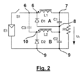
Fig. 2 depicts an embodiment of the buck converter 5. The circuitry includes a
semiconductor switch S1, which can either be an IGBT or a MOSFET with a
voltage rating of
1200 V. A maximum switch voltage will only be present when the switch S1 is
open.
The circuitry also has two choke coils as inductors L1 and L2, which are
magnetically
coupled here, two series capacitors C1 and C2, two freewheeling diodes D1 and
D3, and a
coupling capacitor C3. The load formed by the DC/AC converter 4 is represented
by a
resistor R1. There are five junction points referred to as 6 to 10. The first
junction point 6 is
CA 02780042 2012-05-04
WO 2011/054962 PCT/EP2010/067078
-10-
located between the switch S1 and the inductor L1 / coupling capacitor C3. The
second
junction point 7 is located between the inductor L1 and the first capacitor
C1. The third
junction point 8 is located between the two series capacitors / DC voltage
link capacitors C1
and C2 and between the first diode D1 and the second inductor L2. The fourth
junction point
9 is located between the second series capacitor C2 and the second diode D2.
The fifth
junction point 10 is located between the coupling capacitor C3 and the second
inductor L2 or
the second diode D2, respectively.
The first inductor L1, the first diode D1 and the first capacitor C1 form a
first
subcircuit A; and the second inductor L2, the second diode D2 and the second
capacitor C2
form a second subcircuit B of the buck converter 5. As a result of this, an
output DC voltage
link of the buck converter is split over multiple subcircuits each including
one of the series
capacitors. In addition, two freewheeling paths are formed (L1, D1; L2, D2).
As shown in Fig. 2, the coupling capacitor C3 is connected between first
junction
point 6 and the fifth junction point 10. As indicated by a dotted line, the
coupling capacitor C3
may also be excluded in this variant, in which the inductors L1 and L2 are
magnetically
coupled.
As an alternative to the circuit in Fig. 2, the inductors L1 and L2 can be
formed as
magnetically uncoupled chokes and may be implemented as air coils as shown in
Fig. 3. In
all other respects the circuit has the same configuration as the circuit shown
in Fig. 2.
Ideally, the circuit would operate under continuous current conditions.
Achieving this
preferred condition depends on whether enough energy storage is available, and
not so
much on the specific properties of the components used. As a boundary
condition in a
stationary mode, the voltages across all capacitors are equal to half the
output voltage,
wherein the capacitance of the capacitors C1 and C2 is assumed to be equal,
thereby
enabling the simultaneous blocking of diodes D1 and D2. It would be
advantageous,
CA 02780042 2012-05-04
WO 2011/054962 PCT/EP2010/067078
-11-
however, if capacitor C1 had a much smaller capacitance than capacitor C2 due
to its lower
ripple compared to capacitor C2.
In a first step shown in Fig. 4, the switch S1 is closed. The photovoltaic
input current
is distributed between the two power circuits or subcircuits A and B. One
portion of the
current flows through the first coil or inductor L1 and the load (resistor
R1), while the other
flows through the coupling capacitor C3, the inductor L2 and the capacitor C2.
During this
process the diodes D1 and D2 are blocking, and energy is stored in the chokes
or inductors
L1 and L2 and the capacitors C2 and C3. The current flowing through capacitor
C1 is
negligible, but the capacitor C1 provides for a symmetric distribution of the
output DC link
voltage over the subcircuits A and B. The distribution of the current over the
inductors L1
and L2 and over the capacitors C1, C2, C3, however, is asymmetrical as a
result.
In a second step shown in Fig. 5, the switch S1 is open. The polarity of the
voltage
across both choke coils (inductors L1 and L2) changes, which causes the diodes
D1 and D2
to switch. The load current IR1 is now distributed via the capacitor C2 and
the diode D2. This
causes the two chokes (inductors L1 and L2) and the capacitors C2 and C3 to
discharge. A
switch voltage not exceeding U1-UR1/2 and U1-Uc3 (UR1 being the output voltage
across R1,
and Uc3 being the voltage across capacitor C3) is present at switch S1 at this
moment (i.e.,
approx. 1200 V - 300 V = 900 V). This voltage is significantly lower than both
the input
voltage U1 and the switch voltage rating of 1200 V.
The above steps also require that the capacitors C2 and C3 have the same
capacitance. The voltage ripple on both capacitors therefore has the same
value, which in
turn causes the simultaneous blocking of the diodes D1 and D2.
Fig. 6 shows current waves in normal operation. If S1 is closed (VgateS1 =
high), then
IR1 is roughly equal to IL1, and IC2 is roughly equal to IC3. If switch S1 is
open, then the current
ID1 is roughly equal to ID2, and the direction of the currents IC2 and IC3 is
reversed. Fig. 6 also
CA 02780042 2012-05-04
WO 2011/054962 PCT/EP2010/067078
-12-
shows the currents IL2, Is, and Ic,.
The transformation ratio is determined by the time-integral of the choke
voltage:
JUL,dt = (El - UR1) = ton = (UR1/2) = (T - ton)
From this equation, the following is derived for the voltage transformation
ratio M:
D = (El - UR1) _ (UR1/2) = (1 - D)
UR1/(E1 - UR1) _ (2 = D)/ (1 - D)
M = UR1/E1 = (2 = D) / (1 + D)
wherein
El or U, refers to the photovoltaic voltage or input voltage, and
D refers to the duty cycle.
Conversely, the following applies to the duty cycle D:
D = M/(2 - M)
Fig. 7 shows the relative reverse voltage (Us,max) or the normalized switch
voltage of
the switch S1 as a function of M.
The maximum and periodic switch voltage Us, and the respective diode voltages
Upland UD2 are
Us = UD1 = UD2 = El - (UR1/2) = El = (1 - M/2)
and are therefore dependent on the voltage transformation M.
For this reason, the circuit configuration is only effective for applications
in which the
transformation ratio or input voltage is limited to a specific range, as it is
the case with
photovoltaic applications.
Now, semiconductor losses will be analyzed and then compared to a standard
buck
converter.
To analyze the switching losses in the topology, the amount of DC power that
is
released will be considered first.
CA 02780042 2012-05-04
WO 2011/054962 PCT/EP2010/067078
-13-
PDC2 = IR1 = UR1 = IR1 = El = M
Thus, the amount of DC power that is received is:
PDC1 = Is = El = D = Is I. El = (M/(2 - M)) = PDC2 = IR1 = El = M
The switching current Is is therefore obtained as
IS=IR1=(2-M)
The switching losses are proportional to
Psw = Is = Us E (Us,max) = [IR1 (2 - M)] = [El = (1 - (M/2))] (1 - (Mmin/2))
Psw = IR1 E1 [((2 - M)2 = (2 - Mmin)) / 4]
This results in weighted switching losses normalized to the DC power of
IIS = Psw / PDC _ ((2 - M)2 = (2 - Mmin)) / 4M
Of particular interest in this analysis is the extent to which the switching
losses in the
proposed circuit are changed when compared to a conventional buck converter
given the
same transformation ratio. This leads to:
IIS / Its buck = ((2 - M)2 = (2 - Mmin)) / 4M
Fig. 8 shows the switching losses in normalized form based on the assumption
that
an operation range with a lower limit Mmin allows for the use of switches of
lower voltage
rating having lower specific switching losses.
The average of the squared current curve (Root Mean Square) is used to
illustrate
the conduction losses.
12S,RMS=125= D=[IR1= (2-M)]2= D
With reference to the DC current IR1, the conduction losses of the switch S
yield:
PF / PF(D=1;Mmin=O) = [RS = (IR1 = (2 - M) )2 / (12R1 = Rs)] * D = S(Mmin)
= (2 - M)2 = (M / (2 - M)) = (1 - (Mmin/2))
PF / PF(D=1;Mmin=O) = M = (2 - M) = ((2 - Mmin) / 2)
CA 02780042 2012-05-04
WO 2011/054962 PCT/EP2010/067078
-14-
One interesting aspect of this analysis involves drawing a comparison with a
conventional buck converter. This can be described analytically based on a
simple buck
converter model:
PF / PF(D=1;Mmin=O) = (PF(D=1;Mmin=0) / PF buck) = ((2 - Mmin) / 2). (2 - M)
Fig. 9 shows the normalized conduction losses of the switch S1 as a function
of the
voltage transformation ratio M and the operation range lower limit Mmin.
Both graphics show that the proposed circuitry is characterized by minor
switching
and conduction losses, if the transformation ratio is limited, which is
significantly more
advantageous.
It can therefore be concluded that the circuit configuration based on this
invention
represents the most efficient solution with the lowest number of components.
It is important to note here that a system voltage of approx. 1500 V leads to
the
following voltages:
Maximum photovoltaic voltage (open circuit) : 1500 V
Maximum operating voltage in MPP operation: 1200 V
Maximum switch voltage in MPP operation: approx. 600 V
Because the maximum switch voltage in MPP operation is 600 V only,
semiconductors rated at 1200 V can be used instead of 1700 V rated
semiconductors.
The operating voltage is relevant for selecting the appropriate voltage
rating. The
switch voltage should however not exceed around 2/3 of the maximum operating
voltage
due to the so-called "derating factor", and due to cosmic radiation,
respectively.
Fig. 10 shows a different solution based on prior art that requires a higher
number of
components (as documented in DE 10 2005 047 373 Al). When comparing the
circuits
based on Fig. 2 and Fig. 10, this advantage becomes especially apparent.
The invention is not limited to this example, which means the circuit may also
have
CA 02780042 2012-05-04
WO 2011/054962 PCT/EP2010/067078
-15-
multiple switches S1 in series and/or freewheeling diodes in series to
increase overall
voltage stability. A separation into other subcircuits is also possible.
Another possibility
would involve segmented MPP control of a photovoltaic field through multiple
parallel-
connected input stages or the buck converter 5, respectively.
The DC/AC converter 4 of Fig. 1 may also be based on a configuration that
includes
a DC/DC stage and a DC/AC stage.
Many variations and modifications may be made to the preferred embodiments of
the
invention without departing substantially from the spirit and principles of
the invention. All
such modifications and variations are intended to be included herein within
the scope of the
present invention, as defined by the following claims.
CA 02780042 2012-05-04
WO 2011/054962 PCT/EP2010/067078
-16-
List of Reference Numerals
1 - Inverter
2 - DC input
3 - AC output
4 - DC-AC converter
5 - Buck converter
6 - First junction point
7 - Second junction point
8 - Third junction point
9 - Fourth junction point
10 - Fifth junction point
A - First subcircuit
B - Second subcircuit
N - AC Power grid
PG - Photovoltaic generator
S1 - Semiconductor switch
T - Transformer
D1, D2- Diodes
L1, L2 - Inductors
C1-C3 - Capacitors