Note: Descriptions are shown in the official language in which they were submitted.
CA 02780317 2012-05-07
WO 2011/063216
PCT/US2010/057398
ENCODED CONSUMABLE MATERIALS AND SENSOR ASSEMBLIES FOR USE
IN ADDITIVE MANUFACTURING SYSTEMS
BACKGROUND
The present disclosure relates to direct digital or additive manufacturing
systems for building three-dimensional (3D) models. In particular, the present
disclosure
relates to consumable materials, such as modeling and support materials, for
use in additive
manufacturing systems, such as extrusion-based additive manufacturing systems,
and to
sensors for use with the consumable materials.
An extrusion-based, direct digital or additive manufacturing system (e.g.,
fused deposition modeling systems developed by Stratasys, Inc., Eden Prairie,
MN) is used
to build a 3D model from a digital representation of the 3D model in a layer-
by-layer
manner by extruding a flowable consumable modeling material. The modeling
material is
extruded through an extrusion tip carried by an extrusion head, and is
deposited as a
sequence of roads on a substrate in an x-y plane. The extruded modeling
material fuses to
previously deposited modeling material, and solidifies upon a drop in
temperature. The
position of the extrusion head relative to the substrate is then incremented
along a z-axis
(perpendicular to the x-y plane), and the process is then repeated to form a
3D model
resembling the digital representation.
Movement of the extrusion head with respect to the substrate is performed
under computer control, in accordance with build data that represents the 3D
model. The
build data is obtained by initially slicing the digital representation of the
3D model into
multiple horizontally sliced layers. Then, for each sliced layer, the host
computer generates
a build path for depositing roads of modeling material to form the 3D model.
In fabricating 3D models by depositing layers of a modeling material,
supporting layers or structures are typically built underneath overhanging
portions or in
cavities of objects under construction, which are not supported by the
modeling material
itself. A support structure may be built utilizing the same deposition
techniques by which
the modeling material is deposited. The host computer generates additional
geometry acting
as a support structure for the overhanging or free-space segments of the 3D
model being
formed. Consumable support material is then deposited from a second nozzle
pursuant to
the generated geometry during the build process. The support material adheres
to the
modeling material during fabrication, and is removable from the completed 3D
model when
the build process is complete.
1
CA 02780317 2012-05-07
WO 2011/063216
PCT/US2010/057398
SUMMARY
An aspect of the present disclosure is directed to a marked consumable
material for use in an additive manufacturing system. The marked consumable
material
includes an exterior surface and encoded markings at the exterior surface,
where the
encoded markings are configured to be read by at least one optical sensor
configured to be
operated by the additive manufacturing system. The marked consumable material
is
configured to be consumed in the additive manufacturing system to build at
least a portion
of a three-dimensional model.
Another aspect of the present disclosure is directed to a spooled container
for
providing a marked filament of a material to an additive manufacturing system.
The
spooled container includes a container housing having an exit port, and a
spool retained in
the container housing, where the spool is configured to retain a supply of the
marked
filament. The marked filament has an exterior surface and encoded markings at
the exterior
surface, where the encoded markings extend along at least a portion of a
longitudinal length
of the marked filament. The spooled container also includes an optical sensor
assembly
retained at least partially within the container housing at a location that is
upstream from the
exit port of the container housing. The optical sensor is configured to read
information
from the encoded markings from the marked filament.
Another aspect of the present disclosure is directed to a method for building
a three-dimensional model with an additive manufacturing system. The method
includes
loading a spooled container to the additive manufacturing system, where the
spooled
container has a marked filament that includes an exterior surface having
encoded markings.
At least a portion of the encoded markings have indices of refraction that are
different from
an average index of refraction of the exterior surface. The method also
includes feeding the
marked filament to an optical sensor assembly disposed at least partially
within the spooled
container, reading information from the encoded markings of the fed marked
filament with
the optical sensor assembly, transmitting the read information to the additive
manufacturing
system, and directing the fed marked filament out of the spooled contained and
to a
deposition head of the additive manufacturing system.
BRIEF DESCRIPTION OF THE DRAWINGS
FIG. 1 is a front view of an extrusion-based additive manufacturing system
for building 3D models and support structures from marked consumable materials
having
encoded markings.
2
CA 02780317 2012-05-07
WO 2011/063216
PCT/US2010/057398
FIG. 1A is a front view of an alternative extrusion-based additive
manufacturing system for building 3D models and support structures from marked
consumable materials having encoded markings, which includes sensor assemblies
retained
along consumable material pathways of the system.
FIG. 2 is a perspective view of a segment of a marked cylindrical filament,
which is an example of a marked consumable material for use in the extrusion-
based
additive manufacturing systems.
FIG. 3 is a perspective view of a segment of a marked non-cylindrical
filament, which is an additional example of a marked consumable material for
use in the
extrusion-based additive manufacturing systems.
FIG. 4 is a perspective view of a marked slug or wafer, which is an
additional example of a marked consumable material for use in the extrusion-
based additive
manufacturing systems.
FIG. 5 is a flow diagram of a method for manufacturing marked consumable
materials.
FIG. 6 is a schematic illustration of a laser marking system configured to
form encoded markings in consumable materials.
FIG. 7 is a schematic illustration of a sensor assembly of one embodiment of
the present disclosure in use with a spooled container, where the sensor
assembly contains a
first subassembly located within an extrusion-based additive manufacturing
system and a
second subassembly located within a spooled container.
FIG. 8 is an expanded view of the sensor assembly shown in FIG. 7.
FIG. 9 is a bottom perspective view of the sensor assembly.
FIG. 10 is an exploded perspective view of the first subassembly of the
sensor assembly.
FIG. 11 is a perspective view of the second subassembly of the sensor
assembly.
FIG. 12 is a bottom view of the sensor assembly, illustrating an engagement
and operation of the first and second subassemblies.
FIG. 13 is a schematic illustration of a sensor assembly of a second
embodiment of the present disclosure in use with a spooled container.
3
CA 02780317 2012-05-07
WO 2011/063216
PCT/US2010/057398
FIG. 14 is an expanded schematic illustration of an example of the second
embodied sensor assembly in use with a marked consumable material, where the
shown
sensor assembly is configured to detect far-field diffraction patterns.
DETAILED DESCRIPTION
The present disclosure is directed to marked consumable materials for use in
additive manufacturing systems (also referred to as direct digital
manufacturing systems),
such as extrusion-based digital manufacturing systems. The marked consumable
materials
include encoded markings that may contain a variety of information, such as
information
relating to properties of the marked consumable materials (e.g., physical and
compositional
properties) and information relating to parameters for operating the additive
manufacturing
systems (e.g., extrusion parameters).
The present disclosure is also directed sensor assemblies configured to read
the encoded markings from successive portions of the marked consumable
materials as the
marked consumable materials are fed to the additive manufacturing systems. As
discussed
below, the sensor assemblies may transmit the information read from the
encoded markings
to one or more control components of the additive manufacturing systems. This
allows the
additive manufacturing systems to use the information in the encoded markings
for a variety
of different purposes, such as for building 3D models and/or support
structures.
FIG. 1 is a front view of system 10, which is an additive or direct digital
manufacturing system, such as an extrusion-based additive manufacturing
system. Suitable
extrusion-based additive manufacturing systems for system 10 include fused
deposition
modeling systems developed by Stratasys, Inc., Eden Prairie, MN. As shown,
system 10
includes build chamber 12, platen 14, gantry 16, extrusion head 18, supply
sources 20 and
22, and sensor assemblies 24 and 26, where sensor assemblies 24 and 26 are
configured to
read information from marked consumable materials (not shown in FIG. 1)
provided in
supply sources 20 and 22.
Build chamber 12 is an enclosed environment that contains platen 14, gantry
16, and extrusion head 18 for building a 3D model (referred to as 3D model 28)
and a
corresponding support structure (referred to as support structure 30). Build
chamber 12 is
desirably heated to reduce the rate at which the modeling and support
materials solidify
after being extruded and deposited.
Platen 14 is a platform on which 3D model 28 and support structure 30 are
built, and moves along a vertical z-axis based on signals provided from a
computer-operated
4
CA 02780317 2015-01-12
controller (referred to as controller 32). As shown, controller 32 may
communicate with
build chamber 12, platen 14, gantry 16, and extrusion head 18 over
communication line 34.
While illustrated as a single signal line, communication line 34 may include
one or more
signal lines for allowing controller 32 to communicate with various components
of system
10, such as build chamber 12, platen 14, gantry 16, and extrusion head 18.
Gantry 16 is a guide rail system configured to move extrusion head 18 in a
horizontal x-y plane within build chamber 12 based on signals provided from
controller 32
(via communication line 34). The horizontal x-y plane is a plane defined by an
x-axis and a
y-axis (not shown in FIG. 1), where the x-axis, the y-axis, and the z-axis are
orthogonal to
each other. In an alternative embodiment, platen 14 may be configured to move
in the
horizontal x-y plane within build chamber 12, and extrusion head 18 may be
configured to
move along the z-axis. Other similar arrangements may also be used such that
one or both
of platen 14 and extrusion head 18 are moveable relative to each other.
Extrusion head 18 is supported by gantry 16 for building 3D model 28 and
support structure 30 on platen 14 in a layer-by-layer manner, based on signals
provided
from controller 32. Extrusion head 18 includes a pair of liquefiers (not shown
in FIG. 1)
configured to receive and melt successive portions of the marked consumable
materials.
Examples of suitable extrusion heads for extrusion head 18 include those
disclosed in
LaBossiere, et al., U.S. Patent Application Publication Nos. 2007/0003656 and
2007/00228590; Leavitt, U.S. Patent Application Publication No. 2009/0035405;
and
Batchelder et al., U.S. Patent Nos. 8,439,665; 8,221,669; and 8,236,227.
Alternatively,
system 10 may include one or more two-stage pump assemblies, such as those
disclosed in
Batchelder et al., U.S. Patent No. 5,764,521; and Skubic et al., U.S. Patent
Application
Publication No. 2008/0213419. Furthermore, system 10 may include a plurality
of
extrusion heads 18 for depositing modeling and/or support materials.
Supply sources 20 and 22 are devices configured to retain supplies of the
marked consumable materials, and may be respectively loaded into bays 20a and
22a of
system 10. In the shown embodiment, supply source 20 retains a supply of a
marked
modeling material and supply source 22 retains a supply of a marked support
material.
System 10 may also include additional drive mechanisms (not shown) configured
to assist
in feeding the marked consumable materials from supply sources 20 and 22 to
extrusion
head 18.
CA 02780317 2015-01-12
In some embodiments, the marked consumable materials may be provided to
system 10 as filaments having marked exterior surfaces (not shown in FIG. 1),
such as
marked cylindrical filaments and/or marked non-cylindrical filaments, as
discussed below.
In these embodiments, suitable assemblies (e.g., spooled containers) for
supply sources 20
and 22 include those disclosed in Swanson et al., U.S. Patent No. 6,923,634;
Comb et al.,
U.S. Patent No. 7,122,246; Taatjes et al, U.S. Patent Application Publication
Nos.
2010/0096485 and 2010/0096489; and Swanson, U.S. Patent No. 8,403,658 and
International PCT Publication No. W02009/088995.
In alternative embodiments, the marked consumable materials may be
provided to system 10 as marked slugs or wafers, as discussed below. In these
embodiments, suitable assemblies for supply sources 20 and 22 include those
disclosed in
Batchelder et al., U.S. Patent No. 5,764,521.
Sensor assemblies 24 and 26 are configured to read the encoded markings of
the marked consumable materials as the marked consumable materials are fed to
extrusion
head 18. Sensor assembly 24 may be retained at any suitable location between
(or within)
supply source 20 and extrusion head 18. Similarly, sensor assembly 26 may be
retained at
any suitable location between (or within) supply source 22 and extrusion head
18. In the
shown example, sensor assemblies 24 and 26 are retained partially or fully
within supply
sources 20 and 22, respectively.
In alternative embodiments, as disclosed in U.S. Patent Application
Publication No. 2011/017268 and shown in FIG. 1A, sensor assemblies 24 and 26
may be
retained along filament pathways within system 10 adjacent to supply sources
20 and 22,
respectively. In further alternative embodiments, one or both of sensor
assemblies 24 and
26 may be retained by gantry 16 with extrusion head 18, thereby moving sensor
assemblies
24 and 26 with extrusion head 18.
As shown in FIG. 1, the marked modeling material may be provided to
extrusion head 18 from supply source 20 through pathway 36, where pathway 36
may
include a guide tube (not shown) for guiding the marked modeling material to
extrusion
head 18. In the shown embodiment, pathway 36 is downstream from sensor
assembly 24,
thereby allowing sensor assembly 24 to read the encoded information from the
marked
modeling material prior to passing through pathway 36. As further shown,
sensor assembly
24 may communicate with controller 32 and/or any other control component of
system 10
(e.g., a host computer system for system 10, not shown) over communication
line 38.
6
CA 02780317 2012-05-07
WO 2011/063216
PCT/US2010/057398
While illustrated as a single signal line, communication line 38 may include
one or more
signal lines for allowing sensor assembly 24 to communicate with one or more
control
components of system 10 (e.g., controller 32).
Similarly, the marked support material may be provided to extrusion head 18
from supply source 22 through pathway 40, where pathway 40 may also include a
guide
tube (not shown) for guiding the marked support material to extrusion head 18.
In the
shown embodiment, pathway 40 is downstream from sensor assembly 26, thereby
allowing
sensor assembly 26 to read the encoded information from the marked support
material prior
to passing through pathway 40. As further shown, sensor assembly 26 may
communicate
with controller 32 and/or any other control component of system 10 (e.g., the
host computer
system for system 10) over communication line 42. While illustrated as a
single signal line,
communication line 42 may include one or more signal lines for allowing sensor
assembly
26 to communicate with one or more control components of system 10 (e.g.,
controller 32).
During a build operation, the marked consumable materials may be fed to
extrusion head 18 through pathways 36 and 40. Sensor assemblies 24 and 26 may
read the
encoded markings of the marked consumable materials as successive portions of
the marked
consumable materials exit supply sources 20 and 22, and enter pathways 36 and
40.
Information retained in the encoded markings may then be transmitted to
controller 32 over
communication lines 38 and 42, thereby allowing controller 32 to use the
received
information to assist in building 3D model 28 and/or support structure 30. For
example,
controller 32 may modify the extrusion parameters transmitted to extrusion
head 18,
allowing the thermal properties of extrusion head 18 to be adjusted based on
the received
information. In one embodiment, the thermal properties of extrusion head 18
may be
adjusted based on received information relating to the cross sectional areas
of successive
portions of the consumable materials.
Additionally, the received information may relate to the amount of the
marked consumable materials remaining in supply source 20 or 22. This is
beneficial for
informing a user of system 10 how long the current supply of the marked
consumable
material will last before the user needs to load a new supply source to system
10. This
information is particularly suitable for allowing the user to know if the
build operation will
end during a time period when the user may not necessarily be present to load
a new supply
source to system 10 (e.g., during overnight and/or weekend periods).
7
CA 02780317 2012-05-07
WO 2011/063216
PCT/US2010/057398
Furthermore, the received information may relate to the marked consumable
material itself, such as the material type (e.g., modeling and support
materials), material
composition, and/or the material color. Sensor assemblies 24 and 26 may read
these types
of information from the marked consumable materials to confirm that the proper
material
was loaded to system 10, thereby reducing the risk of accidentally running
system 10 with
an incorrect material. For example, sensor assembly 24 may read information
from the
marked consumable material being fed from supply source 20, and controller 32
may
confirm that the material being fed through pathway 36 is an intended modeling
material,
rather than a support material.
Combinations of the read information may also be used to assist in building
3D model 28 and/or support structure 30. For example, in embodiments in which
bays 20a
and 22a may each accept supply sources of modeling and support materials, the
user may
load supply source 20 of the marked modeling material into either bay 20a or
bay 22a, and
after the corresponding sensor assembly 24 or 26 reads the information from
the marked
consumable material, controller 32 may identify that the material is a
modeling material for
building 3D model 28 and adjust the extrusion parameters and feed rates
accordingly. A
similar arrangement may be accomplished with the marked support material in
supply
source 22. This prevents the user from having to load a particular supply
source into a
particular bay of system 10.
As the marked consumable materials are fed to extrusion head 18, gantry 16
may move extrusion head 18 around in the horizontal x-y plane within build
chamber 12.
Extrusion head 18 thermally melts the successive portions of the received
marked modeling
material, thereby allowing the molten modeling material to be extruded to
build 3D model
28. Similarly, extrusion head 18 thermally melts the successive portions of
the marked
support material, thereby allowing the molten support material to be extruded
to build
support structure 30. The upstream, unmelted portions of the marked consumable
materials
may each function as a piston with a viscosity-pump action to extrude the
molten material
out of the respective liquefiers of extrusion head 18.
The extruded modeling and support materials are deposited onto platen 14 to
build 3D model 28 and support structure 30 using a layer-based additive
technique. Support
structure 30 is desirably deposited to provide vertical support along the z-
axis for
overhanging regions of the layers of 3D model 28. After the build operation is
complete,
the resulting 3D model 28/support structure 30 may be removed from build
chamber 12, and
8
CA 02780317 2012-05-07
WO 2011/063216
PCT/US2010/057398
support structure 30 may be removed from 3D model 28. As used herein, the term
"three-
dimensional model" is intended to encompass any object built with an additive
manufacturing system, and includes 3D models built from modeling materials
(e.g., 3D
model 28) as well a support structures built from support materials (e.g.,
support structure
30).
FIG. 2 illustrates a segment of filament 44, which is an example of a suitable
marked consumable material of the present disclosure for use as a marked
modeling
material and/or a marked support material with system 10 (shown in FIG. 1). As
shown in
FIG. 2, filament 44 is a marked cylindrical filament having length 46, where
length 46 is a
continuous length that may vary depending on the amount of filament 44
remaining in
supply source 20 or 22. While only a segment of filament 44 is illustrated in
FIG. 2, it is
understood that length 46 of filament 44 may extend for a substantial distance
(e.g., greater
than 25 meters).
Filament 44 also includes exterior surface 48 extending along length 46 and
encoded markings 50, where encoded markings 50 are located at exterior surface
48 along
at least a portion of length 46. In one embodiment, encoded markings 50 extend
substantially along the entire length 46. Filament 44 also has a surface
diameter (referred to
as surface diameter 52) at a non-marked location that is desirably configured
to allow
filament 44 to mate with a liquefier of extrusion head 18 without undue
friction. Examples
of suitable average diameters for surface diameter 52 range from about 0.8
millimeters
(about 0.03 inches) to about 2.5 millimeters (about 0.10 inches), with
particularly suitable
average diameters ranging from about 1.0 millimeter (about 0.04 inches) to
about 2.3
millimeters (about 0.09 inches), and with even more particularly suitable
average diameters
ranging from about 1.3 millimeters (about 0.05 inches) to about 2.0
millimeters (about 0.08
inches).
In the shown embodiment, encoded markings 50 are trench-based markings
in exterior surface 48 (e.g., via laser ablation). However, as discussed
below, encoded
markings 50 may alternatively be form on filament 44 using a variety of
different marking
techniques. For example, encoded markings 50 may be formed as coatings over
exterior
surface 48 via one or more coating processes (e.g., jetting and evaporation
processes).
Alternatively, encoded markings 50 may be formed by cross-linking the surface
material of
filament 44, such as with ultraviolet light, to vary the index of refraction
of the material at
9
CA 02780317 2012-05-07
WO 2011/063216
PCT/US2010/057398
encoded markings 50. This is particularly suitable in embodiments in which
encoded
markings 50 function as diffraction gratings.
Encoded markings 50 include encoded information, which may be read by
sensor assembly 24 or 26 as successive portions of filament 44 pass through
pathway 36 or
40 of system 10. As discussed above, the read information may then be
transmitted to
controller 32 over communication line 38 or 42, thereby allowing controller 32
to use the
received information to assist in building 3D model 28 and/or support
structure 30.
Encoded markings 50 may extend in multiple linear paths along length 46
(referred to as paths 50a and 50b), as shown. In this embodiment, encoded
markings 50
may also include a third linear path (referred to as path 50c, not shown) such
that paths 50a,
50b, and 50c are each separated by angles of about 120 degrees. This
arrangement is
beneficial for allowing sensor assembly 24 or 26 to read at least one of paths
50a, 50b, and
50c regardless of the axial orientation of filament 44 as successive portions
of filament 44
pass through the given sensor assembly 24 or 26. In alternative embodiments,
filament 44
may include fewer or additional paths of encoded markings 50 such that
filament 44
includes at least one path of encoded markings 50 (e.g., paths 50a, 50b, and
50c). In
additional alternative embodiments, one or more of the paths (e.g., paths 50a,
50b, and 50c)
may extend along length 46 in a non-linear manner (e.g., S-curves and spiral
arrangements).
Encoded markings 50 may include a variety of different information, such as
information relating to filament 44 and/or system 10. Examples of suitable
types of
information that may be included in encoded markings 50 include local filament
cross-
sections (e.g., diameters and root-mean-square variations), local and global
filament
extrusion parameters, length of filament 44 remaining in supply source 20 or
22,
measurements of local filament fingerprint characteristics, material type
(e.g., modeling and
support materials), material composition, material color, manufacturing
information for
filament 44 (e.g., manufacturing dates, manufacturing locations, and lot
numbers), product
codes, material origin information, software and firmware updates for system
10, and
combinations thereof.
In addition, encoded markings 50 may also include media-based information,
such as operating and use instructions, artistic works (e.g., textual, video,
and audio
information), and the like. In these embodiments, system 10 may include
capabilities for
playing the encoded media, such as textual and/or graphical information that
may be
displayed for a user of system 10 to read, and/or audio information that may
be played for a
CA 02780317 2012-05-07
WO 2011/063216
PCT/US2010/057398
user of system 10 to hear. The amount of data per unit length along length 46
of filament
44 may vary depending on the particular marking technique used, the encoding
scheme
used, the dimensions of encoded markings 50, the number of encoded markings
per unit
length along length 46, and the like.
The dimensions and geometries of each mark of encoded markings 50 may
vary depending on the encoding scheme and the marking technique used. In the
current
example in which encoded markings 50 are formed as trenches in exterior
surface 48 (e.g.,
via laser ablation), encoded markings 50 desirably have small dimensions
relative to the
overall dimensions of filament 44 to minimize or otherwise reduce their impact
on the
diameter of filament 44. Additionally, as shown in the current embodiment, the
trenches of
encoded markings 50 have axial lengths (e.g., axial length 54) that vary to
provide patterns
based on the encoding scheme used. In alternative embodiments one or more of
the radial
widths of the marks (referred to as widths 56) and/or the depths of the marks
may
additionally or alternatively be varied to provide patterns based on the
encoding scheme
used.
Suitable average dimensions for width 56 range from about 51 micrometers
(about 2 mils) to about 510 micrometers (about 20 mils), with particularly
suitable average
dimensions ranging from about 130 micrometers (about 5 mils) to about 250
micrometers
(about 10 mils). Suitable dimensions for the axial lengths along length 46
(e.g., axial length
54) range from about 130 micrometers (about 5 mils) to about 5,100 micrometers
(about
200 mils), with particularly suitable axial lengths ranging from about 1,300
micrometers
(about 50 mils) to about 3,800 micrometers (about 150 mils).
Furthermore, suitable average depths of each mark of encoded markings 50
from exterior surface 48 range from about 1.3 micrometers (about 0.05 mils) to
about 51
micrometers (about 2 mils), with particularly suitable average depths ranging
from about 13
micrometers (about 0.5 mil) to about 38 micrometers (about 1.5 mils). As
discussed below,
the edges of the trench marks are suitable regions for scattering light in a
darkfield
illumination, which may allow an optical sensor assembly to read encoded
markings 50
based on the patterns of the scattered light. In alternative embodiments, the
encoded
markings of filament 44 may be two-dimensional markings (e.g., coatings)
rather than the
three-dimensional geometry of encoded markings 50.
In further alternative embodiments, the axial lengths (e.g., axial length 54)
and the radial widths (e.g., widths 56) of encoded markings 50 may be the same
or
11
CA 02780317 2012-05-07
WO 2011/063216
PCT/US2010/057398
substantially the same. In these embodiments, the patterns of encoded markings
50 along
length 46 of filament 44 may vary to provide the encoding properties. For
example, in
embodiments in which encoded markings 50 function as diffraction gratings,
encoded
markings 50 may be formed as patterns of parallel lines having different
indices of
refraction from that of exterior surface 48. The parallel lines of encoded
markings 50 may
be the same or similar in geometry. However, the patterns of the parallel
lines and the
interstitial areas of exterior surface 48 may define the encoded pattern in
filament 44.
Filament 44 may be manufactured from a variety of extrudable modeling and
support materials for respectively building 3D model 28 and support structure
30. Suitable
modeling materials for filament 44 include polymeric and metallic materials.
In some
embodiments, suitable modeling materials include materials having amorphous
properties,
such as thermoplastic materials, amorphous metallic materials, and
combinations thereof.
Examples of suitable thermoplastic materials for filament 44 include
acrylonitrile-
butadiene-styrene (ABS) copolymers, polycarbonates, polysulfones,
polyethersulfones,
polyphenylsulfones, polyetherimides, amorphous polyamides, modified variations
thereof
(e.g., ABS-M30 copolymers), polystyrene, and blends thereof. Examples of
suitable
amorphous metallic materials include those disclosed in Batchelder, U.S.
Patent Application
Publication No. 2009/0263582.
Suitable support materials for filament 44 include polymeric materials. In
some embodiments, suitable support materials include materials having
amorphous
properties (e.g., thermoplastic materials) and that are desirably removable
from the
corresponding modeling materials after 3D model 28 and support structure 30
are built.
Examples of suitable support materials for filament 44 include water-soluble
support
materials commercially available under the trade designations "SR10", "5R20",
and
"5R30" Soluble Supports from Stratasys, Inc., Eden Prairie, MN; break-away
support
materials commercially available under the trade designation "BASS" from
Stratasys, Inc.,
Eden Prairie, MN, and those disclosed in Crump et al., U.S. Patent No.
5,503,785;
Lombardi et al., U.S. Patent Nos. 6,070,107 and 6,228,923; Priedeman et al.,
U.S. Patent
No. 6,790,403; and Hopkins et al., U.S. Patent Application Publication No.
2010/0096072.
The composition of filament 44 may also include additional additives, such
as plasticizers, rheology modifiers, inert fillers, colorants, stabilizers,
and combinations
thereof. Examples of suitable additional plasticizers for use in the support
material include
dialkyl phthalates, cycloalkyl phthalates, benzyl and aryl phthalates, alkoxy
phthalates,
12
CA 02780317 2012-05-07
WO 2011/063216
PCT/US2010/057398
alkyl/aryl phosphates, polyglycol esters, adipate esters, citrate esters,
esters of glycerin, and
combinations thereof. Examples of suitable inert fillers include calcium
carbonate,
magnesium carbonate, glass spheres, graphite, carbon black, carbon fiber,
glass fiber, talc,
wollastonite, mica, alumina, silica, kaolin, silicon carbide, composite
materials (e.g.,
spherical and filamentary composite materials), and combinations thereof. In
embodiments
in which the composition includes additional additives, examples of suitable
combined
concentrations of the additional additives in the composition range from about
I% by
weight to about 10% by weight, with particularly suitable concentrations
ranging from
about I% by weight to about 5% by weight, based on the entire weight of the
composition.
Filament 44 also desirably exhibits physical properties that allow filament 44
to be used as a consumable material in system 10. For example, filament 44 is
desirably
flexible along length 46 to allow filament 44 to be retained in supply sources
20 and 22
(e.g., wound on spools) and to be fed through system 10 (e.g., through
pathways 36 and 40)
without plastically deforming or fracturing. For example, in one embodiment,
filament 44
is capable of withstanding elastic strains greater than t/r, where "t" is a
cross-sectional
thickness of filament 44 in the plane of curvature, and "r" is a bend radius
(e.g., a bend
radius in supply source 20 or 22 and/or a bend radius through pathway 36 or
40).
In one embodiment, the composition of filament 44 is substantially
homogenous along length 46. Additionally, the composition of filament 44
desirably
exhibits a glass transition temperature that is suitable for use in build
chamber 12.
Examples of suitable glass transition temperatures at atmospheric pressure for
the
composition of filament 44 include temperatures of about 80 C or greater. In
some
embodiments, suitable glass transition temperatures include about 100 C or
greater. In
additional embodiments, suitable glass transition temperatures include about
120 C or
greater.
Filament 44 also desirably exhibits low compressibility such that its axial
compression doesn't cause filament 44 to be seized within a liquefier.
Examples of suitable
Young's modulus values for the polymeric compositions of filament 44 include
modulus
values of about 0.2 gigapascals (GPa) (about 30,000 pounds-per-square inch
(psi)) or
greater, where the Young's modulus values are measured pursuant to ASTM D638-
08. In
some embodiments, suitable Young's modulus range from about 1.0 GPa (about
145,000
psi) to about 5.0 GPa (about 725,000 psi). In additional embodiments, suitable
Young's
13
CA 02780317 2012-05-07
WO 2011/063216
PCT/US2010/057398
modulus values range from about 1.5 GPa (about 200,000 psi) to about 3.0 GPa
(about
440,000 psi).
FIG. 3 illustrates a segment of filament 58, which is an additional example of
a suitable marked consumable material of the present disclosure for use as a
modeling
material and/or a support material with system 10 (shown in FIG. 1). As shown
in FIG. 3,
filament 58 is a marked non-cylindrical filament having length 60, where
length 60 is a
continuous length that may vary depending on the amount of filament 58
remaining in
supply source 20 or 22. While only a segment of filament 58 is illustrated in
FIG. 3, it is
understood that length 60 of filament 58 may extend for a substantial distance
(e.g., greater
than 25 meters).
Filament 58 also includes exterior surface 62 extending along length 60 and
having major surfaces 64 and 66, which are the opposing major surfaces of
filament 58.
Filament 58 further includes encoded markings 68 located at major surface 64
of exterior
surface 62, along at least a portion of length 60. In one embodiment, encoded
markings 68
extend substantially along the entire length 60.
In the shown embodiment, encoded markings 68 are trench-based markings
in exterior surface 62 (e.g., via laser ablation), as discussed above for
encoded markings 50
of filament 44 (shown in FIG. 2). However, as discussed below, encoded
markings 68 may
alternatively be formed on filament 58 using a variety of different marking
techniques (e.g.,
via one or more coating processes). For example, encoded markings 68 may be
formed by
cross-linking the surface material of filament 58, such as with ultraviolet
light, to vary the
index of refraction of the material at encoded markings 68. This is
particularly suitable in
embodiments in which encoded markings 68 function as diffraction gratings.
Encoded markings 68 may extend in a single linear path along length 60 at
major surface 64, as shown. In comparison to filament 44, which has a
cylindrical cross
section, filament 58 is less susceptible to axial rotation due to its
rectangular cross section.
As such, so long as filament 58 is provided to system 10 in the proper
orientation, sensor
assembly 24 or 26 may read encoded markings 68 as successive portions of
filament 58 pass
through the given sensor assembly 24 or 26. In an alternative embodiment,
encoded
markings 50 may also include an additional linear path along length 60 at
major surface 66,
and/or along the edges of filament 58. This embodiment allows sensor assembly
24 or 26 to
read encoded markings 68 regardless of the orientation of filament 58. In
additional
alternative embodiments, filament 58 may include additional paths of encoded
markings 68
14
CA 02780317 2015-01-12
at one or both of major surfaces 64 and 66. Furthermore, one or more of the
paths of
encoded markings 68 may extend along length 60 in a non-linear manner (e.g., S-
curves
and spiral arrangements).
Encoded markings 68 may include a variety of different information, such as
information relating to filament 58 and/or system 10, which may be read by
sensor
assembly 24 or 26 in the same manner as discussed above for encoded markings
50 of
filament 44. Accordingly, suitable types of information that may be retained
in encoded
markings 68 include those discussed above for encoded markings 50.
Filament 58 has a cross section defined by width 70 and thickness 72, thereby
defining a non-cylindrical cross section. Examples of suitable non-cylindrical
filaments for
filament 58 include those disclosed in Batchelder et al., U.S. Patent Nos.
8,439,665;
8,221,669; and 8,236,227. Filament 58 is also desirably flexible along length
60 to allow
filament 58 to be retained in supply sources 20 and 22 (e.g., wound on spools)
and to be fed
through system 10 (e.g., through pathways 36 and 40) without plastically
deforming or
fracturing. For example, in one embodiment, filament 58 is capable of
withstanding elastic
strains greater than t/r, where "t" is a cross-sectional thickness of filament
58 in the plane
of curvature, and "r" is a bend radius (e.g., a bend radius in supply source
20 or 22 and/or a
bend radius through pathway 36 or 40).
Examples of suitable average dimensions for width 70 range from about 1.0
millimeter (about 0.04 inches) to about 10.2 millimeters (about 0.40 inches),
with
particularly suitable average widths ranging from about 2.5 millimeters (about
0.10 inches)
to about 7.6 millimeters (about 0.30 inches), and with even more particularly
suitable
average widths ranging from about 3.0 millimeters (about 0.12 inches) to about
5.1
millimeters (about 0.20 inches).
Examples of suitable average dimensions for thickness 72 range from about
0.08 millimeters (about 0.003 inches) to about 1.5 millimeters (about 0.06
inches), with
particularly suitable average thicknesses ranging from about 0.38 millimeters
(about 0.015
inches) to about 1.3 millimeters (about 0.05 inches), and with even more
particularly
suitable average thicknesses ranging from about 0.51 millimeters (about 0.02
inches) to
about 1.0 millimeter (about 0.04 inches).
Examples of suitable aspect ratios of width 70 to thickness 72 include aspect
ratios greater than about 2:1, with particularly suitable aspect ratios
ranging from about
CA 02780317 2012-05-07
WO 2011/063216
PCT/US2010/057398
2.5:1 to about 20:1, and with even more particularly suitable aspect ratios
ranging from
about 3:1 to about 10:1.
The dimensions and geometries of each mark of encoded markings 68 may
also vary depending on the encoding scheme and the marking technique used. In
the
current example in which encoded markings 68 are formed as trenches in
exterior surface
62 (e.g., via laser ablation), encoded markings 68 desirably have small
dimensions relative
to the overall dimensions of filament 58 to minimize or otherwise reduce their
impact on the
cross sectional area of filament 58. Additionally, as shown in the current
embodiment, the
trenches of encoded markings 68 have axial lengths (along length 60) that vary
to provide
patterns based on the encoding scheme used. In alternative embodiments one or
more of the
widths of the marks (along width 70) and/or the depths of the marks (along
thickness 72)
may additionally or alternatively be varied to provide patterns based on the
encoding
scheme used. Examples of suitable axial lengths, widths, and depths for each
mark of
encoded markings 68 include those discussed above for encoded markings 50 of
filament
44.
Furthermore, the axial lengths along length 60 and the widths along widths
70 of encoded markings 68 may be the same or substantially the same. In these
embodiments, the patterns of encoded markings 68 along length 60 of filament
58 may vary
to provide the encoding properties. For example, in embodiments in which
encoded
markings 68 function as diffraction gratings, encoded markings 68 may be
formed as
patterns of parallel lines having different indices of refraction from that of
major surface 64
and/or major surface 66. The parallel lines of encoded markings 68 may be the
same or
similar in geometry. However, the patterns of the parallel lines and the
interstitial areas of
major surface 64 and/or major surface 66 may define the encoded pattern in
filament 58.
Filament 58 may also be manufactured from a variety of extrudable
modeling and support materials for respectively building 3D model 28 and
support structure
30. Examples of suitable modeling and support materials include those
discussed above for
filament 44. Filament 58 also desirably exhibits physical properties that
allow filament 58
to be used as a consumable material in system 10. In one embodiment, the
composition of
filament 58 is substantially homogenous along length 60. Additionally, the
composition of
filament 58 desirably exhibits a glass transition temperature that is suitable
for use in build
chamber 12. Examples of suitable glass transition temperatures at atmospheric
pressure for
the composition of filament 58 include those discussed above for filament 44.
Filament 58
16
CA 02780317 2012-05-07
WO 2011/063216
PCT/US2010/057398
also desirably exhibits low compressibility such that its axial compression
doesn't cause
filament 58 to be seized within a liquefier. Examples of suitable Young's
modulus values
for the polymeric compositions of filament 58 include those discussed above
for filament
44.
FIG. 4 illustrates slug or wafer 74, which is an additional example of a
suitable marked consumable material of the present disclosure for use as a
modeling
material and/or a support material with system 10 (shown in FIG. 1). As shown
in FIG. 4,
slug 74 dimensionally includes length 76, width 78, and thickness 80. Examples
of suitable
designs for slug 74 include those disclosed in Batchelder et al., U.S. Patent
No. 5,764,521.
Accordingly, a series of slugs 74 may be fed through pathway 36 or 40 in an
end-to-end
arrangement to provide slugs 74 to extrusion head 18.
Slug 74 also includes exterior surface 82 extending along length 76, and
encoded markings 84 located at exterior surface 82, along at least a portion
of length 76. In
one embodiment, encoded markings 84 extend substantially along the entire
length 86. In
the shown embodiment, encoded markings 84 are trench-based markings in
exterior surface
82 (e.g., via laser ablation), as discussed above for encoded markings 50 of
filament 44
(shown in FIG. 2). However, as discussed below, encoded markings 84 may
alternatively
be written to slug 74 using a variety of different marking techniques (e.g.,
via one or more
coating processes). For example, encoded markings 84 may be formed by cross-
linking the
surface material of slug 74, such as with ultraviolet light, to vary the index
of refraction of
the material at encoded markings 84. This is particularly suitable in
embodiments in which
encoded markings 84 function as diffraction gratings.
Encoded markings 84 may extend in a single linear path along length 76 at
one or both major surfaces of exterior surface 82, as shown. In additional
alternative
embodiments, slug 74 may include additional paths of encoded markings 84 at
one or both
of major surfaces of exterior surface 82. Furthermore, one or more of the
paths of encoded
markings 84 may extend along length 76 in a non-linear manner (e.g., S-curves
and spiral
arrangements).
Encoded markings 84 may also include a variety of different information,
such as information relating to slug 74 and/or system 10, which may be read by
sensor
assembly 24 or 26 in the same manner as discussed above for encoded markings
50 of
filament 44. Accordingly, suitable types of information that may be retained
in encoded
markings 84 include those discussed above for encoded markings 50.
17
CA 02780317 2012-05-07
WO 2011/063216
PCT/US2010/057398
Examples of suitable average dimensions for length 76 range from about 25
millimeters (about 1.0 inch) to about 150 millimeters (about 6.0 inches), with
particularly
suitable average lengths ranging from about 38 millimeters (about 1.5 inches)
to about 76
millimeters (about 3.0 inches), and with even more particularly suitable
average lengths
ranging from about 43 millimeters (about 1.7 inches) to about 64 millimeters
(about 2.5
inches).
Examples of suitable average dimensions for width 78 range from about 10
millimeters (about 0.4 inches) to about 38 millimeters (about 1.5 inches),
with particularly
suitable average widths ranging from about 13 millimeters (about 0.5 inches)
to about 33
millimeters (about 1.3 inches), and with even more particularly suitable
average widths
ranging from about 15 millimeters (about 0.6 inches) to about 25 millimeters
(about 1.0
inch).
Examples of suitable average dimensions for thickness 80 range from about
1.3 millimeters (about 0.05 inches) to about 13 millimeters (about 0.5
inches), with
particularly suitable average thicknesses ranging from about 2.5 millimeters
(about 0.1
inches) to about 7.6 millimeters (about 0.3 inches), and with even more
particularly suitable
average thicknesses ranging from about 3.8 millimeters (about 0.15 inches) to
about 6.4
millimeters (about 0.25 inches).
The dimensions and geometries of each mark of encoded markings 84 may
also vary depending on the encoding scheme and the marking technique used. In
the
current example in which encoded markings 84 are formed as trenches in
exterior surface
82 (e.g., via laser ablation), encoded markings 84 desirably have small
dimensions relative
to the overall dimensions of slug 74 to minimize or otherwise reduce their
impact on the
cross sectional area of slug 74. Additionally, as shown in the current
embodiment, the
trenches of encoded markings 84 have axial lengths (along length 76) that vary
to provide
patterns based on the encoding scheme used. In alternative embodiments one or
more of the
widths of the marks (along width 78) and/or the depths of the marks (along
thickness 80)
may additionally or alternatively be varied to provide patterns based on the
encoding
scheme used. Examples of suitable axial lengths, widths, and depths for each
mark of
encoded markings 84 include those discussed above for encoded markings 50 of
filament
44.
Furthermore, the axial lengths and the widths of encoded markings 84 may
be the same or substantially the same. In these embodiments, the patterns of
encoded
18
CA 02780317 2012-05-07
WO 2011/063216
PCT/US2010/057398
markings 84 along the length of slug 74 may vary to provide the encoding
properties. For
example, in embodiments in which encoded markings 84 function as diffraction
gratings,
encoded markings 84 may be formed as patterns of parallel lines having
different indices of
refraction from that of exterior surface 82. The parallel lines of encoded
markings 84 may
be the same or similar in geometry. However, the patterns of the parallel
lines and the
interstitial areas of exterior surface 82 may define the encoded pattern in
slug 74.
Slug 74 may also be manufactured from a variety of extrudable modeling
and support materials for respectively building 3D model 28 and support
structure 30.
Examples of suitable modeling and support materials include those discussed
above for
filament 44. Slug 74 also desirably exhibits physical properties that allow
slug 74 to be
used as a consumable material in system 10. In one embodiment, the composition
of slug
74 is substantially homogenous along length 76. Additionally, the composition
of slug 74
desirably exhibits a glass transition temperature that is suitable for use in
build chamber 12.
Examples of suitable glass transition temperatures at atmospheric pressure for
the
composition of slug 74 include those discussed above for filament 44. Slug 74
also
desirably exhibits low compressibility such that its axial compression doesn't
cause slug 74
to be seized within a liquefier. Examples of suitable Young's modulus values
for the
polymeric compositions of slug 74 include those discussed above for filament
44.
In addition to the above-discussed marked consumable material geometries,
the marked consumable materials of the present disclosure include a variety of
geometries,
such as pellet geometries, irregular geometries, and the like. For example,
the marked
consumable materials may be provided as pellets with one or more linear
encodings formed
on the exterior surfaces of the pellets as discussed above for filament 44,
filament 58, and
slug 74. Examples of suitable pellet geometries include pellets having length-
to-cross
section (e.g., length-to-diameter) ratios ranging from about 1:1 to about
10:1. In some
embodiments, suitable length-to-cross section ratios range from about 2:1 to
about 5:1. The
pellets may also include random fractured portions, such as random fractured
ends.
Examples of suitable average cross sectional areas for the pellets range from
about 0.2 square-millimeters to about 15 square-millimeters, with particular
suitable
average cross sectional areas ranging from about 0.75 square-millimeters to
about 5 square
millimeters. In embodiments in which the pellets have somewhat cylindrical
cross sections,
examples of suitable average diameters range from about 0.5 millimeters to
about 4
millimeters, with particularly suitable average diameters ranging from about 1
millimeter to
19
CA 02780317 2012-05-07
WO 2011/063216
PCT/US2010/057398
about 2 millimeters. Examples of suitable average lengths for the pellets
range from about
1 millimeter to about 20 millimeters, with particularly suitable average
lengths ranging from
about 2 millimeters to about 10 millimeters.
FIG. 5 is a flow diagram of method 86 for manufacturing the marked
consumable materials of the present disclosure, such as filament 44 (shown in
FIG. 2),
filament 58 (shown in FIG. 3), and slug 74 (shown in FIG. 4). Method 58
includes steps
88-98, and initially involves providing a consumable material precursor, which
is the
consumable material in an unmarked state (step 88). For example, the precursor
may be
provided as a prefabricated material (e.g., filament or slug) in a solid state
(e.g., retained on
a supply source). Alternatively, the precursor may be provided by extruding
the modeling
or support material to form the precursor.
Examples of suitable techniques for forming the precursor for filament 44
include those disclosed in Comb. et al., U.S. Patent Nos. 6,866,807 and
7,122,246.
Examples of suitable techniques for forming the precursor for filament 58
include those
disclosed in Batchelder et al., U.S. Patent Application Nos. 12/612,333.
Examples of
suitable techniques for forming the precursor for slug 74 include those
disclosed in
Batchelder et al., U.S. Patent No. 5,764,521. Additional examples of suitable
techniques for
forming the precursor with topographical surface patterns configured to engage
with a
filament drive mechanism of system 10 include those disclosed in Batchelder et
al., U.S.
Patent Application No. 12/612,342.
The information to be written to the precursor as encoded markings may also
be provided (step 90). For example, the information may be retained in one or
more
computer systems prior to being written to the precursor. In one embodiment in
which the
information includes physical properties of the precursor, such as the local
filament cross-
sections (e.g., diameters and root-mean-square variations), this information
may be obtained
by measuring the precursor and storing the measurements in one or more
computer systems
prior to being written to the precursor as encoded markings. For example,
after the
precursor of filament 44 is extruded and solidified, the diameters of
successive portions of
filament 44 may be measured and stored for subsequent writing as at least a
portion of
encoded markings 50.
The encoded markings (e.g., encoded markings 50, 68, and 84) may then be
formed at the exterior surface while the precursor is at least partially
solidified (step 92). In
one embodiment, the encoded markings are formed at the exterior surface while
the
CA 02780317 2012-05-07
WO 2011/063216
PCT/US2010/057398
precursor is fully solidified. The pattern of the encoded markings may be
based on the
information being written, the encoding scheme used, and the device used to
mark the
precursor. A variety of encoding schemes may be used, where the encoding
scheme
desirably allows the encoded markings to be written to the precursor without
substantially
reducing line speeds. Examples of suitable average line speeds for
manufacturing the
marked consumable materials include line speeds up to about 20 meters/second
(about 750
inches/second), with particularly suitable average line speeds ranging from
about 1.3
meters/second (about 50 inches/second) to about 5 meters/second (about 200
inches/second). Additionally, the encoding scheme also desirably allows the
encoded
markings to be read by sensor assembly 24 or 26 in system 10 without
substantially
affecting the drive rate of the marked consumable material to extrusion head
18.
As discussed above, encoded markings 50, 68, and 84 may be formed as
trench-based markings in the precursor. The trenches may be formed within the
exterior
surface of the precursor using a variety of techniques, such as laser
ablation, physical
imprinting, chemical etching (e.g., with masking), and combinations thereof.
Due to the
small dimensions and materials of the precursor, the particular technique used
to form the
trenches of the encoded markings is desirably selected to reduce the risk of
significantly
damaging or cracking the precursor while forming the trenches. As discussed
below, the
edges of the trench marks are suitable regions for scattering light in a
darkfield illumination,
which may allow an optical sensor assembly to read the encoded markings based
on the
patterns of the scattered light.
A suitable laser ablation technique for forming the encoded markings as
trenches in the exterior surface of the precursor may be performed with an
ultraviolet laser,
such as an excimer laser. An excimer laser may remove material from the
exterior surface
of the precursor without significant damage or cracking to the underlying
material of the
precursor. Furthermore, excimer light may be strongly absorbed such that the
surface
material may be converted to vapor, leaving a trench without micro-cracks or
residual ash.
This embodiment is also beneficial for forming the encoded markings in a
continuous
manner, in which successive portions of the precursor may be exposed to the
excimer laser.
Alternatively, the encoded markings may be formed with a variety of
different processes. In one embodiment, the encoded markings may be formed
with one or
more coating processes, which may form the encoded markings on the exterior
surface of
the precursor as coatings that may be optically detected. For example, the
coatings may be
21
CA 02780317 2012-05-07
WO 2011/063216
PCT/US2010/057398
formed with a jetting, deposition, or evaporation process, where the coating
is desirably
formed with a material that is not readily visible to the naked eye but may be
detected using
a non-visible wavelength (e.g., ultraviolet-activated materials). In these
embodiments, the
sensor assembly (e.g., sensor assemblies 24 and 26) may emit light in one or
more non-
visible wavelengths and detect the light emitted from the activated materials
of the encoded
markings. These embodiments are beneficial for reducing the impact of the
encoded
markings on the colors of the modeling and support materials.
In additional alternative embodiments, the encoded markings may be formed
by one or more mechanical impression processes, such as by mechanically
impressing the
pattern into the surface, such as with an agile stylus, rotating die, a
recycling belt, and the
like. The exterior surface may also be machined, skived, ground, polished, and
the like.
Furthermore, the encoded markings may be produced by one or more surface
property
modification processes, such as by modifying the surface properties of the
precursor
material. For example, the degree of cross linking of the precursor material
may be locally
modified by ultraviolet light to varying the index of refraction. In this
embodiment, the
encoded markings may be generated as lines (e.g., parallel lines) of cross-
linked precursor
material having different indices of refraction from the remaining surface of
the consumable
material. As discussed below, this embodiment is particularly suitable for use
as diffraction
gratings with a sensor assembly configured to read information based on far-
field
diffraction patterns generated from the diffraction gratings. Ion implantation
can similarly
modify the local complex index.
After a particular segment of the precursor is marked with the encoded
markings to form the marked consumable material, the recently formed encoded
markings
may optionally be read with a sensor assembly to ensure that the information
in the encoded
markings is accurate (step 94). If the information is determined to be
accurate, the marked
consumable material may optionally undergo one or more post-processing
operations (step
96), and then may be loaded into or onto a supply source (e.g., supply sources
20 and 22)
for subsequent use in an additive manufacturing system (e.g., system 10) (step
98). In
alternative embodiments, steps 94, 96, and 98 may be performed in different
orders and/or
one or both of steps 94 and 96 may be omitted.
FIG. 6 is a schematic illustration of marking system 100, which is an
example of a suitable laser marking system for forming encoded markings in a
consumable
material precursor, pursuant to step 92 of method 86 (shown in FIG. 5). The
following
22
CA 02780317 2012-05-07
WO 2011/063216
PCT/US2010/057398
discussion of marking system 100 is made with reference to filament 44 (shown
in FIG. 2)
with the understanding that marking system 100 may also be modified for
forming encoded
markings for a variety of marked consumable materials of the present
disclosure (e.g.,
filament 58 shown in FIG. 3, and slug 74 shown in FIG. 4).
As shown in FIG. 6, marking system 100 is a laser ablation system (e.g., an
excimer laser ablation system) that includes laser source 102, encoder mask
104, beam
splitter 106, reflectors 108, and slot apertures 110. Laser source 102 is a
laser emission
source (e.g., an excimer laser source) for emitting laser beam 112 toward
dielectric mask
104. In one embodiment, laser source 102 is configured to emit laser beam 112
having an
ultraviolet-radiation wavelength. In another embodiment, the wavelength for
laser beam
112 ranges from about 100 nanometers to about 400 nanometers. In yet another
embodiment, the wavelength for laser beam 112 ranges from about 150 nanometers
to about
300 nanometers.
Laser source 102 also desirably emits laser beam 112 with an energy level
that is sufficient to form the trenches of encoded markings 50 in the material
of the
precursor for filament 44, while also desirably being low enough to reduce the
risk of
significantly damaging or cracking the precursor while forming the trenches.
Examples of
suitable energy levels per pulse of laser beam 112, based on a pulse length of
about 8
nanoseconds, range from about 4 millijoules to about 20 millijoules, with
particularly
suitable energy levels ranging from about 8 millijoules to about 15
millijoules.
Laser source 102 also desirably emits pulses of laser beam 112 with
sufficient frequencies to form trenches of encoded markings 50 along
successive portions of
the precursor of filament 44 while maintaining a suitable line speed for
filament 44.
Examples of suitable pulse frequencies for laser beam 112 range from about 500
hertz to
about 1,500 hertz.
Encoder mask 104 is a mask configured to selectively form encoded marks
50 in filament 44 with laser beam 112 based on an encoding scheme. Examples of
suitable
encoder masks for encoder mask 104 include fixed and rotary-disk dielectric
masks, such as
chrome-on-fluoride masks (e.g., glass and quartz-based masks), which may
contain coded
patterns. For example, a rotary disk mask may contain radially coded patterns,
where the
timing of the pulse of laser beam 112 may select which encoded pattern is
illuminated for
imprinting onto filament 44.
23
CA 02780317 2012-05-07
WO 2011/063216
PCT/US2010/057398
Beam splitter 106 is configured to split laser beam 112 into separate laser
beams (referred to as laser beams 112a, 112b, and 112c) for forming encoded
patterns 50a,
50b, and 50c in filament 44. Reflectors 108 are reflective surfaces (e.g.,
dielectric mirrors)
configured to reflect laser beams 112a and 112c back toward filament 44. Slot
apertures
110 are spaced around filament 44 and are configured to limit the radial
dimensions of
encoded patterns 50a, 50b, and 50c.
During operation, the precursor of filament 44 may be fed through slot
apertures 110, as shown. The information to be written to the precursor may
then be
encoded by a computer system (not shown) in signal communication with system
100.
Based on the encoding scheme used, the computer system may direct laser source
102 pulse
laser beam 112 toward encoder mask 104. The encoded pattern in encoder mask
104 may
vary the patterns of laser beam 112 that pass through encoder mask 104 to beam
splitter
106. Beam splitter 106 splits the portion of laser beam 112 that passed
through encoder
mask 104 into laser beams 112a, 112b, and 112c. Laser beams 112a, 112b, and
112c may
then be directed to exterior surface 48 of the precursor of filament 44 to
desirably form
trenches in the precursor based on the laser beam pattern.
For example, an energy pulse of about 12 millijoules may form a trench by
removing about 1.2 square millimeters (about 1,900 square mils) of a polymer
(e.g., ABS)
to depth of about 2.5 micrometers (about 0.1 mils). If laser beam 112 is used
to form
trenches that are about 0.2 millimeters (about 8 mils) wide (e.g., width 56)
and about 2.5
millimeters (about 100 mils) long (e.g., length 54) with a pulse frequency of
about 1,000
hertz, encoded markings 50 may be formed in the precursor at a line speed
greater than
about 2.5 meters/second (about 100 inches/second). As such, system 100 may be
used in a
continuous process with the extrusion and formation of the precursor of
filament 44. The
marking process may continue as successive portions of the precursor pass
through system
100, thereby forming successive trenches of encoded markings 50 along length
46. The
resulting filament 44 may then subjected to one or more additional steps of
method 86 (e.g.,
steps 94, 96, and 98), as discussed above.
While marking system 100 is described above as a suitable technique for
forming trenches in filaments, in alternative embodiments, marking system 100
may be
configured to form cross-linked markings in the surface of filament 44. For
example, the
beams of ultraviolet light may cross-link the precursor material of filament
44 to vary the
24
CA 02780317 2015-01-12
index of refraction at the locations of the encoded markings. This is
particularly suitable in
which the encoded markings function as diffraction gratings.
As discussed above, the marked consumable materials of the present
disclosure allow information to be recorded in the consumable materials
themselves. The
encoded markings may contain a variety of information relating to the marked
consumable
materials and/or to the operations of the additive manufacturing systems
(e.g., system 10).
Additionally, the sensor assemblies (e.g., sensor assemblies 24 and 26) are
configured to
read the encoded markings from successive portionsOf the marked consumable
materials as
the marked consumable materials are feel to the additive manufacturing
systems. This
allows the additive manufacturing systems to use the information in the
encoded markings
for a variety of different purposes, such as for building 3D models and/or
support
structures.
As also discussed above, sensor assemblies 24 and 26 (shown in FIG. I) may
be retained partially or fully within supply sources 20 and 22 (shown in FIG.
1),
respectively. For example, in one embodiment, sensor assembly 24 may include a
first
subassembly retained within system 10 at bay 20a, and a second subassembly
retained
within supply source 20. In this embodiment, the first and second
subassemblies may
engage with each other when supply source 20 is loaded to bay 20a of system
10. Sensor
assembly 26 may also include the same arrangement for bay 22a and supply
source 22.
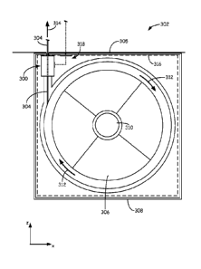
FIGS. 7-12 illustrate sensor assembly 200 in use with spooled container 202,
where sensor assembly 200 is an example of a suitable optical sensor assembly
for use in
system 10 (e.g., as sensor assembly 24 and/or sensor assembly 26, shown in
FIG. 1). As
shown in FIG. 2, spooled container 202 is a supply source containing filament
204, where
filament 204 is a marked filament. Examples of suitable marked filaments for
filament 204
include those discussed above (e.g., filaments 44 and 58).
Examples of suitable sources for spooled container 202 include those
discussed above for supply sources 20 and 22 (shown in FIG. 1), such as those
disclosed in
Swanson et al., U.S. Patent No. 6,923,634; Comb et al., U.S. Patent No.
7,122,246; Taatjes
et al, U.S. Patent Application Publication Nos. 2010/0096485 and 2010/0096489;
and
Swanson, U.S. Patent No. 8,403,658 and International PCT Publication No.
W02009/088995. In the shown embodiment, filament 204 may be wound around spool
206, which correspondingly may be retained in container housing 208. This
arrangement
allows filament 204 to be unwound from spool 206 while spool 206 rotates
around hub 210
within container housing 208, as represented by arrows 212. Filament 204 may
then pass
CA 02780317 2012-05-07
WO 2011/063216
PCT/US2010/057398
through sensor assembly 200 and exit spooled container 202 to a pathway of
system 10
(e.g., pathways 36 and 40), as represented by arrow 214.
Sensor assembly 200 includes subassemblies 216 and 218, which, in the
shown embodiment, are separate components that may engage with each other
during a
build operation. Subassembly 216 is retained within system 10, outside of
spooled
container 202, and contains the sensor electronics (not shown in FIG. 7) for
reading the
encoded markings of filament 204. Subassembly 218 is retained at least
partially within
container housing 208 of spooled container 202, and is the portion that
filament 204 passes
through prior to exiting spooled container 202. In the shown embodiment,
subassembly 218
is fully retained within container housing 208. As discussed below, when
spooled container
202 is loaded into a bay of system 10 (e.g., bays 20a and 22a), subassembly
216 may
engage with subassembly 218 to read encoded markings of filament 204 as
successive
portions of filament 204 pass through subassembly 218.
As shown in FIG. 8, subassembly 216 includes base block 220, circuit board
222, and waveguides 224. Base block 220 is a structural mount for retaining
circuit board
222. In alterative embodiments, base block 220 may be omitted and circuit
board 222 may
be directly mounted within system 10. Circuit board 222 is a control circuit
for
subassembly 216 and is configured to optically read the encoded markings of
filament 204
as filament 204 passes through subassembly 218 within spooled container 202.
Circuit
board 222 also desirably communicates with controller 32 over a communication
line (e.g.,
communication line 226), as discussed above for communication lines 38 and 42
(shown in
FIG. 1).
Waveguides 224 are a pair of waveguides (a single waveguide 224 is shown
in FIG. 8), which may be fabricated as an integral unit from a transparent or
translucent
plastic or glass material. Waveguides 224 are configured to route light from
one or more
light sources (not shown in FIG. 8) mounted on circuit board 222 to
subassembly 218, as
discussed below. Waveguides 224 are also configured to extend into an opening
within
container housing 208 (referred to as opening 228) to engage subassembly 218.
As further shown in FIG. 8, subassembly 216 is biased in the direction of
arrow 230 toward subassembly 218 by biasing members 232. Biasing members 232
are one
or more devices configured to bias subassembly 216 toward subassembly 218 when
spooled
container 202 is loaded to system 10. In the shown embodiment, biasing members
232 are
loaded springs located between base block 220 and the sidewall of the bay in
which supply
26
CA 02780317 2012-05-07
WO 2011/063216
PCT/US2010/057398
source 202 is loaded (referred to as sidewall 234). In alternative
embodiments, subassembly
216 may be mounted and biased from any suitable location within system 10.
System 10 may also include one or more latching mechanisms (not shown)
for retaining subassembly 216 in a retracted state against sidewall 234. In
these
embodiments, subassembly 216 may remain in the retracted state while spooled
container
202 is being loaded or unloaded from the bay of system 10. When spooled
container 202 is
loaded to the bay, the latching mechanism may be released, thereby allowing
subassembly
216 to engage subassembly 218.
Subassembly 218 includes window 236, waveguides 238, and filament guide
240, which may be fabricated as an integral unit from a transparent or
translucent plastic or
glass material. Window 236 may be secured to container housing 208 at opening
228,
which allows waveguides 224 of subassembly 216 to rest against window 236 at
opening
228 due to the bias in the direction of arrow 230. Waveguides 238 are a pair
of waveguides
(a single waveguide 238 is shown in FIG. 8) configured to route light from
waveguide 224
to filament guide 240. As discussed below, filament guide 240 includes a
channel for
filament 204 to pass through while being fed from spooled container 202 to
system 10. The
biasing of waveguides 224 against window 236 also allows the focal length of
sensor
assembly 200 to be repeatably fixed. This arrangement allows the light routed
through
waveguides 224 to also be routed through waveguides 238 to filament guide 240,
thereby
providing a darkfield illumination for filament 204.
As discussed below, the trench edges of the encoded markings of filament
204 scatter the light of the darkfield illumination in patterns based on the
encoded markings.
The scattered light may be optically detected at subassembly 216, thereby
allowing the
information retained in the encoded markings to be read based on the patterns
of the
scattered light. Subassembly 216 may then transmit signals relating to the
information to
controller 32 over communication line 226.
In one embodiment, subassembly 218 may form a moisture barrier with
container housing 208, allowing the interior of container housing 208 to
retain a low
moisture content. As shown, filament guide 240 includes inlet end 242 and
outlet end 244.
Inlet end 242 desirably forms a first moisture barrier with the interior walls
of container
housing 208, which define an interior region in which spool 206 may be
retained (referred
to as interior walls 246).
27
CA 02780317 2015-01-12
In some embodiments, spooled container 202 may include one or more liners
in addition to, or as an alternative to interior walls 246. Examples of
suitable liners include
those disclosed in Swanson, U.S. Patent No. 8,403,658 and International PCT
Publication
No. W02009/088995. In these embodiments, the liner may partially or fully
encase spool
206 and may be secured around inlet end 242 of filament guide 240 to maintain
a moisture
barrier within container housing 208.
Correspondingly, outlet end 244 desirably forms a second moisture barrier
with the exterior walls of container housing 208 (referred to as exterior
walls 248) at the
exit orifice of container housing 208 (referred to as exit orifice 250). The
pathway of
system 10 to extrusion head 18 (e.g., pathways 36 and 40, not shown in FIG. 8)
may also
form a moisture barrier at exit orifice 250 to maintain the low moisture
environment
between spooled container 202 and extrusion head 18.
The moisture barriers formed between container housing 208 and filament
guide 240 of subassembly 218 allow the interior region of spooled container
202 to be
maintained at a low humidity level to reduce the absorption of water into
filament 204.
Spooled container 202 may also include desiccant packs (not shown) within the
interior
region to maintain a dry environment. These implementations may allow filament
204 to
maintain a low moisture content (e.g., less than about 700 parts-per-million
by weight)
during storage and use.
FIG. 9 is a bottom perspective view of sensor assembly 200, where spooled
container 202 and base block 220 are omitted for ease of discussion. As shown,
waveguides
224 are a first pair of waveguides that are integrally connected at bridge
252. As further
shown, subassembly 216 also includes optical sensor 254, which may be secured
to circuit
board 222, as shown. Optical sensor 254 is a sensor configured to detect light
scattered
from the encoded markings of filament 204. Examples of suitable units for
optical sensor
254 include one or more imaging devices, such as a complementary metal-oxide-
semiconductor (CMOS) camera.
Optical sensor 254 desirably exhibits imaging capabilities to detect the
scattered light patterns from the encoded markings of filament 204. Suitable
imaging
capabilities may vary depending on the light intensity of the darkfield
illumination, the
encoding scheme used, and the dimensions of the encoded markings. For example,
an
marking pattern of multiple marks having a length of about 2.5 millimeters may
be imaged
with a 2:1 magnification onto a 640x480 pixel array. Examples of suitable
commercially
28
CA 02780317 2012-05-07
WO 2011/063216
PCT/US2010/057398
available CMOS cameras and corresponding image processors for circuit board
222 and
optical sensor 254 include those from Aptina Imaging Corporation, Grand
Cayman, KY;
and those from Toshiba Corporation, Minato, Tokyo, Japan.
As discussed below, subassembly 216 also includes a plurality of light
sources (not shown in FIG. 9) mounted on circuit board 222 at indentations in
waveguides
224 adjacent to circuit board 222 (referred to as indentations 256). In
alternative
embodiments, the light sources may be mounted at any suitable location within
system 10.
Waveguides 238 are a second pair of waveguides that are integrally
connected at bridge 258, where bridge 258 includes opening 260. Opening 260
provides an
access location for the light reflected from filament 204 (including the light
scattered from
the encoded markings of filament 204) to transmit through to reach optical
sensor 254. As
discussed below, one or more lenses may also be located between optical sensor
254 and
opening 260 for increasing or otherwise modifying the focus and magnification
of the
transmitted light.
As shown, when subassembly 216 engages subassembly 218, waveguides
224 substantially align with waveguides 238 along the x-axis. This allows the
light routed
through waveguides 224 to pass through window 236 to waveguides 238.
Waveguides 238
also route the received light, and the opposing end of waveguides 238 converge
toward each
other around filament guide 240. This causes the routed light to reflect at
least once prior
reaching filament 204 to provide a darkfield illumination, as discussed below.
FIG. 10 is an exploded perspective view of subassembly 216. As shown,
bridge 252 of waveguides 224 includes opening 262, which desirably aligns with
opening
260 (shown in FIG. 9) when subassembly 216 engages subassembly 218. As
discussed
above, one or both of openings 260 and 262 may retain one or more lenses for
increasing or
otherwise modifying the focus and magnification of the transmitted light.
As further shown in FIG. 10, light sources 264 are mounted to circuit board
222 and desirably align with indentations 256 of waveguides 224. Light sources
264 may
be any suitable type of light source to provide a darkfield illumination for
filament 204,
such as light emitting diodes (LEDs). Additionally, while shown as two pairs
of LEDs,
subassembly 216 may include a variety of different numbers of light sources
for providing a
darkfield illumination for filament 204. In one embodiment, light sources 264
may include
multiple color LEDs, such as red, green, and blue LEDs, which may be
selectively used to
illuminate filament 204.
29
CA 02780317 2012-05-07
WO 2011/063216
PCT/US2010/057398
FIG. 11 is a perspective view of subassembly 218. As shown, window 236
of subassembly 218 also includes opening 266, which is aligned with opening
260 (shown
in FIG. 9), and desirably aligns with opening 262 (shown in FIG. 10) when
subassembly
216 engages subassembly 218. Openings 266 may also retain one or more lenses
for
increasing or otherwise modifying the focus and magnification of the
transmitted light.
FIG. 12 is a bottom view of sensor assembly 200, where subassembly 216 is
engaged with subassembly 218. During operation, filament 204 may be fed
through the
channel of filament guide 240 (referred to as channel 268). Channel 268
desirably has
dimensions that allow filament 204 to pass through filament guide 240 without
undue
friction while also desirably confining filament 204 to the object plane of
optical sensor 254
such that the grazing angle input light scatters from the encoded markings of
filament 204.
In embodiments in which filament 204 is a marked cylindrical filament (e.g.,
filament 44), suitable average inner diameters for channel 268 range from
about 1.0
millimeter (about 0.04 inches) to about 3.8 millimeters (about 0.15 inches),
and with
particularly suitable average diameters ranging from about 1.3 millimeters
(about 0.05
inches) to about 2.5 millimeters (about 0.1 inches).
In embodiments in which filament 204 is a marked non-cylindrical filament
(e.g., filament 58), channel 268 may include a cross section that
substantially matches the
geometry of the marked non-cylindrical filament. For example, in embodiments
in which
the marked non-cylindrical filament has a rectangular cross section (e.g.,
filament 58),
channel 268 desirably has a rectangular cross section with a width-to-
thickness aspect ratio
that substantially matches the aspect ratio of the filament. In these
embodiments, suitable
average widths for channel 268 range from about 1.3 millimeters (about 0.05
inches) to
about 12.7 millimeters (about 0.50 inches), with particularly suitable average
widths
ranging from about 3.8 millimeters (about 0.15 inches) to about 10.2
millimeters (about
0.40 inches). Suitable average thicknesses for channel 268 range from about
0.25
millimeters (about 0.01 inches) to about 2.5 millimeters (about 0.1 inches),
with particularly
suitable average thicknesses ranging from about 0.51 millimeters (about 0.02
inches) to
about 1.8 millimeters (about 0.07 inches).
The encoding scheme used desirably allows the encoded markings to be read
by sensor assembly 200 without substantially affecting the drive rate of
filament 204 to
extrusion head 18. The drive rate of filament 204 to extrusion head 18 may
vary depending
the extrusion parameters in extrusion head 18 and the dimensions of filament
204.
CA 02780317 2015-01-12
Examples of suitable drive rates range from about 2.5 millimeters/second
(about 100
mils/second) to about 7.6 millimeters/second (about 300 mils/second).
As filament 204 passes through channel 268, light is emitted from light
sources 264, which are routed through waveguides 224 and 238 toward filament
guide 240.
The converging orientations of waveguides 238 desirably cause the routed light
to reflect at
least once prior reaching filament 204 to provide a darkfield,illumination. In
particular, the
light desirably reflects at least once before grazing the exterior surface of
filament 204
within filament guide 240. When particular rays of the light reach the trench
edges of the
encoded markings of filament 204, the trench edges cause these particular rays
to scatter.
Accordingly, the scattering of the light follows the pattern of the encoded
markings.
A portion of the reflected and scattered light may then transmit through
openings 266, 260, and 262 (and through any lenses retained therein) toward
optical sensor
254. Optical sensor 254 may image the received light, which, which may then be
processed
by circuit board 222 and/or controller 32 (via communication line 226) to
decode the
information from the image patterns based on the encoding scheme used.
Controller 32
may then use the received information to assist in the operation to build 3D
model 28
and/or support structure 30, as discussed above.
In another embodiment, the sensor assemblies may be retained fully within
supply sources 20 and 22, respectively. For example, FIG. 13 illustrates
sensor assembly
300 in use with spooled container 302, where sensor assembly 300 is an example
of a
suitable sensor assembly for use in system 10 (e.g., as sensor assembly 24
and/or sensor
assembly 26, shown in FIG. 1). As shown, spooled container 302 is a supply
source
containing filament 304, where filament 304 is a marked filament. Examples of
suitable
marked filaments for filament 304 include those discussed above (e.g.,
filaments 44 and
58). In the shown example, spooled container is mounted in a bay of system 10
(e.g., bay
20a), which includes front wall 305.
Examples of suitable sources for spooled container 302 include those
discussed above for supply sources 20 and 22 (shown in FIG. 1), such as those
disclosed in
Swanson et al., U.S. Patent No. 6,923,634; Comb et al., U.S. Patent No.
7,122,246; Taatjes
et al, U.S. Patent Application Publication Nos. 2010/0096485 and 2010/0096489;
and
Swanson, U.S. Patent No. 8,403,658 and International PCT Publication No.
W02009/088995. In the shown embodiment, filament 304 may be wound around spool
306, which correspondingly may be retained in container housing 308. This
arrangement
31
CA 02780317 2015-01-12
allows filament 304 to be unwound from spool 306 while spool 306 rotates
around hub 310
within container housing 308, as represented by arrows 312. Filament 304 may
then pass
through sensor assembly 300 and exit spooled container 302 to a pathway of
system 10
(e.g., pathways 36 and 40), as represented by arrow 314.
In the shown embodiment, spooled container 302 also includes liner 316,
which includes one or more films configured to provide a moisture barrier
within container
housing 308. Examples of suitable liners for liner 316 include those disclosed
in Swanson,
U.S. Patent No. 8,403,658 and International Publication No. W02009/088995.
As shown, sensor assembly 300 is fully retained within housing 308, and
within liner 316. While sensor assembly 300 is illustrated in FIG. 13 as being
located in a
particular location within housing 308 and liner 316 (i.e., in an upper-left
corner in the view
shown in FIG. 13), sensor assembly 300 may alternatively be disposed in other
locations
within housing 308 and liner 316 such that filament 304 may pass through (or
adjacent to)
sensor assembly 300 prior to exiting liner 316 and/or housing 308.
Sensor assembly 300 may receive electrical power from and/or communicate
with system 10 via signal lines 318 or other suitable power and/or signal
communication
techniques. For example, signal lines 318 may be arranged in an engagement
manner as
disclosed in one or more of Swanson et al., U.S. Patent No. 6,923,634; Comb et
al., U.S.
Patent No. 7,122,246; Taatjes et al, U.S. Patent Application Publication Nos.
2010/0096485
and 2010/0096489; and Swanson, U.S. Patent No. 8,403,658 and International PCT
Publication No. W02009/088995. In the shown embodiment, a portion of signal
lines 318
desirably extends through liner 316 in a scalable manner that maintains the
moisture
barrier.
During use, filament 304 passes through sensor assembly 300 prior to exiting
liner 316 and housing 308. As such, sensor assembly 300 may read the encoded
markings
of filament 304 and transmit signals relating to the read markings to system
10. Sensor
assembly 300 may read the encoded markings of filament 304 using a variety of
different
techniques, which may vary depending on the particular marking techniques used
to form
the encoded markings along filament 304.
FIG. 14 is a schematic illustration of a suitable embodiment of sensor
assembly 300, which is configured to read the encoded markings based on far-
field
diffraction patterns. As shown, in this embodiment, filament 304 includes
encoded
markings 320 formed on surface 322, where the pattern of encoded markings 320
function
32
CA 02780317 2012-05-07
WO 2011/063216
PCT/US2010/057398
as diffraction gratings having different indices of refractions from the
remaining portions of
surface 322. Encoded markings 320 may be formed on or in surface 322 using one
or more
of the techniques discussed above. In one embodiment, the degree of cross
linking of the
precursor material may be locally modified by ultraviolet light to varying the
index of
refraction at the locations of encoded markings 320.
As further shown, sensor assembly 300 includes light emitter 324 and optical
detectors 326. In alternative embodiments, sensor assembly 300 may include
multiple light
emitters and/or a different number of optical detectors 326. In the shown
embodiment,
optical detectors 326 are desirably positioned such that diffracted beams of
light from
encoded markings 320 are directed to optical detectors 326. The directions of
the diffracted
beams of light from encoded markings 320 may correspondingly be predetermined
by the
encoding pattern(s) of encoded markings 320.
During operation, while successive segments of filament 304 pass through
sensor assembly 300 in the direction of arrow 314, light emitter 324 generates
light beam
328 toward filament 304. Encoded markings 320 are configured to diffract all
or a portion
of the incident light beam 328 into separate diffracted beams 330. Diffracted
beams 330
may be separately detected by optical detectors 326, thereby generating
electrical signals
indicative of the information encoded in encoded markings 320. The information
may then
be transmitted to controller 32 of system 10 (shown in FIG. 1) over electrical
connection
lines 318 (shown in FIG. 13) and communication line 36 or 40 (shown in FIG.
1).
Controller 32 may then use the received information to assist in the operation
to build 3D
model 28 and/or support structure 30, as discussed above.
As discussed above, the marked consumable materials of the present
disclosure allow information to be recorded in the consumable materials
themselves. The
encoded markings may contain a variety of information relating to the marked
consumable
materials and/or to the operations of the direct digital or additive
manufacturing systems
(e.g., system 10). Additionally, the sensor assemblies (e.g., sensor
assemblies 24, 26, 200,
and 300) are configured to read the encoded markings from successive portions
of the
marked consumable materials as the marked consumable materials are fed to the
additive
manufacturing systems. This allows the additive manufacturing systems to use
the
information in the encoded markings for a variety of different purposes, such
as for building
3D models and/or support structures.
33
CA 02780317 2015-08-10
Although the present disclosure has been described with reference to
preferred embodiments, workers skilled in the art will recognize that changes
may he made
in form and detail without departing from the scope of the disclosure, which
is defined in
the appended claims.
34