Note: Descriptions are shown in the official language in which they were submitted.
CA 02780323 2012-05-10
PCT/AU20.10/001329
Received 05/08/2011
A1:01780
RADIO FREQUENCY IDENTIFICATION READER ANTENNA HAVING A
DYNAMICALLY ADJUSTABLE Q-FACTOR
FIELD OF THE INVENTION
(00011 The present invention relates to radio frequency identification
(RFID) systems, and
more particularly to RFID readers with resonant antennas.
BACKGROUND
(0002] Passive low frequency RFID readers and tags use operating principles
that are well-
know to those of ordinary skill in the art, and that are described in
extensive detail in several
seminal inventions, including U.S. Patent 1,744,036 to Braid, U.S. Patent
3,299,424 to Vinding,
U.S. Patent 3,713,146 to Cardullo, and U.S. Patent 5,053,774 to Schuermann,
and in textbooks
such as Fmkenzeller, "RFID Handbook" (1999).
[00031 International Standards Organization (ISO) Standard 11785, "Radio
frequency
identification of animals ¨ Technical Concept" (1996) defmes the technical
principles for
communications between reader devices and two types of electronic passive
identification
transponders. Both transponder types contain identification information stored
in binary form,
which is conveyed to the reader when a transponder is suitably activated by
the reader. ISO
11785 relates to radio frequency identification (RFID) systems, comprising low
frequency reader
devices and passive, inductively powered identification tags (i.e., "ID
tags"). In RED systems
of this type, the reader device generates a tag activation signal, and
receives identification data
signals from the ID tag. Such a reader device can use separate transmit and
receive antenna
elements to perform these functions. Additional technical details are provided
in ISO Standard
.11785.
(00041 Readers in which a single antenna performs both transmit and receive
functions are
very cost effective and efficient, and comprise the most common design
implementation in low-
frequency RFID readers. However, when a single antenna is used for both
transmit and receive
purposes, the antenna's design characteristics must be inevitably compromised,
and the antenna
performs less efficiently than when it can be designed optimally for a single
purpose.
-1-
=
AMENDED SHEET
IPEA/AU
CA 02780323 2012-05-10
PCT/AU2010/001329
Received 05/08/2011
A1:01780
[0005] A conventional RFID reader including a single resonant antenna is
shown in FIG. 1.
The RFID reader [100] includes electronic circuitry, which generates an
activation signal
(usually a single frequency unmodulated signal) using a signal source [101]
and an amplifier
[102] to drive a resonant antenna circuit [103]. This activation signal is
manifested as a time-
varying electromagnetic field, which couples with = the ID tag [105] by means
of the
electromagnetic .field's magnetic . field component [104a). The ID tag [105].
converts this
magnetic field into an electrical voltage and current, and uses this
electrical power to activate its
internal electronic circuitry. Using any of several possible modulation
schemes, the ID tag
conveys binary encoded information stored within it back to the reader via
magnetic field [104b),
where the detector and utilization circuit [106] converts this binary code
into alphanumeric
format tag data (107) in accordance with some prescribed application.
[0006] Fig. 2 shows the composition of Fig. l's resonant antenna circuit
[103] in schematic
detail within the dashed line [212]. The resonant antenna circuit includes at
least one capacitor C
[213] connected to at least one inductor L [214], where the values of C and L
are selected such
that the circuit resonates at the signal source frequency [210] as amplified
by amplifier [211].
Inductor L is also constructed in such a manner that it creates a magnetic
field [215] within its
immediate vicinity.
[0007[ ISO Standard 11785 defines two types of transponder occlmologies,
which arc
designated "full-duplex" (TDX-B") and "half-duplex" ("HDX"). In the described
manners that
follow, for FDX-B and HDX transponders, respectively, activation energy is
transferred to the
transponder from the reader, and identification code information is
transferred to the reader from
the transponder through the mutual coupling of a magnetic field.
[0008] The FDX-B transponder communicates to the reader by amplitude
modulating the
activation signal it receives with a binary pattern representative of the data
stored within the tag.
Amplitude modulation imposes variations on the activation signal's magnitude,
and the reader is
equipped with sensing circuity capable of detecting these magnitude
variations. The term "full-
duplex" is indicative of the fact that the FDX-B transponder sends its
identification code
information during the time when it is receiving the activation signal from
the reader.
[0009) An HDX transponder typically contains its own micro-power radio
frequency
transmitter, which is powered with energy received from the reader's
activation signal and stored
-2-
AMENDED SHEET
IPEA/AU
CA 02780323 2012-05-10
PCT/AU2010/001329
Received 05/08/2011
A1:01780
=
internally in a capacitor component. Once the activation signal ceases, the
HDX transponder
emits a very low strength radio signal, comprising a frequency shift keyed
("FSK") modulation
scheme. Specifically, the binary identification code information contained in
the HDX tag is
serially output such that the occurrence of a binary "1" results in the HDX
tag's radio signal
being 124.2 KHz and a binary "0" results In the tag's radio signal being 134.2
KHz. The reader
detects this FSK signal and derives from it the HDX transponder's
identification code. The term
"half-duplex" is indicative that the reader and the HDX transponder exchange
the activation
signal and the identification code signal in alternating time intervals.
100101 An ISO compliant reader has the capability to activate and detect
both FDX-B and
HDX typc transponders when present. To accomplish this, the ISO compliant
reader transmits
an activation signal, consisting of a 134.2 kilohertz (KHz) sinusoid, which is
switched ON and
OFF in a prescribed pattern in accordance with ISO 11785. During the interval
in which the
134.2 KHz signal is ON, the FDX-B transponder is activated and it transmits
its identification
code signal cyclically for as long as the activation signal is present. During
this ON interval
also, an HDX transponder charges its internal capacitor. Subsequently, during
the interval in
which the 134.2 KHz activation signal is OFF, the FDX-B transponder remains
dormant, and the
HDX transponder transmits its identification code sequence.
100111 Figs. 3(a) through 3(c) illustrate the frequency spectrum
characteristics of an RFID
system conforming with ISO 11785. Fig. 3(a) shows the spectra for the HDX tag,
where the
activation signal [310] appears at 134.2 KHz, and where the HDX transponder
frequencies
appear at 124.2 KHz [311] and 134.2 KHz [312]. Since the activation signal and
the HDX
transponder signals are time interleaved, the 134.2 KHz activation signal
[310] and the 134.2
KHz transponder signal [312] typically do not occur simultaneously. Thus, the
reader's receive
circuitry is able to detect the transponder frequency without interference
from its own activation
signal.
[0012] Fig. 3(b) shows the spectra for the FDX-B tag, where the activation
signal [320]
appears at 134.2 KHz, and where the FDX-B transponder's amplitude modulation
appears as
sidebands [323] close to the 134.2 KHz carrier. As is well known to those of
ordinary skill in the
art, amplitude modulation sidebands appear symmetrically around the modulated
carrier signal,
and for FDX-B specifically, these sidebands appear at * 2.097 KHz and 4.194
KHz. Because
-3-
AMENDED SHEET
1PEA/AU
CA 02780323 2012-05-10
PCT/AU2010/001329
Received 05/08/2011
A1:01780
the activation signal [320] and the data signal [323] are distinct
frequencies, they can occur
simultaneously, and the reader is able to separate the two signals, thus
recovering the tag data
contained in these sideband frequencies.
[0013) In Fig 3(c), the frequency spectral characteristics from Fig 3(a)
and Fig 3(b) are
shown together, along with curve [335], which characterizes the frequency
response of the
reader's resonant antenna circuit [212] of Fig. 2. For the resonant antenna
circuit to perform well
as both transmitter and receiver, and for both HDX and FDX-B tags, the antenna
design is
typically a compromise. The resulting resonant antenna [212], [335] functions
adequately as
both transmitter and receiver for HDX and for FDX-B, but in having a fixed Q-
factor and a fixed
resonant frequency that works for all its functions, it is not optimized for
each individual
function. For example, in order to be an efficient 134.2 KHz activation signal
transmitter, the
resonant antenna circuit is ideally characterized by a very high quality
factor, or "high-Q", as it is
known to those skilled in the art. The "Q-factor" of an inductor used in a
resonant circuit (such
as the antenna is) describes "sharpness" or "selectivity" of the inductor.
Mathematically, the
resonant antenna's Q is calculated according to the formula:
Q¨; sfL =L/C)"
where f is the resonant frequency, L is the inductor's inductance value, C is
the resonant
capacitance, and R is the inductor's resistance. Furthermore, the bandwidth of
a resonant
antenna circuit using such an inductor is:
BW= j/Q
100141 Thus, a resonant antenna circuit has a very high-Q when its
resistance is very low, but
this very high-Q implies a very narrow bandwidth. As shown in Fig 3(c), a
resonant antenna
circuit with a very high-Q exhibits a narrow bandwidth as depicted by the
curve [336]. A very
high-Q resonant antenna circuit is very effective and efficient for
transmitting a single frequency
activation signal [330], but has insufficient bandwidth to capture the HDX
[331], [332] and the
FDX-B [333) transponder spectra. Thus, a very high-Q antenna typically does
not work
satisfactorily as both a transmitter and a receiver antenna.
-4-
AMENDED SHEET
IPEAJAU
CA 02780323 2012-05-10
PC T/AU2010/001329
Received 05/08/2011
A1:01780
[0015] If the resonant antenna circuit's Q is decreased such that it
exhibits the bandwidth
depicted by curve [334], the antenna is less efficient in transmitting the
activation signal, but
provides sufficient bandwidth to capture the FDX-B transponder spectra [333].
However, the
lower HDX data frequency at 124.2 KHz [331] lies outside the antenna's
response curve, and
typically will not be effectively captured.
[00161 If the resonant antenna's Q-factor is decreased even further such
that it exhibits the
bandwidth depicted by curve [335] in Fig 3(c), this "low-Q" wide-bandwidth
characteristic will
adequately capture both the HDX [331], [332] and FDX-B [333] transponder
spectra, but the
antenna does not transmit the activation signal efficiently. Furthermore, this
wider bandwidth
makes the antenna more susceptible to interference signals from other nearby
electromagnetic
radiating sources, and this can be especially detrimental to FDX-B
performance.
[0017] From the curves [334], [335], and [336] in Fig 3(c), it is apparent
that as the resonant
antenna's Q-factor is increased to improve transmit efficiency and
interference rejection, the
antenna becomes less suitable for transponder signal reception. However, if
the resonant
antenna's Q-factor is dynamically altered, the antenna can function more
efficiently as
transmitter and receiver for both HDX and FDX-B type transponders.
100181 An improvement to the resonant antenna circuit thus far described is
disclosed in U.S.
Patent 7,528,725 to Stewart, the fundamental principles of which are
reproduced herein in Figs.
4(a) through 4(d). The '725 Stewart patent proposes the use of a resonant
antenna having an
intermediate Q-factor, such as that depicted in Fig. 3(c) by curve [334] and
in Fig. 4(b) by curves
[414] and [415]. During the transponder activation period when FDX-B
transponder data is
present, the antenna's resonant frequency is set to 134.2 KHz [410], and it's
Q-factor provides
sufficient bandwidth to capture the FDX-B transponder spectra [413]. When the
activation
signal ceases, and the HDX transponder signal becomes present, the antenna's
resonant
frequency is lowered to nominally 129.2 KHz as shown by curve [415], thus
allowing the HDX
transponder spectra [411], [412] to be captured.
100191 Fig. 4(a) illustrates an electrical circuit that can accomplish the
resonant frequency
shifting described in the '725 Stewart patent using the activation signal's
on/off state. When the
activation signal [406] is present, it drives the resonant circuit comprising
capacitor C [404] and
inductor L [405]. The activation signal bypasses inductor 1.4 [403] through
diodes Di [401] and
-5-
AMENDED SHEET
1PEA/AU
CA 02780323 2012-05-10 =
PCT/AU2010/001329
Received 05/08/2011
A1:01780
1)3 [402], and so the resonant frequency of the antenna is determined by the
values of C [404]
and L [405], which are selected to resonate at 134.2 KHz. When the activation
signal is absent,
diodes Di [401] and D2 [402] become high impedances, and thus inductor LT
becomes part of the
antenna circuit. The resonant frequency of the antenna is now determined by
the values of C
[404], L [405], and LT [403], which are selected to resonate at 129.2 KHz.
Thus, as the
activation signal (406) is switched on and off, the antenna's resonant
frequency dynamically
shifts between 134.2 KHz [414] and 129.2 KHz [415].
100201 The /25 Stewart patent also discloses the possible change in Q-
factor during the
resonant frequency shifting process, as shown in Figs. 4(c) and 4(d). If
inductor LT [425] has a
non-zero resistance value RT [426], or if a discrete resistive component is
inserted into the circuit
to create resistance RT [426], the resulting effect is depicted in Fig. 4(d).
During the activation
signal on interval, the antenna has a resonant frequency of 134.2 KHz and a Q-
factor as shown
by curve [434]. When the activation signal is turned off, inductance Li [425]
and resistance RT
(426] are inserted into the antenna's resonant circuit, thus altering the
antenna's characteristic to
that shown by curve [435] in Fig. 4(d),
SUMMARY OF THE INVENTION
100211 Systems and methods in accordance with embodiments of the invention
incorporate
resonant antennas that exploit the benefits of alteration of Q-factor during
the transponder
activation and interrogation interval. In several embodiments, improved
reading distance is
achieved by dynamically adjusting, during the tag activation and tag data
transmission interval's,
the antenna's Q-factor, thereby increasing the efficiency of the activation
signal, and improving
the antenna's effective bandwidth for tag data reception. In various
embodiments, the activation
signal is a fixed frequency activation signal and the reader is configured to
receive transponder
signals from ISO compliant HDX and FDX-B signals through the dynamic
adjustment of the
antenna's Q-factor at various points in the interrogation period.
100221 While the present invention is intended primarily for use in readers
that incorporate
both types of RFID technologies disclosed in ISO 11785, the invention is also
useful in readers
equipped with only either one of these technologies. Moreover, while the
present invention is
primarily and advantageously applicable to readers in which one antenna
performs both
-6-
AMENDED SHEET
1PEA/AU
CA 02780323 2012-05-10
PCT/AU2010/001329
Received 05/08/2011
A1:01780
transmitting and receiving functions, the invention is also applicable to
readers having multiple
tintennas, including readers in which at least one of the antennas performs
both transmitting and
receiving functions.
100231 One embodiment of the invention includes a signal source configured
to drive a
resonant antenna, and a dynamic switching circuit configured to set the Q-
factor of the resonant
antenna to a first value during the transmission of the activation signal. In
addition, the dynamic
switching circuit is configured to set the Q-factor of the resonant antenna to
a second value
below the first Q-factor value during the transmission of the activation
signal and detection of a
data signal from a full duplex transponder.
(0024) In a further embodiment, the reader transmits an activation signal
configured to
activate half duplex and full duplex transponders. In addition, the dynamic
switching circuit is
also configured to set the Q-factor of the resonant antenna to a third value
below the first Q-
factor value when the RFID reader is not transmitting the activation signal.
[00251 In another embodiment, the second Q-factor value is higher than the
third Q-factor
value.
[0026) In a still further embodiment, the dynamic switching circuit further
includes a
dynamic tuning network configured to time the resonant antenna to a first
resonant frequency
value during transmission of the activation signal and to a second resonant
frequency value when
the RFED reader is not transmitting the activation signal.
[00271 In still another embodiment, the resonant antenna is multi-filar and
the dynamic
switching circuit is configured to control the Q-factor of the multi-filar
resonant antenna by
controlling the filers that are incorporated into the resonant antenna
circuit.
100281 In a yet further embodiment, the resonant antenna is a tri-filar
antenna and the
dynamic switching circuit is configured to select the Q-factor of the resonant
antenna by
incorporating one or more filers into the resonant antenna circuit.
100291 In yet another embodiment, the resonant antenna is a bi-filar
antenna, where one of
the filars is connected in series with a resistor and the dynamic switching
circuit is configured to
select the Q-factor of the resonant antenna by incorporating one or more
filers into the resonant
antenna circuit.
-7-
AMENDED SHEET
lPEA/AU
CA 02780323 2012-05-10
PCVAU2010/001329
Received 05/08/2011
Al :01780
[0030] In a further embodiment again, the resonant antenna includes
multiple resonant
circuits and the dynamic switching circuit is configured to independently
drive each of the
resonant circuits.
(00311 In another embodiment again, the resonant antenna includes a
switched resistor and
the dynamic switching circuit is configured to set the Q-factor of the
resonant antenna using the
switched resistor.
[0032J A further additional embodiment includes setting the Q-factor of
the resonant antenna
at a first value during the transmission of an activation signal, decreasing
the Q-factor of the
resonant antenna during receipt of a data signal from any full duplex
transponders present during
the transmission of the activation signal, increasing the Q-factor of the
resonant antenna to the
first value during the remainder of the transmission of the activation signal,
and capturing data
from the received data signal.
100331 In another additional embodiment, the process further includes
interrogating half
duplex transponders by decreasing the Q-factor of the resonant antenna upon
stopping the
transmission of the activation signal, and remaining at a reduced level during
receipt of a data
signal from any half duplex transponders present.
100341 In a still yet further embodiment, the Q-factor of the resonant
antenna during data
capture from any full duplex transponders present is greater than the Q-factor
of the resonant
antenna during data capture from any half duplex transponders present.
100351 In still yet another embodiment, the resonant antenna is a multi-
filar antenna.
= 100361 In a still further embodiment again, setting the Q-
factor of the resonant antenna at a
first value during the transmission of an activation signal includes
incorporating at least two of
the filters of the mull-flat antenna into the resonant antenna circuit,
decreasing the Q-factor of
the resonant antenna during receipt of a data signal from any full duplex
transponders present
and during the transmission of the activation signal includes incorporating at
least one Of the
filers of the multi-filar antenna into the resonant antenna circuit, and
decreasing the Q-factor of
the resonant antenna upon stopping the transmission of the activation signal
includes
incorporating at least one of the friars of the multi-filar antenna into the
resonant antenna circuit.
[00371 In still another embodiment again, the resonant antenna is a bi-
filar antenna, where a
resistor is connected in series with one of the filers, setting the Q-factor
of the resonant antenna
-8-
AMENDED SHEET
IPEA/AU
CA 02780323 2012-05-10
PCT/AU2010/001329
Received 05/08/2011
=
A1:01780
at a first value during the transmission of an activation signal includes
incorporating the two
filers into the resonant antenna circuit so that the resistor is not
incorporated within the resonant
antenna circuit, decreasing the Q-factor of the resonant antenna during
receipt of a data signal
from any full duplex transponders present and during the transmission of the
activation signal
comprises incorporating a primary filar into the resonant antenna circuit so
that the resistor is not
incorporated in the resonant antenna circuit, and decreasing the Q-factor of
the resonant antenna
upon stopping the transmission of the activation signal comprises
incorporating the primary filar
and the resistor into the resonant antenna circuit.
[0038] In a still further additional embodiment, the resonant antenna
includes multiple
resonant circuits.
10039] In still another additional embodiment, setting the Q-factor of the
resonant antenna to
a first level comprises driving at least two of the resonant circuits during
the transmission of an
activation signal.
[0040J In a yet further embodiment again, the resonant antenna includes a
switched resistor.
[0041J In yet another embodiment again, decreasing the Q-factor of the
resonant antenna
upon stopping the transmission of the activation signal comprises switching
the resistor into the
resonant antenna circuit.
[0042J A yet further additional embodiment also includes tuning the
resonant antenna to a
first resonant frequency value during transmission of the activation signal,
and tuning the
resonant antenna to a second resonant frequency value when the RFID reader is
not transmitting
the activation signal.
[00431 Yet another additional embodiment includes a signal source
configured to drive a
resonant antenna, and a dynamic switching circuit configured to set the Q-
factor of the resonant
antenna to a first value during the transmission of the activation signal. In
addition, the dynamic
switching circuit is configured to set the Q-factor of the resonant antenna to
a second value
below the first value in response to detection of a data signal from a full
duplex transponder, the
dynamic switching circuit is also configured to set the Q-factor of the
resonant antenna to a third
value below the second value when the RFID reader is not transmitting the
activation signal, and
the resonant antenna is multi-filar and the dynamic switching circuit is
configured to control the
=
=
-9-
AMENDED SHEET
1PEA/AU
CA 02780323 2012-05-10
PCT/AU2010/001329
Received 05/08/2011
Al :01780
Q-factor of the multi-filar resonant antenna by controlling the filers that
are incorporated into the
resonant antenna circuit.
BRIEF DESCRIPTION OF THE FIGURES
[0044] Fig. 1 illustrates the basic components of a conventional passive
RF1D system.
10045] Fig. 2 illustrates a resonant antenna circuit for a single antenna
coil reader
[0046] Figs. 3(a) through 3(c) illustrate the frequency spectra of a
reader's activation signal
and transponder signal frequencies for HDX and FDX-B transponders. Fig. 3(c)
illustrates the
signal spectra of Figs. 3(a) and 3(b) with respect to the characteristic
frequency responses of
three different reader resonant antennas.
[0047] Figs. 4(a) through 4(d) illustrate prior art methods that alter the
resonant frequency
and the Q-factor of the resonant antenna circuit in synchronization with the
activation signal's
on/off state.
[00481 Fig. 5(a) illustrates three Q-factor response curves for resonant
antenna circuits in
accordance with embodiments of the invention.
10049] Fig. 5(b) illustrates a method of Q-factor variation over the course
of the reader's
interrogation cycle in accordance with an embodiment of the invention.
[0050] Figs. 6(a) and 6(b) illustrate electrical schematic diagrams for two
RFD) reader
circuits configured to vary resonant antenna Q-factor in accordance with
embodiments of the
invention.
[00511 Figs. 7(a) and 7(b) illustrate how the Q-factor variation technique
of the present
invention as shown in Figs. 6(a) and 6(b) can be combined with dynamic tuning
in accordance
with embodiments of the invention.
10052] Fig. 7(c) illustrates how the resonant antenna's response curve
behaves with dynamic
tuning as compared to .Fig. 5(a).
DETAILED DESCRIPTION OF THE INVENTION
[0053] Turning now to the drawings, systems and methods for reading RFID
transponders
utilizing readers in which the Q-factor of the resonant antenna of the reader
shifts over the course
-10-
AMENDED SHEET
[PEA/AU
CA 02780323 2012-05-10
PCT/AU2010/001329
Received 05/08/2011
A 1 :01780
of the reader's interrogation cycle in response to the detection of data from
FDX and HDX RFID
transponders in accordance with embodiments of the invention are illustrated.
In several
embodiments, a high Q-factor is used during the transmission of an activation
signal and is
shifted to a lower Q-factor in response to the detection of data from an FDX
tag. In many
embodiments, the Q-factor is further reduced during periods in which the
activation signal is
absent and in which data is detected from an HDX tag. In a number of
embodiments, the RFID
reader adjusts the Q-factor of its resonant antenna by switching conductors in
a multi-filar
antenna. In several embodiments, the RFID reader also adjusts the tuning of
the resonant
antenna during the interrogation cycle. In further embodiments, variations in
Q-factor are
achieved using a plurality of resonant circuits. In many embodiments, a series
resistance is
switched in and out of a resonant antenna circuit to vary Q-factor. RFID
readers and processes
for shifting the Q-factor of a resonant antenna of an RFID reader in
accordance with
embodiments of the invention are discussed further below.
Processes for readin2 RFID transponders
[0054] Fig. 5(a) reproduces the resonant antenna response curves
illustrated in Fig. 3(c), as
they relate to the present invention. In Fig. 5(a), curve QA [506] represents
a high Q-factor
associated with an antenna whose bandwidth is sufficient for transmitting the
activation signal
frequency [500], but that has insufficient bandwidth for optimal reception of
either FDX-B data
signal frequencies [503] or HDX data signal frequencies [501], [502).
[0055] Curve QF [504] in Fig. 5(a) exhibits an intermediate Q-factor, being
less efficient for
transmitting the activation signal [500], but having sufficient bandwidth for
capturing the FDX-B
data frequencies [503] and having insufficient bandwidth for capturing of the
lower HDX signal
frequency [501]. Curve QH [505] exhibits a low Q-factor, which is even less
efficient than curve
QF [504] for transmitting the activation signal [500], but which now has
sufficient bandwidth to
capture both HDX data frequencies [501], (502).
[0056] While curve QH [505] also adequately captures FDX-B data frequencies
[503], curve
Qv [504] is preferable inasmuch as curve Qp [504] exhibits higher gain and
less bandwidth, both
of which improve the signal-to-noise ratio of the FDX-B data frequencies
[503].
-11-
AMENDED SHEET
IPEA/AU
CA 02780323 2012-05-10
PCT/AU2010/001329
Received 05/08/2011
AI:01780
[00571 Processes for reading RFID transponders in accordance with several
embodiments of
= the invention involve shifting the Q-factor of the resonant antenna(s) of
the reader between Q-
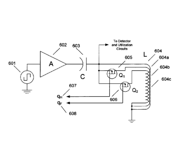
factors of QA. Qr. and QH respectively. Although much of the following
discussion is written
from the perspective of changing the Q-factor of a single resonant antenna,
RFID readers in
accordance with embodiments of the invention can utilize more than one
resonant antenna and
many RFID readers in accordance with embodiments of the invention utilize
three resonant
antennas having Q-factors of QM Qp, and QH. By utilizing different Q-factors
during different
phases of an interrogation cycle, RFID readers in accordance with embodiments
of the invention
can achieve significantly increased read ranges. In the context of ISO 11785,
the shifting
scheme over the course of the interrogation cycle involves the following
sequence:
(a) Set to level QA [506] at the commencement of activation signal ON
(b) Decrease to level Qp [504] during activation signal ON and FDX-B data
capture
(c) Set back to level QA [506] for the remainder of activation signal ON
(d) Set to level QH 1505] at the commencement of activation signal OFF
(e) Remain at level QH [505] during HDX data capture and activation signal OFF
[00581 In the aforesaid manner, the resonant antenna's Q-factor to be
adjusted to improve its
performance for transmit and receive purposes. Examples of the utilization of
different resonant
antenna Q-factors during various interrogation cycles and different
implementations of RFID
readers in accordance with embodiments of the invention are discussed below.
An exemplary interrogation cycle
(0059) Variation of resonant antenna Q-factor [510] over the course of
several interrogation
cycles and as a function of transponder data detection in accordance with an
embodiment of the
invention is illustrated in Fig. 5(b). The interrogation cycle illustrated in
FIG. 5(b) is in
accordance with ISO 11785. The vertical axis of Fig. 5(b) represents the Q-
factor on which three
relative levels QA [511], QF [512], and QH [513) are indicated. The horizontal
axis represents the
state of the activation signal as being either on or off.
[0060) Al the commencement of activation signal on interval [514], the
resonant antenna Q-
factor is initially set to its highest level QA [511] for a brief interval
[515], which typically occurs
-12-
AMENDED SHEET
IPEAJAU
CA 02780323 2012-05-10
PCT/AU2010/001329
Received 05/08/2011
A1:01780
for only a few milliseconds. The associated highest activation signal level
provides the
maximum magnetic field strength for activating a transponder within the=
antenna's vicinity.
Thereafter, the antenna Q-factor is decreased to an intermediate level QF
[512] for a period of
time [516] during which the reader searches for a valid FDX-B data signal.
[0061] In this first interrogation cycle on period [514], it is assumed
an FDX-B transponder
is not present, and therefore no FDX-B data signal is detected. Consequently,
the resonant
antenna Q-factor is shifted back to its maximum value QA [511] in order to
produce the
maximum magnetic field strength for activating an HDX transponder, inasmuch as
one might be
present within the antenna's vicinity. At the end of the activation signal on
period [514], which
is typically 50 milliseconds in duration (but which can be as long as 100
milliseconds), the
= activation signal is extinguished for the duration of the off interval
[518], and the resonant
antenna Q-factor is synchronously shifted to its lowest level QH [513]. During
this interval
[519], it is assumed an HDX transponder is present and detected, and so the Q-
factor is sustained
at QH for a period of nominally 20 milliseconds during which the HDX tag data
is captured.
100621 At the end of the activation signal off interval [518], the
resonant antenna Q-factor is
shifted back to its highest level QA [511] at the commencement of activation
signal ON interval
[521], as shown at point [520]. Again, as with initial interval [515].
interval [520] is maintained
typically for a short duration of only several milliseconds. Thereafter, the Q-
factor is decreased
to level Qr [512] as shown by interval [522]. This time, an FDX-B transponder
is detected, and
the Q-factor is maintained at level QF [512] sufficiently long [522] such that
the entire FDX-B
data contents are captured. Subsequently, the Q-factor is increased to level
QA [511] for the
remainder [523] of the activation signal on state [521].
100631 At the end of activation signal on period [521], the activation
signal is again
extinguished during off interval [524], and the Q-factor is shifted to level
QH [513], as shown at
point [525]. No HDX transponder is detected this time, and so the activation
signal is returned to
an on state [527], and the Q-factor is increased back to QA [511] as shown at
point [526].
100641 The two interrogation cycles as described in Fig. 5(b) typify the
general behavior of
the Q-factor shifting technique. Other interrogation cycle patterns may occur,
depending on the
particular transponders detected, and the time required to capture the
detected transponder data.
-13-
AMENDED SHEET
IPEA/AU
CA 02780323 2012-05-10
PCT/AU2010/001329
Received 05/08/2011
A1:01780
Selection of 0-factors
(00651 The specific Q-factors assigned to each of the three levels ¨ QA
[505], QF [504], and
QH [505] ¨ can be determined experimentally, and are often dependent upon the
transmitter and
receiver characteristics. The basic relationship QA [505] > QF [504] > QH
[505], however,
holds true. In one such design, the Q-factor values can be set to QA [505] =
120, QF [504] = 40,
and QH [505] = 35. In several embodiments, the value of QF is selected to be
between 25 and
35. in other embodiments, the specific range that is used for the Q-factor
values during different
stages of an interrogation cycle are chosen in accordance with the
requirements of a specific
application.
implementations of shfftinz 0-factor resonant antennas
100661 Several circuit design techniques can be used to implement a Q-
factor shifting
process in accordance with an embodiment of the invention. Two appropriate
circuit designs in
accordance with embodiments of the invention are illustrated in Pigs. 6(a) and
6(b). (Note: The
MOSFET switching arrangements illustrated in Figs. 6 and 7 are simplified for
the purpose of
conveying conceptual operation. Persons of ordinary skill in the art are
capable of selecting
appropriate MOSFET devices and designing circuits in accordance with
manufacturer device
specifications that achieve the functional behavior described.) In Fig. 6(a),
the reader circuit
includes a signal source [601], which is amplified by an amplifier [602] that
provides an output
to drive a resonant antenna. The resonant antenna includes a capacitor C [603]
and an inductor L
[604]. The inductor L includes an antenna coil wound with three conductors
that are mutually
electrically insulated, which can be referred to as a "tri-filar" antenna, or
more generally, as a
"multi-filar" antenna. The electrical conductors comprising this tri-filar
antenna may be
identical, or may have various diameters, in any requisite configuration so as
to produce the
desired inductance and Q-factors. The first conductor [604a] of the tri-filar
antenna is directly
connected to the capacitor C [603], while the second conductor [604b] and
third conductor
[604c] are connected to the capacitor C [603] through MOSFET transistor
devices Qi [605] and
Q2 [606], respectively. The MOSFET transistor devices Q1 [605] and Q2 [606]
have control lead
connections chi [607] and qF [608], respectively, which determine the on/off
states of each
MOSFET. When either Qi [605] or Q2 [606] is in an on state, the antenna's
second conductor
-14-
AMENDED SHEET
IPEA/AU
CA 02780323 2012-05-10
PCT/AU2010/001329
Received 05/08/2011
A1:01780
[604b) or third conductor (604c) respectively, are connected to capacitor C
[603) and are
included in the resonant antenna circuit. Conversely, when either Qi [605] or
Q2 [606) is in an
"off' state, the antenna's resonant second conductor [604b] or third conductor
[604c]
respectively, are disconnected from the capacitor C [603] and are excluded
from the resonant
antenna circuit.
100671 Q-factor level QA [506] is established by placing both Qt [605] and
Q2 [606] in an on
state, thus connecting all three antenna coil conductors [604a], [604b), and
(604c) to capacitor C
[603]. So connected, these three antenna coil conductors appear electrically
wired in parallel,
resulting in the lowest impedance and highest Q-factor. Q-factor level QF
[504] is established by
placing Qi [605] in an on state and Q2 [606] in an off state, thus connecting
in parallel only the
first conductor [604a] and the second conductor [60413] to capacitor C [603].
Q-factor level QH
[505] is established by placing both Qi [605] and Q2 [606] in an off state,
thus connecting only
the first conductor (604a] to capacitor C [603].
100681 In the scheme depicted in Fig. 6(a), and described above, use the
following
configurations of the tri- filar conductors:
Q-factor QA [506] ... conductors [604a) + [604b] + [604c]
Q-factor QF [504] ¨ conductors [604a] + [604b]
Q-factor Qjg [505] ... conductor [604a)
10069) It can be appreciated that other combinations of conductors can be
used, such as:
Q-factor QA [506] conductors [604a] + [604b] + [604c]
Q-factor QF [504] .. conductors [604a] + (604b]
Q-factor QH [505] = conductor [604a] + [604c]
100701 Alternately, the antenna could comprise only two conductors, (604a]
and (604b], such
that:
Q-factor QA [506] conductors [604a] + (604b]
Q-factor QF [504] = conductors [604a]
Q-factor QH [505] conductor [604b)
-15-
AMENDED SHEET
1PEA/AU
CA 02780323 2012-05-10
PCT/AU2010/001329
Received 05/08/2011
A1:01780
[0071] In one embodiment, the selection of a particular number and
combination of
conductors that achieve the optimum design values for Q-factors QA [506), QF
[504], and QH
[505] is performed by practicable limitations of antenna construction.
However, all such
conductor combinations and permutations appropriate to a specific application
can be utilized in
accordance with embodiments of the invention.
100721 Fig. 6(b) presents an alternate embodiment for realizing the Q-
factor shifting
technique. The circuit of Fig. 6(b) operates very similarly to the circuit in
Fig. 6(a), except that
the Q-factor is partially established using a resistor RT [619]. In Fig. 6(b),
when both MOSFETs
Qi [615] and Q2 1616] are on, the resonant antenna is a "bi-filar" antenna
inductor L [614] in
which a first conductor (614a] and a second conductor (614b] are connected in
parallel and wired
to the capacitor C [613], such that Q-factor OA [506] is established. The on
state of Qi [615]
which connects the first conductor (614a] to the capacitor C also bypasses
resistor RT [619] such
that it is excluded from the antenna circuit. When the device Qi [615] remains
on and the device
Q2 [616] is off, the resonant antenna only includes the first conductor (614a)
connected to the
capacitor C [613], and Q-factor QF [504] is established. Finally, when both
devices Q1 [615]
and Q2 [616] are "off', the resonant antenna comprises conductor [614a]
connected in series
with the resistor RT [619], and connected to the capacitor C [613], thus
establishing the lowest
Q-factor QH [505].
100731 Accordingly, the antenna Q-factor is determined by the
configurations:
Q-factor OA [506] = conductors [604a] + [604b]
Q-factor QF [504] = conductor [6046]
. Q-factor OH [505] conductor [604a] + resistor RT [619]
(0074] It is practicable to implement Q-factor Qn [505] using the resistor
RI- [619] insertion
method shown in Fig. 6(b) inasmuch as resistor RT (619) appears in the
resonant antenna circuit
only during the activation signal OFF interval, and thus is not required to
dissipate any
substantial amount of power from the activation signal. While Q-factor QF
[504] could be
obtained through a comparable resistor insertion technique, as an alternative
to the bi-filar
inductor L [614] second conductor [614b], such a Q-factor shifting method can
require
-16-
AMENDED SHEET
IPEA/AU
= CA 02780323 2012-05-10
PCT/AU2010/001329
Received 05/08/2011
A1:01780
substantial power dissipation capability in the resistor, which can present a
heat dissipation
problem and a potential component reliability issue.
[0075] The schematics of Figs. 6(a) and 6(b) are simply examples of
circuits capable of
implementing Q-factor shifts in accordance with embodiments of the present
invention. As can
readily be appreciated, alternate circuits that accomplish the same results
can also be
implemented. For example, each of the multi-filar conductors of the antenna
could be driven
from an individual amplifier, with the activation signal source to each
amplifier controlled by
signals qH [607] and qp (608].
Combining Q-factor shifiinz with resonant antenna tuning
[0076] As a further performance improvement to the present invention, the Q-
factor shifting
technique can be combined with shifting the tuning of the resonant antenna
circuit, and thereby
obtaining compounded performance benefits. Figs. 7(a) and 7(b) illustrate two
reader circuits
that combine Q-factor shifting with tuning of a resonant antenna circuit in
accordance with
embodiments of the invention, and Fig. 7(c) illustrates the corresponding
antenna response
characteristic.
[0077] In Fig. 7(a), the Q-factor shifting circuit of Fig. 6(a) is modified
to incorporate the
parallel combination of diode components DI [709], D2 [710], and an inductor
LT [711] inserted
in series between the antenna inductor L [704] and capacitor C [703]. Antenna
inductor L [704]
has the same tri-filar construction as the inductor L [604] previously
described in relationship to
Fig. 6(a), and the Q-factor of the antenna is controlled in the same fashion
by signals (Ili [707]
and qr [708].
100781 Fig. 7(c) illustrates the resonant antenna's [704] characteristics
that result from the
combined effects of Q-factor shifting and resonant frequency shifting. As with
Figs, 6(a) and.
6(c), there are three Q-factor levels, QA [746], QF [744], and QH [745] that
are invoked during
the interrogation cycle as was previously described in relationship to Fig.
5(b). However, in Fig.
7(c), when Q-factor QH [745] is invoked, it is accompanied by a shift in the
resonant antenna's
[704] tuning to 129.2 KHz from its nominal 134.2 KHz tuning point This shift
in tuning occurs
as a result of the same process that was previously described in relationship
to Figs. 4(a) and
-17-
AMENDED SHEET
IPEAJAU
CA 02780323 2012-05-10
=
PCT/AU2010/001329
Received 05/08/2011
=
=
Al:01780
4(b), and which is more comprehensively described in the '725 Stewart patent,
and results from
the inclusion of inductor hr [711] in the circuit.
[0079] Fig. 7(b) offers an alternate embodiment, based on the Q-factor
shifting circuit shown
in Fig. 6(b). The circuit of Fig. 7(b) operates identically to that in Fig.
6(b) with the exception
= that resistor R7 [730] is coupled in series with inductor LT [729]. Thus,
in addition to the effect
of decreasing the Q-factor to QH [505) through the insertion of resistor R
[619] in Fig. 6(b), there
is also the insertion of inductor LT [729]. The combined effect of inserting
inductor LT [729] in
combination with resistor RT [730] produces a resonant antenna Q-factor shift
and the resonant
frequency shift shown by curve QH [745] in Fig. 7(c).
(00801 = With the combined Q-factor shift and resonant frequency shift
effects, it is apparent
that the Q-factor QH [745] in Fig. 7(c) may have a different value for optimum
performance than
the Q- factor QH [505] in Fig. 5(a). Again, in various embodiments, the
optimum Q-factors for
QA [746], QF (744], and QH (745) are dependent on other circuit design
considerations in the
reader, including especially the receive circuit characteristics, and are
determined
experimentally.
[0081] Although the present invention has been described in certain
specific aspects, many
additional Modifications and variations would be apparent to those skilled in
the art. It is
therefore to be understood that the present invention may be practiced
otherwise than specifically
described, including various changes in the implementation such as utilizing
readers and
transponders that support features beyond those specified within a particular
standard with which
they comply, without departing from the scope and spirit of the present
invention. For example,
although many of the resonant antenna circuits described above show different
filers driven by a
single source using switches, equivalent resonant antenna circuits can be
utilized that use
separate sources or separate amplifier circuits to drive each filar in a multi-
Mar antenna. Thus,
embodiments of the present invention should be considered in all respects as
illustrative and not
restrictive.
.18-
AMENDED SHEET
IPEA/AU