Note: Descriptions are shown in the official language in which they were submitted.
CA 02780361 2016-12-09
SYSTEM FOR SUPPLY CHAIN MANAGEMENT
CROSS-REFERENCE TO RELATED APPLICATIONS
[001] This application claims priority from US Provisional Application Serial
No.
61/258,182 filed on Nov 4, 2009 titled Method, Device and System for Supply
Chain management of Ingestible Event Markers by inventor Mark Zdeblick.
FIELD OF THE INVENTION
[002] The present invention is related to methods and systems for using
electronic devices to track products. More specifically, the present
disclosure
includes a methods, devices, and system for tracking medical inventory from
source to consumer.
BACKGROUND
[003] Suppliers of pharmaceutical products are concerned about counterfeit
products being substituted for original products from the time the products
leave
the manufacturer to the time the products are delivered to the end user.
Additionally, there is a need for accurately determining the quantity and
content
of a package so that the distributors can identify the products throughout the
supply chain. Known methods and systems use near field communication, such
as RFID. These known methods have inherent limitations such as lack of data
integrity, confidentiality etc.
Therefore, what is needed is a system for
interrogating a product to ensure validity and origin of the product
throughout the
supply chain, from manufacturer to end user or consumer.
1
CA 02780361 2016-12-09
SUMMARY
[004] Disclosed is a system to manage product supply in a supply chain
environment. In various aspects, the invention includes capacitive plates
which
probe a variety of products, resulting in indications of product validity or
invalidity.
In this manner, various supply chain or other pursuits may be accomplished.
[005] The products include, for example, IV bags, syringes, ingestible event
markers (IEMs) and similar devices, as disclosed and described in PCT
application serial no. PCT/US2006/016370 published as WO/2006/116718; PCT
application serial no. PCT/US2007/082563 published as WO/2008/052136; PCT
application serial no. PCT/US2007/024225 published as WO/2008/063626; PCT
application serial no. PCT/US2007/022257 published as WO/2008/066617; PCT
application serial no. PCT/US2008/052845 published as WO/2008/095183; PCT
application serial no. PCT/U52008/053999 published as WO/2008/101107; PCT
application serial no. PCT/US2008/056296 published as WO/2008/112577; PCT
application serial no. PCT/US2008/056299 published as WO/2008/112578; PCT
application serial no. PCT/US2008/077753 published as WO 2009/042812; PCT
application serial no. PCT/US09/53721; and PCT application serial no.
PCT/US2007/015547 published as WO 2008/008281; as well as United States
Provisional Application Serial Nos. 61/142,849; 61/142,861; 61/177,611;
61/173,564. Such products may typically be designed to include conductive
materials/components. The use of capacitive coupling to probe the product's
conductive materials and components by the capacitive plates may indicate the
presence of the correct configuration of conductive components of the product.
Alternatively, failure to communicatively couple when probed may indicate
product nonconformance, e.g., one or more conductive materials is absent,
incorrectly configured, etc.
BRIEF DESCRIPTION OF THE DRAWINGS
[001] Figure 1A shows a pharmaceutical product with a device that can be
interrogated using capacitive coupling in accordance with one aspect of the
present invention.
2
CA 02780361 2012-05-08
WO 2011/057024 PCT/US2010/055522
[007] Figure 1B shows a pharmaceutical product with a device that can be
interrogated
using capacitive coupling in accordance with another aspect of the present
invention.
[008] Figure 10 shows a pharmaceutical product with a device that can be
interrogated
using capacitive coupling in accordance with another aspect of the present
invention.
[009] Figure 1D shows a device that can be probed or interrogated using
capacitive
coupling in accordance with yet another aspect of the present invention.
[010] Figure 1E shows a pharmaceutical product with a device that can be
probed or
interrogated with a co-axial probe/plates using capacitive coupling in
accordance with
yet another aspect of the present invention.
[011] Figure 2 shows a circuit diagram for the device of Figures 1A-1D in
accordance
with one aspect of the present invention.
[012] Figure 2A shows a diode bridge use in the device of Figure 2.
[013] Figure 2B shows a logic unit of the device of Figure 2 in communication
with a
probe through the plates and the conduction material, which is associated with
the
device in accordance with the present invention.
[014] Figure 20 shows a finite time period for a power transfer cycle and an
information transfer cycle using capacitive coupling in accordance with the
teachings of
the present invention.
[015] Figure 3A shows a product with the device passing through a tubular
section to
confirm product authenticity and device operation in accordance with the
present
invention.
[016] Figure 3B is a specific instant of the device passing between plates
during
interrogation to confirm authenticity of the product in accordance with the
present
invention.
[017] Figure 4A is a top view of the device associated with a product in
accordance
with the present invention.
[018] Figure 4B is a side view of a product with a conducting composite and
the device
in accordance with the present invention.
[019] Figure 5 shows a side view of a device being interrogated by a pair of
probes in
accordance with the present invention.
3
CA 02780361 2016-12-09
DETAILED DESCRIPTION
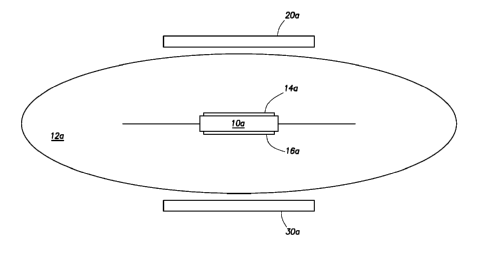
[020] Referring now to Fig. 1A, a device 10a inside a pharmaceutical product
12a, such as a pill or tablet, which is completely packaged up and tested via
a
probe, as discussed in detail below. In accordance with various aspects of the
present invention, the device 10a may be located within the product 12a or
secured to the surface of the product 12a, as contemplated within the scope of
the present invention. The device 10a includes a control module for
communication and a memory for storing information, such as identity. The
probing of the device 10a is performed to ensure, for example, that the device
10a is still functioning. The probing uses a capacitive coupling approach
where
there is capacitive coupling of a first probing capacitive plate 20a to a
first metal
or material 14a on one side of the device 10a and a second probing capacitive
plate 30a to a second metal or material 16a on another side of the device 10a.
As evident to one skilled in the art, the plate 20a is electrically insulated
from the
plate 30a even though the insulation is not specifically shown. Various ways
to
probe using capacitive coupling may be accomplished, e.g., metal, metal pads,
etc. In accordance with one aspect of the present invention, for example,
there is
capacitive coupling between material 14a and capacitive plate 20a and material
16a and capacitive plate 30a. The plates 20a and 30a are probes that can
communicate with the device 10a through capacitive coupling. The plates 20a
and 30a are electrically connected to a system (not shown) that can receive
the
information from the plates 20a and 30a as well as process the information.
Also, in accordance with various aspects of the present invention, the product
may be coated with non-conducting material.
[021] In accordance with various aspects of the present invention, there are
various components included as part of the device 10. For example, the device
may be an ingestible event marker (IEM) with a unique identity that can be
read using capacitive coupling pre-ingenstion and communicated using
transconduction post-consumption. Various aspects of an IEM are disclosed in
US Patent Application 12/564,017 titled COMMUNICATION SYSTEM WITH
PARTIAL POWER SOURCE filed on September 21, 2009.
4
CA 02780361 2012-05-08
WO 2011/057024 PCT/US2010/055522
[022] Referring now to Fig. 1B, a device 10b is shown as part of a product 12b
in
accordance with one aspect of the present invention. The device 10b includes a
first
material 14b and a second material 16b deposited on the surface of the device
10b for
forming a capacitive connection. The materials 14b and 16b are in
communication with
the control module of the device 10b. Probes 20b and 30b are capacitively
coupled to
materials 14b and 16b, respectively. Thus, as the probes 20b and 30b are
powered up
with AC voltage, then materials 14b and 16b are capacitively coupled to the
probes 20b
and 30b. Thus, information associated with the device 10b that is stored in
the memory
of the device 10b can be encoded by a control module of the device 10b and
communicated to the probes using capacitive coupling.
[023] Referring now to Fig. 1C, a device 10c is shown secured to a product 12c
in
accordance with the present invention. The device 10c includes a first
material 14c and
a second material 16c deposited around the perimeter of a skirt 18c of the
device 10c
with at least a portion of the materials 14c and 16c being deposited on the
skirt 18c.
Furthermore, the materials 14c and 16c are coupled to the control module of
the device
10c to allow for communication through capacitive coupling from the control
module of
the device 10c to allow the identity of the device 10c to be communicated to a
system
through the probes 20c and 30c. In accordance with one aspect of the present
invention, the materials 14c and 16c are conductive inks, such as an
ingestible graphite
or carbon based ink or paste. Probes 20c and 30c are powered by an AC source
and
when brought close to the materials 14c and 16c, the probes 20c and 30c can
communicate with the device 10c using capacitive coupling through the
materials 14c
and 16c, respectively. Furthermore, in accordance with another aspect of the
present
invention, probes 22c and 32c are positioned proximal to the material 14c and
16c at
different locations to allow for alternative positioning of the device 10c or
to provide for
probing of the device from an alternative direction. Once the probes 20c and
30c are
powered with an AC voltage and the device 10c is located near the probes 20c
and 30c,
then the materials 14c and 16c can be used to pass information between the
device 10c
and the system connected to the probes 20c and 30c through capacitive
coupling.
[024] Referring now to Fig. 1D, a device 10d is shown in accordance with
another
aspect of the present invention. A conducting material 14d is deposited on the
surface
CA 02780361 2012-05-08
WO 2011/057024 PCT/US2010/055522
of a material 19a that is associated with the device 10d. The material 19a and
the
material 19b of the device 10d are dissimilar materials and form a partial
power source
for the device 10d. For example, the material 19a maybe CuCI and the material
19b
may be Mg. The device 10d also includes transistors at connection 19c that is
capable
of electrically connected the composite 14d to V-high or the material 19b,
which is at the
same potential as V-low. The device 10d includes a composite material 16d that
is
physically associated with the device 10d and rests on top of an oxide layer
17d. The
material 16d may be gold-plated CuCl. Thus, as probes or plates, similar to
those
shown in Figs. 1A-1C and powered by an oscillating or AC voltage source, are
brought
close to the device 10d there is capacitive coupling between the composite 14d
and the
composite 16d and the probes. In accordance with one aspect of the present
invention,
as the voltage source isolates, the energy transferred to the material 14d and
the
material 16d varies accordingly and is stored on the device 10d. As the
voltage source
is reduce to zero or quiet, then the device 10d switches from receiving energy
to
sending energy to the probes using capacitive coupling. In order to creating
an
oscillating energy source, the transistors 19c are used to connect and
disconnect the
material 14d between the material 19b (which represents V-low) and V-high. As
the
material 14d changes energy levels from V-high to V-low, information can be
transferred
to the probes. Thus, during a portion of the cycle when the power is off or
quiet (as
shown in Fig. 2C), the device 10d is able to transfer energy to the probes,
which energy
includes information about the device 10d. Hence, using capacitive coupling,
information may be communicated between the device 10d and the system
connected
to the probes near the device 10d.
[025] Referring now to Fig. 1E, a co-axial probe with two conductive
probes/plates 20e
and 30e separated by an insulating material 25e. The inner conductive probe or
plate
20e is surrounded by the insulating material 25e, which is surrounded by the
outer
conductive probe or plate 30e. The device 10e is shown as part of a
pharmaceutical
product 12e. The device 10e includes a conducting material or ink 15e
deposited on
the side opposite the co-axial probe. As the co-axial probe is positioned
close to the
product 12e, the probe 20e is positioned over the center of the device 10e and
the
probe 30e is positioned above the outer edges of the device 10e and proximal
to the
6
CA 02780361 2012-05-08
WO 2011/057024 PCT/US2010/055522
material 15e. Thus, as described above and with respect to Fig. 20, as the
power
source is isolating, energy is transferred from the co-axial probe to the
device 10e and
as the power source is shut-off or quiet, then energy is transferred from the
device 10e
to the system connected to the co-axial probe.
[026] Referring now to Fig. 2, a voltage source, e.g., an AC voltage or other
isolating
or alternating source 40 runs at a high frequency, e.g., 1 MHz, etc. The
voltage source
is connected to the probes or plates. The device 10 includes a control module
50 and
bonding pads 52 to which the materials (for example, materials 14 and 16 of
Fig. 1A)
are coupled. In accordance with one aspect of the present invention, inside
the device
is a diode 54, such as a Schottky diode or other type of diode that creates an
internal
supply voltage, and a switch 56 with some impedance that is turned on and off
which
changes the impedance of the device 10. The variation in the impedance is used
to
communicate information about the identity of the device 10. The change in
impedance
allows for the information associated with the device 10 to be encoded and
sent to a
system through the probes using capacity coupling, as represented by the
capacitors 58
and 60. The information is captured by the system connected to the probes
represented by the capacitors and read as Vout through the sampling amplifier
across
the impedance labeled R-sample.
[027] Once the control module 50 is brought near or exposed to the voltage
source
through the plates, there is energy transfer through the capacitive coupling
and the
device 10 can produce an oscillation signal, which can be detected. The
oscillation
signal contains information and the isolating signal can be encoded into, for
example, a
1 MHz signal or similar frequency, e.g., 500 KHz, as may be dependent on the
degree
of capacitive coupling. The voltage of the source 40 will be determined by how
much
capacitive coupling is achieved between the capacitive plate or probe 20 and
30 of Fig.
1 and the materials 14 and 16 thereof. Thus, at a high frequency that
represents,
perhaps, 5 volts, the capacitive value between the probe, such as probe 20 or
30, and
the material is represented by the capacitors 58 and 60.
[028] Referring now to Fig. 2A and 2B, in accordance with another aspect of
the
present invention, a diode bridge is shown that is a circuit representation of
the
interaction between the plates 20 and 30 and the materials 14 and 16 of the
device 10.
7
CA 02780361 2012-05-08
WO 2011/057024 PCT/US2010/055522
The isolating voltage present at the plates 20 and 30 (labeled "PLATE 1" and
"PLATE
2") results in an energy transfer in the form of high voltage and a low
voltage for the
device 10. The device 10 includes a control module as part of the processor or
logic
unit. The logic unit may be a processor, a microprocessor, a multi-module
device or
any form of integrated circuit. The logic unit is in communication with the
conductive
materials 14 and 16 and the plates 20 and 30 (labeled "PLATE 1" and "PLATE
2"). As
the plates 20 and 30 are powered with an AC source, the logic unit stores
energy and
later uses that energy to send information.
[029] Referring now to Fig. 2C, the power cycle is shown with an active period
and a
quiet period and the transfer cycle of the device 10 is shown as the transfer
window. In
accordance with the present invention, the duration of the active period
energy is
transferred from the power source to the device 10. Then during the quiet
phase, the
energy stored by the device 10 is used to transfer energy from the device 10
to the
system connected to the probes. In this way, information associated with the
device
can be transferred from the device 10 through the probes 20 and 30 to the
system
connected to the probes. In accordance with various aspects of the present
invention,
the information sent from the device 10 to the system of the probes 20 and 30
during
the quiet phase is based on the information stored in memory of the device.
Thus, even
though there is a "1" shown during the transfer window or quiet stage of the
power
source, the information transferred during the quiet stage or phase of the
power source
may be a "0".
[030] In accordance with one aspect of the present invention, if there is a
one-
microfarad capacitor between a capacitive plate/probe and a material
physically
associated with the device 10, then at a high isolating frequency that
represents a lower
voltage necessary for capacitive coupling. In accordance with another aspect
of the
present invention, if there is a one-picofarad capacitor, then a larger
voltage may be
needed, as will be recognized by one skilled in the art. The amount of current
actually
going through will depend on the impedance between the electrical circuit
caused
between the capacitive plates/probes 20 and 30, as shown in Fig. 1 for
example. Thus
shorting capacitive plate 20 and capacitive plate 30 of Figs. 1A-1C will
result in
significant current going through which may be detected with, for example, by
a
8
CA 02780361 2012-05-08
WO 2011/057024 PCT/US2010/055522
sampling amplifier as shown in Fig. 2. The output is through a sampling
amplifier which
is essentially looking at the current going through the loop and the
modulation of that
current caused by the control module 50.
[031] In accordance to various aspects of the present invention, the
capacitive coupling
may be used with devices that are DC source devices, which are modified for
interoperability, e.g., a device having a rectifier in place to provide a
stable voltage on
the chip, the impedance of which may be modulated.
[032] Referring now to Figs. 3A and 3B, in accordance with various aspects of
the
present invention, the capacitive plates/probes and the system connected
thereto for
receiving information may be integrated or otherwise associated with various
structural
components and other devices, e.g., a tubular structure 60 as shown in Fig. 3A
having
capacitive plates 20 and 30. To illustrate, one or more pharmaceuticals having
an IEM
or similar device 10 may be introduced into the structure. The device 10 may
be
introduced manually or automatically via automated means. As the device
travels
through the structure 60, the device 10 is probed by the capacitive plates 20
and 30 in
the tube 60. In various aspects, other devices and/or components may be
associated.
In one example, a programmable device may be communicatively associated with
the
capacitive coupling device to receive and/or transmit data and/or information
derived by
the capacitive coupling device. To continue with the foregoing illustration,
once all or a
portion of the number of products 10, which may be pills, are probed or "read"
by the
capacitive coupling system associated with the probes/plates 20 and 30, the
capacitive
coupling system can communicate, e.g., wireless, wired, etc., to a database
with a
display device for further storage, display, manipulation, etc. In this
manner, an
individual datum, data, large volumes of data, etc., may be processed for
various
purposes. One such purpose may be, for example, to track pharmaceuticals in a
supply
chain application, e.g., during a manufacturing process such as a tablet
pressing or
other process, during a pharmacy verification process, during a pharmacy
prescription
process, etc. Various processes may be complementary, incorporated, etc. One
such
example is validation through reading the number. If it is valid, e.g.,
readable, the tablet
is accepted. If not, the tablet is rejected. Thus, using a simple hand held
reader with an
oscillating power source, a user or care provider can probe the product, which
can be a
9
CA 02780361 2012-05-08
WO 2011/057024 PCT/US2010/055522
pill or tablet in accordance with one aspect of the present invention, with
the device 10
associated therewith and determine if the pill is authentic or a counterfeit
product.
[033] Referring now to Figs. 4A and 4B, in accordance with another aspect of
the
present invention, a pill having a device 10 is shown with a coating 74 that
is non-
conductive or fairly impervious coating and the pill itself comprises a non-
conductive
medicine powder. A region 72, e.g., a cone-shaped region, as shown, comprises
a
conductive material 70, e.g., small particles or grains of conductive material
intermixed
with other pharmaceutical material(s), excipient(s), placebo material(s),
etc., such that
the region 72 is converted into a conductive region. For example, graphite and
other
conductive materials may be used, e.g., one part in ten, five parts in ten,
etc. such that
the region 72 is conductive. Other materials and compositions are possible,
e.g., a gel
or liquid capsule having conductive particles therein, etc.
Thus, at high enough
frequencies, the particles of the conductive material 70 in the region 72 may
be shorted
together. One
skilled in the art will recognize that the conductive material 70 may
include various materials and form factors, as well as combinations thereof,
e.g.,
variously sized particles, wires, metal films, threads, etc. The scope of the
present
invention is not limited by the type or shape of the conductive material 70
used in the
region 72.
[034] In accordance with another aspect of the present invention, the
conductive
material 70 may be integrated or formed via a variety of methods and
proportions. In
one example, the device 10 is embedded or otherwise mechanically associated
with a
"doughnut-shaped" powder and the hole formed therein is filled or otherwise
associated
with the conductive particles, etc., to form the conductive region. The
size, area,
volume, locations or other parameters of the conductive regions may vary to
the extent
the functionality described herein may be carried out.
[035] In accordance with another aspect of the present invention and as shown
in
Figure 5, capacitive plates or probes 80 and 82 are coupled to a system for
collecting
the data. Probes 80 and 82 are used to probe the device 10 through capacitive
coupling to the materials 84 and 86, respectively. An impedance feedback
system may
be used to drive them fairly close to one another and once the current gets to
a certain
amount to use that to gauge the distance. Using a high enough impedance, this
system
CA 02780361 2012-05-08
WO 2011/057024 PCT/US2010/055522
may be useful in a variety of applications, e.g., a manufacturing environment
to validate
that the device 10 is present, is operating correctly etc.
[036] In accordance with another aspect of the present invention, a close
proximity
between the capacitive coupling probes/plates and the device 10 may
facilitate,
promote, etc., privacy aspects. In certain aspects, certain related devices
may include,
for example, a circuit with a Schottky diode in parallel with a CMOS
transistor that is
timed to be opened and closed, opened up, etc. Other circuit designs and
modifications
are possible.
11