Note: Descriptions are shown in the official language in which they were submitted.
CA 02781432 2012-05-17
WO 2011/066396 PCT/US2010/058015
1
DESCRIPTION
METHOD AND APPARATUS FOR SENSING INFRARED RADIATION
CROSS REFERENCE TO RELATED APPLICATION
The present application claims the benefit of U.S. Provisional Application
Serial No.
61/264,071, filed November 24, 2009, which is hereby incorporated by reference
herein in its
entirety, including any figures, tables, or drawings.
BACKGROUND OF INVENTION
Existing night vision goggles require very high operating voltages and cost
thousands
of dollars. Typical night vision goggles are complex electro-optical devices
that intensify
existing light instead of relying on their own light source. Night vision
goggles can be
sensitive to a broad spectrum of light, from visible through infrared. In a
typical
configuration, a conventional lens, called the objective lens, captures
ambient light and some
near-infrared light. The gathered light is then sent to an image-intensifier
tube. The tube
outputs a high voltage, typically about 5,000 volts, to the tube components.
The image-
intensifier tube can use a photo cathode to convert the photons of light
energy into electrons.
As the electrons pass through the tube, more electrons can be released from
atoms in the tube,
multiplying the original number of electrons by a factor of thousands. One
method to
accomplish this multiplication is through the use of a micro channel plate
(MCP). The MCP
is positioned in the tube such that when the electrons from the photo cathode
hit the first
electrode of the MCP, they can be accelerated into the glass micro channels by
high voltage
(about 5,000 Volts) bursts being sent between the electrodes of the electrode
pair. As
electrons pass through the micro channels, they cause other electrons to be
released in each
channel using a process called cascaded secondary emission. These new
electrons can also
collide with other atoms, creating a chain reaction that can result in
thousands of electrons
leaving the channel where only a few entered.
The image-intensifier tube can be positioned so that at the end of the tube,
the
cascaded electrons hit a screen coated with phosphors. These electrons
maintain their
position in relation to the channel they passed through. The energy of the
electrons causes
the phosphors to reach an excited state and release photons. These phosphors
create the
CA 02781432 2012-05-17
WO 2011/066396 PCT/US2010/058015
2
green image on the screen that has cone to characterize night vision. Since
the electrons stay
in the same alignment as the original photons, a reliable image can be
produced. The green
phosphor image can be viewed through another lens, called the ocular lens that
allows you to
magnify and focus the image. The night vision device can be connected to an
electronic
display, such as a monitor, or the image can be viewed directly through the
ocular lens.
Recently, light up-conversion devices have attracted a great deal of research
interest
because of their potential applications in night vision, range finding, and
security, as well as
semiconductor wafer inspections. Early near infrared (NIR) up-conversion
devices were
mostly based on the heterojunction structure of inorganic semiconductors.
These devices
consist of two parts in series: one part for photodetection and another for
luminescence. The
up-conversion devices are mainly distinguished by the method of
photodetection. However,
the up-conversion efficiencies of recent devices continue to be very low. For
example, one
NIR-to-visible light up-conversion device that integrates a light-emitting
diode (LED) with a
semiconductor based photodetector has only exhibited a maximum external
conversion
efficiency of 0.048 (4.8%) W/W. Even a hybrid organic/inorganic up-conversion
device that
integrates an inorganic InGaAs/inP photodetector with an organic light-
emitting diode
(OLED) only exhibits an external conversion efficiency of 0.7% W/W. In
addition, current
inorganic and hybrid up-conversion devices are expensive to fabricate and the
processes used
for fabricating these devices are not compatible with large area applications.
BRIEF SUMMARY
Embodiments of the invention pertain to a method and apparatus for sensing
infrared
(IR) radiation. Specific embodiments for sensing IR radiation provide improved
dark current
characteristics. An embodiment can incorporate an all-organic device. In one
embodiment,
an all-organic up-conversion device is provided that can be fabricated by
integrating an
organic light emitting device (OLED) and an organic photodetector into one
device. An IR
sensing layer of an OLED in accordance with an embodiment of the invention can
be formed
of a poor hole transporting layer. In certain embodiments, the IR sensing
layer can be
incorporated with an OLED to provide IR-to-visible color up-conversion.
In a specific embodiment, a night vision device can be fabricated by
depositing a few
layers of organic thin films. Embodiments of the subject device can operate at
voltages in the
range of 10-15 Volts and have lower manufacturing costs compared to
conventional night
CA 02781432 2012-05-17
WO 2011/066396 PCT/US2010/058015
3
vision devices. Embodiments of the device can incorporate an organic
phototransistor in
series with an organic light emitting device. In a specific embodiment, all
electrodes are
transparent to infrared light.
BRIEF DESCRIPTION OF DRAWINGS
Figure 1 shows an energy band diagram of an infrared sensing up-conversion
device
in accordance with an embodiment of the subject invention.
Figure 2 shows a device structure in accordance with an embodiment of the
subject
invention that allows an electron to generate multiple photons.
Figure 3 shows the operation of an up-conversion device in accordance with an
embodiment of the subject invention.
Figure 4 shows an energy band diagram of another infrared sensing up-
conversion
device in accordance with an embodiment of the subject invention.
Figure 5 shows a structural diagram of the device of Figure 4.
Figures 6A and 6B show the light-current-voltage characteristics of the device
of
Figure 4, where Figure 6A shows the characteristics when the device is dark
and Figure 6B
shows the characteristics when the device is exposed to infrared radiation.
Figures 7A and 7B show the current efficiency of a control organic light
emitting
device (Figure 7A) and the device of Figure 4 (Figure 7B).
Figure 8A shows the absorbance spectra of a 100 nm thick neat SnPe film and a
100
nm thick SnPe:C60 mixed film in accordance with an embodiment of the subject
invention.
Figure 8B shows the dark I-V characteristics of the control OLED (shown in the
inset
of Figure 7A) and two up-conversion devices in accordance with embodiments of
the subject
invention, where one device has a 100 nm thick neat SnPc film and the other
device has a 100
nm thick SnPe:C60 mixed film.
Figure 9A shows light-current-voltage characteristics of an infrared-to-green
light up-
conversion device according to an embodiment of the subject invention under
dark and photo
(infrared) irradiation.
Figure 9B shows a plot of the on/off ratio as a function of current densities
for an
infrared-to-green light up-conversion device in accordance with an embodiment
of the
subject invention.
CA 02781432 2012-05-17
WO 2011/066396 PCT/US2010/058015
4
Figures 10A and 10B show the photon-to-photon conversion efficiency of the
device
of Figure 5 (Figure 11 A) and the quantum efficiency of another embodiment of
the subject
invention (Figure 11 B).
DETAILED DISCLOSURE
Embodiments of the invention pertain to a method and apparatus for sensing
infrared
(IR) radiation. An embodiment of the present invention provides an all-organic
up-
conversion device that can be fabricated by integrating an OLED and an organic
photodetector into one device. Because of their compatibility with
lightweight, rugged, or
flexible plastic substrates, all organic up-conversion devices in accordance
with embodiments
of the present invention can be used for numerous applications including, but
not limited to,
night vision, range finding, security, and semiconductor wafer inspections.
In a specific embodiment, a night vision device can be fabricated by
depositing a few
layers of organic thin films. Embodiments of the subject device can operate at
voltages in the
range of 10-15 Volts and have lower manufacturing costs compared to
conventional night
vision devices. In a specific embodiment, all electrodes are transparent to
infrared light.
The wavelength of the imaging device for thermal imaging can be adjusted by
material selection. In a particular embodiment, the imaging device includes an
infrared
absorbing layer that has 3 layers, which are IR sensitive. An embodiment can
incorporate a
tandem light emitting device (LED) including multiple LED's in a stack. In a
particular
embodiment, one photon enters the imaging device and passes through five LED's
in a stack,
generating five photons as output. The five LED's stacked together uses a
higher voltage
than a single LED, but can still allow the device to operate at a low voltage.
The five stacked
LED's can also make the imaging device thicker than a device with a single LED
and,
therefore, less sensitive to noise.
Figure 1 shows an energy band diagram of an IR sensing up-conversion device
which
can be incorporated in an embodiment of the subject invention.
Embodiments of an IR sensing device, such as the device shown in Figure 1, in
accordance with the subject invention can have two parts, an IR sensitizer, or
IR sensing
layer, and a light emitting device. In an embodiment, the maximum quantum
efficiency of
the device shown in Figure 1 is 100%. In an embodiment of the invention, in
order to
enhance performance, the device is fabricated with a tandem structure.
CA 02781432 2012-05-17
WO 2011/066396 PCT/US2010/058015
Figure 2 shows a device having such a tandem structure, incorporating an IR
sensing
layer and an LED, in accordance with an embodiment of the subject invention.
With this
structure, one electron can generate multiple photons. Incorporating this
device architecture,
the output of the device can be enhanced to achieve gain. Due to the increase
thickness of the
device, the dark current can be lowered and the device performance
substantially improved.
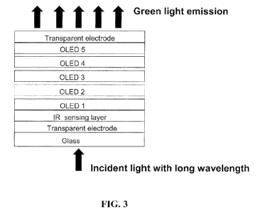
Figure 3 shows the operation of an up-conversion device in accordance with an
embodiment of the subject invention. As shown, light with an IR wavelength can
enter the
device through a transparent or semi-transparent substrate, such as glass or
other appropriate
transparent or semi-transparent material. A photon can then pass through a
first transparent
(or semi-transparent) electrode and strike an IR sensing layer. The IR sensing
layer can be
sensitive for the range 0.8 .im-2 m in a specific embodiment. In further
specific
embodiments, the IR sensing layer can be sensitive to wavelengths in the range
of 700 nm to
14 m, in the range of 1 tm to 4 m, and in the range of 1 ~tm to 3 m. The IR
sensing layer
can then produce carriers, such as electrons and holes, such that the
electrons, or holes, are
passed to a stack of LEDs. In Figure 3, organic light emitting devices (OLEDs)
are shown
but other light emitting devices can be used with the subject invention. In a
particular
embodiment the LEDs are transparent or semi-transparent. When the carriers,
such as
electrons, from the IR sensing layer enters the first LED (OLED in Figure 3)
and combine
with corresponding carriers, such as holes, a photon can be generated and
passed through the
device. In the charge separation layer between the first and second LED (OLED
1 and
OLED 2 in Figure 3) an electron and a hole are generated, such that the hole
can enter the
first LED and combine with an electron entering the first LED from the IR
sensing layer to
produce a photon. Here, five LEDs are shown in series, therefore five photons
can be
generated for each photon which enters the device. The LEDs can be identical
or can be
different. As discussed below, the LEDs can be produced as thin films.
Therefore, multiple
LEDs can be stacked without producing an unwieldy device. In a particular
embodiment,
three to eight LEDs can be stacked in series. In further embodiments, more
LEDs can be
stacked. As additional LEDs are stacked, noise can be reduced even if the gain
is not as high.
Referring to Figure 3, in a specific embodiment, a hole blocking layer (not
shown in
Figure 3) can be added between the transparent electrode the IR radiation
enters and the IR
sensing layer. Such a layer can block holes from passing from the transparent
electrode to
the IR sensing layer and/or from the IR sensing layer to the transparent
electrode. Specific
CA 02781432 2012-05-17
WO 2011/066396 PCT/US2010/058015
6
embodiments incorporating such a hole blocking layer can utilize ZnO
nanoparticles, Ti02
nanoparticles, or other appropriate materials known in the art. The ZnO
nanoparticles or
Ti02 particles, and/or a ZnO layer or TiO2 layer, can be deposited on the
transparent
electrode prior to adding the 1R sensing layer.
As shown in Figure 3, in a specific embodiment a second transparent (or semi-
transparent) electrode, or cathode, can be disposed on the other side of the
LED stack. In this
embodiment, a potential between the pair of electrodes can drive the carriers,
such as holes,
from the IR sensing layer into the first LED and holes from each charge
separation layer,
where electrons and holes are generated, into the LED toward the cathode
electrode.
Likewise, electrons injected by the cathode are driven into the fifth LED and
the electrons
generated in the charge separation (generation) layers are driven into the LED
toward the
anode.
Transparent electrodes can be produced by replacing reflective electrode
materials
(such as aluminum) with transparent materials (such as indium-tin oxide). In
one
embodiment of the subject invention, a layered CsCO3 (I nm)/Ag (10 nm)/ITO
(100 nm)
electrode is used as the top electrode. The CsCO3 interlayer lowers the
cathode work-
function to match the conduction (LUMO) energy of Phenyl-C61-Butyric-Acid-
Methyl-Ester
(PCBM), a material that can be used as part of the OLED. The thin Ag layer
provides
conductivity and the ITO layer provides encapsulation. Embodiments of this
thin film stack
have a 90% optical transmission and sheet resistance less than 5 ohm/sq, which
is 70% lower
than typical ITO electrodes. In a specific embodiment, a thin film of MgAg or
ITO can be
utilized as a transparent electrode, for example a transparent electrode in
contact with the last
light emitting device. The thin film can be 20 mn thick or less in a specific
embodiment.
OLEDs can be produced that generate any wavelength of visible light. In one
embodiment, an organic emissive layer includes three different dye molecules
emitting blue,
green, and red lights, respectively. By controlling the relative abundance of
the three dye
molecules in the device, white light with high color rendering index >90 can
be achieved. In
another embodiment, different colors are achieved by varying the relative
abundance of the
three dye molecules or by varying the power transmitted to the different
molecules.
For transparent OLEDs, a transparent material (such as indium-tin oxide) can
again be
used as the cathode. In this way, photons can pass through the stacked OLEDs.
The organic
materials used in these devices are mostly transparent in the visible spectrum
due to the high
CA 02781432 2012-05-17
WO 2011/066396 PCT/US2010/058015
7
band gap of these materials (typically > 3 eV). Exceptions can include the dye
molecules
from which the desired light emission is generated; however, the dye molecules
can be
incorporated as dopants (typical doping concentrations -1-10 wt%) in the
emissive layer
whose thickness is typically 10-30 nm. Therefore, the entire OLED device can
achieve a
very high transparency of 90% or higher.
In fabricating transparent OLEDs with triple-doped organic emissive layers,
the
damage to the underlying organic layers can be minimized during the sputter
deposition of
the indium-tin oxide transparent cathode. In addition, low sheet resistance,
and high
transparency can be obtained for the transparent electrode, and efficient
charge injection at
the electrode/organic interface can be achieved. As discussed above, a
composite electrode
of C5CO3/Ag/ITO can also be used as the transparent electrode for the OLEDs.
Furthermore,
a microlens array can also be fabricated on the substrate surface to enhance
the extraction of
light in that direction. Moreover, OLEDs can be produced that offer high
quality lighting
with a color rendering index larger than 90.
In a further embodiment, the electrodes and LEDs used are transmissive for
some
wavelengths of light and absorb other wavelengths.
According to certain embodiments, the light sensing layer can incorporate
quantum
dots such as PbSe and PbS quantum dots.
In a particular embodiment, the subject up-conversion devices can be
incorporated
into night vision goggles or other light amplifying devices. In a further
embodiment, green
OLEDs are used so that a green amplified image as produced as with
conventional night
vision goggles.
Figure 4 shows an energy band diagram of another IR sensing up-conversion
device
in accordance with an embodiment of the subject invention. According to an
embodiment, a
poor hole injection and transport layer can be incorporated in the IR sensing
up-conversion
device to improve dark current characteristics. In specific embodiments, in
order to reduce
dark currents and, therefore, improve SNR, a material can be chosen for the
hole injection
and transport layer that has a current density of less than 1 mA/cm2. In less
preferred
embodiments, materials with current densities greater than or equal to 1
mA/em2 can be used
for the hole injection and transport layer, which would increase the injection
of holes from
the electrode when a voltage is applied so as to increase the dark current and
reduce SNR. In
one embodiment, a SnPc:C60 mixed layer, which exhibits poor hole injection and
hole
CA 02781432 2012-05-17
WO 2011/066396 PCT/US2010/058015
8
transport, allows the device to have a low dark current without IR
irradiation. In this
embodiment, the OLED can be essentially turned-off when it is not exposed to
IR radiation.
Figure 5 shows a structural diagram of the device of Figure 4.
Referring to Figure 5, an organic near infrared (NIR)-to-visible up-conversion
device
can be provided using a tin phthalocyanine (SnPc):C60 bulk heterostructure
layer as a NIR
sensitizer and a fac-tris(2phenylpyridinato) iridium (III) (lrppy3) layer as a
phosphorescent
emitter. By using a phosphorescent emitter, light generation can be
accomplished using low
energy, providing an energy-efficient OLED. As one difference from a
conventional OLED
structure, the up-conversion device according to an embodiment of the present
invention
incorporates a poor hole transport NIR-sensitizing layer to keep the device in
the off-state in
the absence of IR irradiation. Upon photo-excitation, the photo-generated
holes are injected
into the OLED and recombine with electrons injected from the cathode to give
off visible
light.
Figures 6A and 6B show the light-current-voltage (L-I-V) characteristics of
the device
of Figure 5. CuPe: ph = 7 x 1.0-4 emz/Vs. SnPc: i, = 2 x 10⁻¹⁰ cm2/Vs. Figure
6A shows the
characteristics when the device is not exposed to any infrared light. The open
circle is current
density and the closed circle is luminescence. As shown, in this embodiment,
without
infrared light irradiation, emission was not observed until 13 V. As discussed
above, the high
turn-on voltage in this embodiment is due to the poor hole injection from the
SnPc:C60 layer.
Figure 6B shows the characteristics when the device is exposed to IR
radiation. An
830 rim laser with 14 mW/em2 was used to irradiate the device. As shown, in
this
embodiment, the OLED was turned on at 2.7 V with infrared illumination from
the laser.
The maximum on/off ratio exceeded 1400 at 12.7 V.
Figures 7A and 7B show the current efficiency of a control organic light
emitting
device (Figure 7A) and the device of Figure 4 (Figure 7B). As shown, in this
embodiment,
the current efficiency under IR illumination is more than 100 cd/A. The higher
current
efficiency indicates that the control OLED is still charge imbalaneed and
slightly electron
dominant.
According to certain embodiments of the present invention, a SnPc:C60 bulk
heterostructure layer is used for the poor hole transport IR sensitizing layer
because of its
strong IR absorption, as shown in Figure 8A, and its poor hole transport
property, as shown
in Figure 8B. Figure 8B shows the dark current-voltage (I-V) characteristics
of the control
CA 02781432 2012-05-17
WO 2011/066396 PCT/US2010/058015
9
OLED (see inset of Figure 7A) and up-conversion devices with NIR sensitizing
layers in
accordance with embodiments of the present invention. The addition of the neat
SnPc layer
increases the turn-on voltage from 3 V to about 5 V and the operating voltages
across the
measurement range also increases by about 2 V, indicating the poor hole
transport properties
of SnPc. The addition of the SnPc:C60 mixed film further increases the
operation voltage by
another 2 V. Compared with the controlled OLED device, the up-conversion
device with the
SnPc:C60 mixed layer shows a significant reduction of hole current.
Figure 9A shows the luminescence-current-voltage (L-I-V) characteristics of
the NIR-
to-green up-conversion device with the SnPc:C60 mixed film as a poor hole
transport NIR-
sensitizing layer according to an embodiment of the present invention. Without
infrared light
irradiation, emission was not detected until the voltage reaches 13 V, showing
the maximum
luminance (1 cd/m2) at 15 V. The high turn-on voltage indicates the poor hole
transport from
the SnPc:C60 mixed layer. The current may be dominated by electrons injected
from the
cathode contact. Upon irradiation with NIR light, the device was turned on at
2.7 V along
with on an onset of green light emission, showing a luminance of 853 cd/m2 at
15 V.
Therefore, the switching effect by IR light is significant as shown in Figure
9B, which
provides the on/off ratio at different voltages. As shown, the maximum on/off
ratio of
luminescence intensity was about 1400 at 12.7 V.
Figures 1OA and 10B show the photon-to-photon conversion efficiency of the
device
of Figure 4 (Figure IOA) and the quantum efficiency (QE) of another embodiment
of the
subject invention (Figure IOB).
The photon-to-photon conversion efficiency (iy0on)from incident IR light
photons to
emitted green light photons can be calculated by the following equation:
lliphoto (a) dx
#of photon extracted J JR(li)hc
#of photon injected )-lRPIR
he
where h is Planks constant, c is the speed of light, 2 is the photon
wavelength, 'photo is the
photocurrent, f is the fraction of photons reaching the sensitizing layer,
R(?) is the
responsivity of the photodetector, a,,R is the incident infrared wavelength,
and PIR is the
incident infrared power.
Again, an 830 nm laser with 14 mW/cm 2 was used to irradiate the device. As
shown,
for the device of Figure 4, the photon-to-photon conversion efficiency
increases as the
CA 02781432 2012-05-17
WO 2011/066396 PCT/US2010/058015
applied voltage increases, and the photon-to-photon conversion efficiency was
2.7% at 15 V.
This up-conversion efficiency is significantly higher than the efficiencies of
previously
demonstrated all-organic up-conversion devices using the fluorescent OLED.
In the up-conversion device structure for the measurements, as shown in the
inset of
Figure 10B, the whole photodetector structure is not used. Rather, the IR
absorbing layer is
used as the hole injection layer. Therefore, the exact external quantum
efficiency is not
measured from injecting IR light to extracting charge carriers. However, the
external
quantum efficiency is measured indirectly by making this photodetector
structure. In the up-
conversion device shown in the inset of Figure 10B, a 20 nm thick SnPc:C60
mixed layer is
used alone, and the 830 nm IR laser with 14 mW/cm2 is used for the IR source.
In a same IR.
irradiation and same IR absorbing layer thickness, 5.20% external quantum
efficiency (EQE)
was obtained.
The EQE of the Irppy3 based OLED is roughly 20% in the literature. Therefore,
the
calculated conversion efficiency is about 1-4% and it is consistent with the
experimental
conversion efficiency. This conversion efficiency is roughly 10 times higher
than that of the
red-to-green up-conversion devices.
Any reference in this specification to "one embodiment," "an embodiment,"
"example
embodiment," etc., means that a particular feature, structure, or
characteristic described in
connection with the embodiment is included in at least one embodiment of the
invention. The
appearances of such phrases in various places in the specification are not
necessarily all
referring to the same embodiment. Further, when a particular feature,
structure, or
characteristic is described in connection with any embodiment, it is submitted
that it is within
the purview of one skilled in the art to utilize or combine such feature,
structure, or
characteristic in connection with other ones of the embodiments.
It is to be understood that the figures and descriptions of embodiments of the
present
invention have been simplified to illustrate elements that are relevant for a
clear
understanding of the invention, while eliminating, for purposes of clarity,
other elements that
may be well known. Those of ordinary skill in the art will recognize that
other elements may
be desirable and/or required in order to implement the present invention.
However, because
such elements are well known in the art, and because they do not facilitate a
better
understanding of the present invention, a discussion of such elements is not
provided herein.
CA 02781432 2012-05-17
WO 2011/066396 PCT/US2010/058015
11
A greater understanding of the present invention and of its many advantages
may be
had from the foregoing examples, given by way of illustration. The foregoing
examples are
illustrative of some of the methods, applications, embodiments and variants of
the present
invention. They are, of course, not to be considered in any way limitative of
the invention.
Numerous changes and modifications can be made with respect to the invention.
All patents, patent applications, provisional applications, and publications
referred to
or cited herein are incorporated by reference in their entirety, including all
figures and tables,
to the extent they are not inconsistent with the explicit teachings of this
specification.
It should be understood that the examples and embodiments described herein are
for
illustrative purposes only and that various modifications or changes in light
thereof will be
suggested to persons skilled in the art and are to be included within the
spirit and purview of
this application.