Note: Descriptions are shown in the official language in which they were submitted.
CA 02782440 2012-07-05
P42186.501
Radar system with synthetic aperture
The invention relates to a SAR (synthetic aperture radar) system with an
antenna that is
composed of one or several partial antennas, wherein each partial antenna
comprises a
plurality of phase centers and transmit/receive modules assigned thereto and a
signal
processing means for the coherent processing of signals of the radiators.
A SAR system of this type is used, for example, with space-based SAR
instruments. Fig. 1
shows a diagrammatic representation of a planar phased array antenna ANT. The
antenna
ANT comprises by way of example six panels Panl,
Pan6 as partial antennas with
respectively 56 radiators Rad as phase centers and a corresponding number of
transmit/receive modules TRM. Electronic components of the antenna ANT, in
particular
components for digital beam forming (DBF), are not illustrated. Each of the
panels Pan l,
Pan6 in the exemplary embodiment is composed of two radiators Rad in the
horizontal
direction (typically in the direction of flight) and 28 horizontal radiator
pairs in the vertical
direction (elevation). In the figure, the horizontal direction runs from left
to right, the vertical
direction runs from top to bottom. The radiators Rad have their feed points
for transmit
signals or receive signals respectively in the center. The already mentioned
transmit/receive
module TRM is arranged behind each of the feed points.
Each transmit/receive unit has on the instrument side an input for a high-
frequency transmit
= signal (HF transmit signal) and an output for a high-frequency receive
signal (HF receive
signal). The HF transmit signal is referred to as a radar transmit pulse, the
HF receive signal
is referred to as a radar echo. In the present specification each
transmit/receive module TRM
represents an individual channel. In principle, several transmit/receive
modules can also be
combined to form a channel. The transmit/receive modules TRM are controlled,
for example,
via electrical line buses ATB and ACB. ATB represents the antenna timing bus,
ACB
represents the antenna control bus. In phased array antennas for SAR systems,
a HF network
for transmit signal distribution and at least one further network for the
receive signal
combination is typically provided on the antenna. Fig. 2 shows in a
diagrammatic
representation the HF network of a typical antenna without digital beam
formation for only
eight radiators Rad. For better clarity, the eight radiators Rad are shown
with vertical spacing
from one another. The transmit/receive modules TRM are coupled to a central
electronic
system COMP. If a signal is to be transmitted by the radiator Rad of the
antenna ANT, this is
{P42186 01469078.DOC}1
CA 02782440 2012-07-05
P42186.S01
fed via an output RF TX as a transmit signal to the transmit/receive modules
TRM. An
analogously combined receive signal of the transmit/receive modules TRM, which
is formed
from the respective signals of the transmit/receive modules TRM of the
radiators Rad, is
digitalized, further processed and finally recorded in the central electronic
system COMP
arranged apart from the antenna. The combined receive signal is fed to the
central electronic
system COMP at an input RF RX.
It is known to use digital beam forming to increase the power of radar
antennas. With SAR
systems this is used, for example, in HRWS (high resolution wide swath)
instruments. One
possible embodiment is described in EP 1 241 487 A1. In digital beam forming,
the receive
signals of all channels (in the exemplary embodiment, all transmit/receive
modules) are
processed before combination. The processing or handling of the receive
signals is usually
carried out digitally. A possible HRWS architecture is shown diagrammatically
in Fig. 3,
wherein the radiators are not shown for reasons of clarity. The analog receive
signals
originating from the transmit/receive modules TRM are respectively digitalized
and
processed in a digital beam fon-ning module DBFM and conveyed as a data stream
data RX
to the central electronic system. The data stream is hereby realized as a
chain, since the signal
combination after the digitalization is a summation. In each beam forming
module DBFM,
the individual signal and the signal of the predecessor in the chain are added
before being
forwarded.
The functions of the beam forming module DBFM comprise a signal filtering, a
down-mixing
of the signal to the baseband, an anti-alias filtering, a digitalization, an
application of the
beam forming algorithms for the current channel on the digital signal, a
coherent, i.e.
synchronous summation of the local signal with that of the preceding signal
and the
forwarding of the sum signal to the next channel, i.e., the forwarding to the
following beam
forming module in the chain. The components FIL, MIX, AAL, ADW and Proc
necessary for
this are shown in Fig. 4 without detailed consideration of an amplifier
arrangement. The
architecture of a single channel is thereby shown without variable damping
elements and
phase control elements. The signal data out resulting at the end is that
signal in the baseband
which a receive antenna would generate with the algorithmically adjusted
receive beam.
The described procedure described in EP 1 241 487 A1 contains the early
digitalization of the
signals already on or at the output of the antenna. As a result, the receive-
side architecture of
{P42186 01469078.DOC}2
the antenna changes fundamentally compared to a classic antenna without beam
formation.
The analog receive network used there is replaced by so-called high-speed
serial links
(HSSL), that is, quick serial data lines. This results from the fact that
large data volumes at a
high data rate have to be transmitted from the antenna to the central
electronic system or
directly to the mass storage device. Depending on the bandwidth of the radar,
data rates per
panel of several 10 Gbps (1 Oxle bits per second) can occur.
This leads to a high implementation expenditure in particular with spaceborne-
capable
components with many parallel lines and considerable data processing
expenditure. For
HRWS instruments with high resolution, very powerful and expensive processing
units, as a
rule FPGAs (field-programmable gate array), have to be used for the data
processing, the
airworthiness of which has not been unreservedly acknowledged. Furthermore,
the high data
rates of the receive chain lead to complex cable runs and high power
consumption. A further
problem of the architecture according to Fig. 3 is the fault dependency of the
components on
one another. A single error in the HSSL data chain brings the function of the
entire panel to a
stop. The architecture in the form shown is therefore not airworthy and
requires a redundancy
concept, which further increases the complexity in the receive chain.
An object of the present invention is to disclose a SAR system with a radar
antenna with
which the signal processing can be carried out in a simpler manner, wherein
the system
should meet the requirement of airworthiness.
The invention creates a SAR system with an antenna that is composed of one or
more partial
antennas, wherein each partial antenna comprises a plurality of phase centers
and
transmit/receive modules assigned thereto as well as a signal processing means
for the
coherent processing of signals of the radiators. According to the invention,
the signal
processing means comprises a hybrid beam forming module for the digitalization
and
processing of the analog receive signals received by the transmit/receive
modules of the
radiators, wherein the hybrid beam forming module is embodied to convert the
digitally
processed receive signals into analog receive signals and to feed them to an
analog receive
3
CA 2782440 2017-07-07
CA 02782440 2012-07-05
P42186.501
network, by means of which the analog signals of the respective
transmit/receive modules are
combined with one another to form an output signal.
The invention further creates a method for processing SAR signals with an
antenna, which is
composed of one or more partial antennas, wherein each partial antenna
compriscs a plurality
of phase centers and transmit/receive modules assigned thereto as well as a
signal processing
means for the coherent processing of signals of the radiators. In the method
the analog
receive signals received by the transmit/receive modules of the radiators are
digitalized and
processed by means of a hybrid beam forming module of the signal processing
means.
Subsequently, the digitally processed receive signals are converted into
analog receive signals
and fed to an analog receive network. Finally, the analog signals of the
respective
transmit/receive modules are combined with one another by the analog receive
network to
form an output signal.
f he invention reduces the implementation demands made by the digital
processing described
at the outset by returning to the classic analog receive network without
thereby abandoning
the advantages of flexible digital signal processing. The signal summation is
removed from
the digital signal processing, which signal summation is realized more
efficiently in analog
technology according to the invention. As explained at the outset, a digital
summation of
signals with low signal-to noise-ratio (SNR) but good word length for the
necessary large
dynamic range is not optimal in terms of efficiency aspects. Due to the
relatively high noise
level with the individual channels, on the other hand no appreciable
additional signal losses
are observed due to the digital-to-analog reconversion provided.
The combination of the analog signals of the respective transmit/receive
modules to form an
output signal is efficiently realized in analog technology. To this end, the
hybrid beam
forming module is provided, which digitalizes the respective receive signals
of the
transmit/receive modules in the usual way and thereafter processes them
digitally. The
synchronized and preferably corrected digital signal is subsequently
reconverted again into an
analog signal and fed into the analog receive network for further processing.
The hybrid
beam forming module can thereby be implemented on a single chip in so-called -
mixed
signal" technology. This can be provided between a respective transmit/receive
module and
the analog receive network. Ideally, the arrangement is integrated into the
transmit/receive
1P42186 01469078.DOCI4
CA 02782440 2012-07-05
P42186.S01
module. As a result, the signal sum formation, which according to the
invention is realized
more efficiently in analog technology, is removed from the digital signal
processing..
In particular, the antenna can be embodied as a planar phased array antenna.
According to an advantageous embodiment, the beam forming module is further
embodied
during the processing of the digitalized receive signals to process them for
digital beam
formation and to synchronize them with one another and optionally to correct
them. The early
digitalization of the individual receive signals is expedient in order to be
able to carry out the
beam forming functions with the necessary precision. The digitalization also
permits a highly
accurate synchronization of the receive signals before they are combined,
which is usually the
last step of beam formation. By means of the analog combination of the
signals, the
expenditure can be greatly reduced compared to digital processing. The
complexity of the
entire antenna can be kept low hereby.
It is further expedient if the beam forming module comprises a digital-to-
analog converter by
which the digitally processed receive signals can be converted into the
respective analog
signals.
In particular the analog receive network is connected immediately downstream
of the digital-
to-analog converter.
In a further expedient embodiment, the combination of the analog signals by
the analog
receive network comprises a summation of the signals so that the output signal
is a sum
signal.
It is furthermore expedient if the signal processing means is embodied to
calibrate the analog
signals, wherein a digital calibration signal necessary for the calibration
can be directly
generated at the inputs of the analog receive network thereby.
According to a further expedient embodiment, the signal processing means for
processing the
output signal generated by the analog receive network feeds it to an analog-to-
digital
converter of a central processing unit. A further processing of the digital
output signal can be
carried out by the central processing unit hereby in the usual manner.
{P42186 01469078.DOC}5
CA 02782440 2012-07-05
P42186.S01
Expediently, the signal conversion is carried out by the digital-to-analog
converter and/or by
the analog-to-digital converter in the baseband or at low frequency.
It is furthermore expedient if the signal processing means is embodied to
combine the signals
of several transmit/receive modules to form a signal channel before the analog
conversion by
the digital-to-analog converter. In this case, the receive signals of the
channel are digitalized
in the manner known from the prior art and thereafter digitally processed. The
synchronized
and optionally corrected, summed digital signal is subsequently reconverted
into the analog
signal and fed into the analog receive network.
It is furthermore expedient if the signal processing means in a feedback
channel comprises an
upward mixer, an amplifier and a filter to generate a digital chirp signal,
which is fed on a
carrier frequency and as a transmit signal to the transmit/receive module. One
advantage of
this embodiment lies in that the high-frequency network for the transmit
signal can he
omitted.
The procedure according to the invention has the following advantages.
= Compared to the solutions known from the prior art, a reduced processor
complexity
results. This is due to the omission of two HSSL interfaces and the associated
logic
synchronization and EDAC (Error Detection and Correction) expenditure. A data
buffer for the synchronization of the latency period of an entire chain with,
e.g. 28
channels can be omitted compared to the fully digital solution. The reduction
of
power consumption achieved with the reduction of the processor complexity lies
in a
similar order of magnitude as that of the additional digital-to-analog
converter
required according to the invention.
= The architecture of the suggested SAR system is inherently redundant
within the
meaning of a "graceful degradation.-
= In the case of systems with high dynamic range, the resolution of the
analog-to-digital
converter for the processing and synchronization of a respective analog
receive signal
of a channel is to be set high. The resolution is 10 or 12 bit. The word
length resulting
from this with a fully digital processing leads to high data rates on the HSSL
data
{P42186 01469078.DOC}6
CA 02782440 2012-07-05
P42186.501
chain. This limitation does not exist in thc proposed system. It is necessary
only to
select a correspondingly large word length of the digital-to-analog converter.
= The requirement of a digital fractional decimation filter for lossless
data compression,
which is necessary in part with fully digital processing, does not apply. This
filter is
the most complex digital filter to be found in the conventional beam forming
module.
= The processor and the digital-to-analog converter can be used for
calibrating signal
generation in the calibration of the receive network.
= All of the digital control functions of the transmit/receive module and a
so called tile
control unit (TCU) for controlling the antenna panel can be transmitted in the
central
processor. This unit is simplified accordingly.
If the system has the described feedback channel, the following advantages
result in addition:
= A high radiometric precision can be achieved that can be achieved with
the associated
antenna. The signal processing means can be calibrated particularly well
hereby.
= A part of the central electronic system for generating the transmit
signal and the
transmit-side high-frequency network can be omitted. The locally generated
transmit
signal does not run through a long transmit network that has to be calibrated.
Lower
signal to noise ratio demands are made on the locally generated transmit
signal than
on a centrally generated signal.
= Variable damping elements and phase control elements can be omitted if a
respective
signal processing means assigned to a transmit/receive module is equipped with
the
feedback channel. The variable damping elements and phase control elements are
necessary, however, if several transmit/receive modules are jointly assigned
to a
signal processing means, as is the case, for example, with the combination to
form
one channel.
The invention is explained in more detail below based on an exemplary
embodiment. They
show:
{P42186 01469078.DOC}7
CA 02782440 2012-07-05
P42186.S01
Fig. 1 a diagrammatic representation of a known planar phased array antenna
with several
panels as partial antennas, wherein for a panel a corresponding arrangement of
radiators is shown as phase centers.
Fig. 2 a known HF network of a typical SAR antenna without digital beam
forming,
Fig. 3 a known HRWS architecture of a SAR system,
Fig. 4 a diagrammatic representation of the architecture of a known signal
processing means
for an individual receive channel,
Fig. 5 a diagrammatic representation of an architecture according to the
invention of a signal
processing means of a SAR system,
Fig. 6 a diagrammatic representation of a signal processing chain, provided
according to the
invention. of a receive channel,
Fig. 7 a calibration path in a signal processing means according to the
invention,
Fig. 8 a diagrammatic representation of the network infrastructure of a
modified exemplary
embodiment of the architecture of a signal processing means according to the
invention, and
Fig. 9 a diagrammatic representation of a signal processing chain according to
the invention
in modified form.
The architecture according to the invention of a SAR system with a radar
antenna is based on
an arrangement such as has already been described at the outset in connection
with Figs. 1
through 4. As already explained there, the antenna ANT is composed of a number
of partial
antennas Pan I, ..., Pan6, wherein each of the partial antennas comprises a
plurality of phase
centers Rad and transmit/receive modules TRM assigned thereto as well as a
signal
processing means for the coherent processing of signals of the radiators.
Fig. 5 shows a possible architecture for signal processing according to an
embodiment variant
of the invention. According to the description and the representation in Fig.
3, in Fig. 5 only
eight radiators and the components involved in the signal processing are shown
by way of
example. For each radiator (which in the present specification means the same
as a channel) a
fP42186 01469078.DOCI8
CA 02782440 2012-07-05
P42186.S01
transmit/receive module TRM and a signal processing means according to the
invention is
shown. In contrast to the digital beam forming modules DBFM used in the prior
art, a
respective signal processing means comprises a hybrid beam forming module
HBFM.
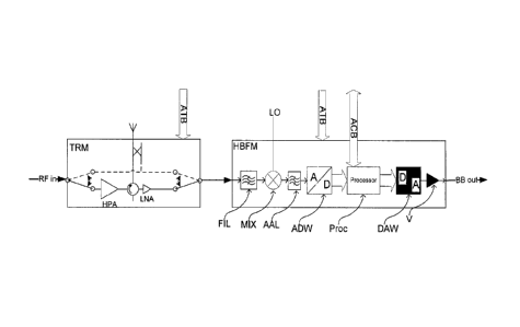
The more precise structure of the transmit/receive module and the hybrid beam
forming
module HBFM of the signal processing means according to the invention is shown
better in
Fig. 6. The hybrid beam forming module HBFM ¨ according to the digital signal
forming
unit according to the prior art ¨ comprises a filter FIL for signal filtering,
a mixer MIX for
down-mixing the analog receive signal into the baseband, an anti-alias filter
AAL, an analog-
to-digital converter ADW and a processor Proc for the application of beam
forming
algorithms for the current channel on the digital signal. In addition, the
hybrid beam forming
module HBFM comprises a digital-to-analog converter DAW arranged downstream of
the
processor Proc and an amplifier V. The signal BBout resulting herefrom is fed
to an analog
receive network, not shown in Fig. 6. In the embodiment according to the
invention of the
beam forming module a reading in of the output signal of the adjacent channel
via an HSSL
(high speed serial link) can be omitted.
A digitalization of the individual receive channels thus takes place in the
hybrid beam
forming module HBFM in order to be able to carry out the functions of beam
forming with
the necessary precision. The digitalization in the hybrid beam forming module
permits a
highly accurate synchronization of all of the channel signals before the
combination thereof
in the analog receive network.
The hybrid beam forming module can be implemented on a single chip in so-
called "mixed
signal" technology, which chip is inserted between a respective
transmit/receive module
TRM and the analog receive network not shown in Figs. 5 and 6. Particularly
preferably the
chip or the hybrid beam forming module is integrated into the transmit/receive
module.
The invention is thus based on the critical synchronization and channel
adjustment still taking
place in the digital range of the beam forming module. Only the simple
summation of the
data emitted per channel is carried out in an analog manner by a high
frequency signal
combination.
The analog output signal of each channel is located in or near to the baseband
and can
therefore be more easily controlled radiometrically than at carrier frequency.
With classic
{P42186 01469078.DOC}9
CA 02782440 2012-07-05
P42186.S01
SAR systems, the receive signals are combined and successfully calibrated at
carrier
frequency. A calibration of the receive signal network also takes place in the
SAR system
according to the invention, wherein the calibration signal is digitally
generated at the network
inputs.
A deterioration of the radar receive signal does not need to be accepted
because of the
insertion of the additional digital-to-analog converter DAW and of a further
analog-to-digital
converter provided according to the invention in thc central electronic system
shown in Fig.
2. An arbitrarily good quality of the analog signal can be achieved by means
of suitable
selection of the scanning rate and resoiution of the digital-to-analog
converter DAW. The
quantization noise thereby fed to the signal should be negligible compared to
the existing
inherent signal noise. The channel signal present before the digital-to-analog
conversion
basically has a high noise level (typically SNR < 16 db at highest dynamic
range) so that
digital-to-analog converters can already be used in the average power
spectrum.
The analog-to-digital conversion of the sum signal takes place in the central
electronic system
COMP, not shown in Figs. 4 through 9, apart from the antenna. It is sufficient
if the analog-
to-digital conversion of the sum signal takes place only once per panel.
Analog-to-digital
converters with high resolution (e.g., 12 bit) can bc used here. I he digital-
to-analog and
analog-to-digital conversion additionally inserted with respect to the
conventional beam
forming module is furthermore carried out with the hybrid beam forming module
on a signal
in or near to the baseband, whereby the demands on components and scanning are
substantially reduced compared to a signal in the carrier frequency band.
Iii an embodiment variant, not shown, several receive signals received by the
transmit/receivc
modules IRM can be connected to form one signal channel. This is in particular
expedient
when no hid demands are made on the antenna agility. In this manner the
antenna electronic
system can be further reduced in terms of its complexity. The availability of
the digital-to-
analog converter DAW in the beam forming module opens up further possibilities
if as
shown in Fig. 9 ¨ an additional line (feedback channel RC) is provided with an
upward mixer
MIX', amplifier V' and filter FIL'. The feedback channel RC is thereby coupled
to the input
of the transmit/receive module TRM. In this embodiment, the processor PROC can
generate a
digital chirp signal during the transmit pulse duration, which chirp signal is
modulated on the
carrier frequency and is conveyed as an input signal to the transmit/receive
module TRM. In
11)42186 01469078.DOCI10
CA 02782440 2012-07-05
P42186.S01
this casc the HU' network for the transmit signal can be omitted. This is
shown
diagrammatically in Fig. 8.
The advantages of this solution are a high radiometric accuracy, which can be
achieved with
the associated antenna. The hybrid beam forming module HBFM shown in Fig. 9
can be
calibrated particularly well if the closed calibration path CAL shown in Fig.
7 is adjusted. A
further advantage is the omission of a part of the central electronic system
for generating the
transmit signal and the transmit-side HF network. The locally generated
transmit signal does
not run through a long transmit network that has to be calibrated.
Furthermore, lower SRN
demands are made on the locally generated transmit signal than on a centrally
generated
transmit signal.
If a hybrid beam forming module HBFM embodied as in Fig. 9 is provided for
each
transmit/receive module TRM, all variable damping elements and phase control
elements can
be omitted.
The hybrid beam forming module provided according to the invention rcstricts
thc use of the
digital technology that is resource-intensive at high data rates to the
complex algorithmic
functions and leaves the simple summation of synchronous signals to the analog
range more
efficient here. This leads to a reduction in the complexity and quantity of
electronic systems
for the beam forming module on the antenna and thus to cost advantages. In
particular a
processor with reduced computing power compared to the prior art can be used.
Furthermore,
the HSSL chain members are omitted.
I he proposed architecture is inherently error redundant within the meaning of
a "graceful
degradation,- as with the transmit/receive modules TRM. Therefore no
redundancies are
necessary with the signal processing modules and data groups, which likewise
is beneficial in
terms of the quantity of electronic systems to be installed and consequently
to production
costs.
{P42186 01469078.D0011