Note: Descriptions are shown in the official language in which they were submitted.
CA 02782482 2012-05-31
1
Relief plug-in connector and multilayer circuit board
Prior Art
The invention relates to a multipolar relief plug-in connector for contacting
with a multilayer
circuit board, to a multilayer circuit board to be equipped with a multipolar
relief plug-in
connector, and to a combinatiOn of a multipolar relief plug-in connector and a
multilayer
circuit board provided to be equipped with the multipolar relief plug-in
connector.
Furthermore, the invention relates to a production method for the multilayer
circuit board.
A backplane implemented as a multilayer circuit board is known from patent
specification
US 5 543 586 A, which can be soldered to pins of contact elements. The contact
elements
can be assembled into groups of four. The individual contact elements of the
groups of four
can be soldered both to a single layer of the multilayer circuit board and
also to layers of the
multilayer circuit board located farther underneath.
A backplane which is implemented as a multilayer circuit board is described in
patent
specification US 7 278 855 B2. The circuit board can have multiple contact
area surfaces for
contact elements, for example, a first contact area surface in the middle of
the backplane and
a second contact area surface on the edge of the backplane.
Patent specification US 7 192 320 B2 and published application US 2009/0093173
Al
describe a multilayer circuit board, which can also have multiple contact area
surfaces, the
contact area surfaces being provided on individual layers of the multilayer
circuit board, so
that the contact area surfaces form a stepped structure. For example, in this
case a contact
area arranged in the middle area of the circuit board is provided with stepped
formations on
both sides and the contact area arranged on the edge is provided with a
stepped formation on
one side. The contact areas can be implemented with exclusively falling or
rising steps, but
also with both rising and also falling steps. Different contact areas can be
connected via
CA 02782482 2012-05-31
2
cables, which correspondingly have contact areas arranged in steps for
contacting the
stepped contact areas provided in the backplane. Furthermore, relief plug-in
connectors are
described, which are provided for contacting contact surfaces arranged on the
contact area
surfaces. The contacting sections of the contact elements of the relief plug-
in connector are
pressed onto the contact surfaces arranged on the contact area surfaces to
produce the
contact. The contacting sections of the contact elements can alternatively
also be soldered to
the contact surfaces arranged on the individual steps.
A plug connector is described in patent specification DE 699 15 882 T2, which
is suitable
for high-frequency data transmission. A contact element which conducts a
shielding or
ground potential is assigned to every contact element which conducts a signal.
The contact
elements are aligned in such a manner that an impedance adaptation is made
possible.
A plug connector is described in patent specification US 6 976 886 B2, in
which, through a
special arrangement and alignment of the contact elements conducting the
signal and the
contact elements conducting the shielding or ground potential, respectively,
to one another, a
high shielding effect of the lines conducting the signal to one another and of
the plug
connector as a whole is to be achieved. The known plug connector is especially
suitable for
high-frequency signals, the arrangement of the contact elements conducting the
signal and
the contact elements conducting the ground potential additionally being
specially predefined
to achieve a specific wave impedance.
A plug connector is described in published application DE 198 07 713 Al, which
contains a
large number of contact elements. The known plug connector is provided for
producing plug
connections between backplanes and plug-in cards, in the specific exemplary
embodiment,
plug connections being produced between backplanes and plug-in cards of so-
called
CompactPCI systems.
In the textbook by Meinke and Gundlach "Taschenbuch fur Hochfrequenztechnik
[Handbook for High-Frequency Technology], Springer Verlag 1956, pages 6-15, 48-
49, and
CA 02782482 2016-07-14
3
158-169, basic terms of electrical engineering such as capacitance,
inductance, and
wave impedance are explained.
The invention is based on the object of respectively specifying a multipolar
relief
plug-in connector for contacting with a multilayer circuit board, a multilayer
circuit
board to be equipped with a multipolar relief plug-in connector, a combination
of a
multipolar relief plug-in connector and a multilayer circuit board provided to
be
equipped with the multipolar relief plug-in connector, and a production method
for
the multilayer circuit board, which allow reliable contacting at low
manufacturing
costs.
The objects are respectively achieved by the features specified in the
independent
claims.
Summary of the Invention
According to the present invention there is provided a multipolar relief plug-
in
connector for contacting with a multilayer circuit board, which has a
plurality of
contact elements, whose contacting sections are arranged in height-offset
contact
area surfaces forming stepped arrangements, wherein the contact elements in
the
contacting section are implemented as press-in contacts to be pressed into
press-in
contact receptacles of the multilayer circuit board, wherein the press-in
contacts at
least approximately have equal lengths, wherein the press-in contacts are
arranged
adjacent to one another in a connecting line and form signal press-in contact
pairs,
and wherein at least one shielding press-in contact arranged adjacent is
assigned to
the press-in contact pairs.
According to the present invention there is also provided a multilayer circuit
board to
be equipped with a multipolar relief plug-in connector, which has multiple
height-
offset contact area surfaces forming stepped arrangements, wherein contact
CA 02782482 2016-07-14
3a
receptacles, which are implemented as press-in contact receptacles, are
arranged
in the contact area surfaces.
According to the present invention there is also provided a combination of at
least
one multipolar relief plug-in connector and a multilayer circuit board, the
relief plug-
in connector having a plurality of contact elements, whose contacting sections
are
arranged in height-offset contact area surfaces forming stepped arrangements,
and
the multilayer circuit board having multiple height-offset contact area
surfaces
forming stepped arrangements, wherein the contact elements of the relief plug-
in
connector are implemented in the contacting section as press-in contacts to be
pressed into press-in contact receptacles of the multilayer circuit board, and
contact
element receptacles, which are implemented as press-in contact receptacles,
are
arranged in the contact area surfaces of the multilayer circuit board.
Preferred embodiments are described hereunder.
The multipolar relief plug-in connector for contacting with a multilayer
circuit board
proceeds from a plurality of contact elements, which are arranged in height-
offset
contact area surfaces. The relief plug-in connector according to the invention
is
distinguished in that the contacting sections of the contact elements are
implemented as press-in contacts to be pressed into press-in contact
receptacles of
a multilayer circuit board.
The relief plug-in connector according to the invention can be contacted
particularly
simply and in particular cost-effectively with the multilayer circuit board
using the
measure provided according to the invention. Previously provided soldering and
the
thermal stress accompanying it of both the relief plug-in connectors and also
the
multilayer circuit boards are omitted completely.
The press-in contacts can be produced particularly simply by stamping, a
springy
element arising in the contacting section, which forms the press-in contact.
CA 02782482 2012-05-31
4
Advantageous embodiments and refinements of the relief plug-in connector
according to the
invention result from dependent claims.
An advantageous embodiment provides that the contacting sections of the
contact elements
are implemented as equally long. The uniform embodiment allows particularly
efficient
manufacturing of the press-in contacts.
Another embodiment provides that the press-in contacts are arranged adjacent
to one another
in an imaginary connecting line and preferably respectively form signal press-
in contact
pairs arranged adjacent. The signal press-in contact pairs are particularly
suitable for
conducting differential signals due to the resulting symmetrical structure.
A refinement of this embodiment provides that at least one shielding press-in
contact
arranged adjacent is assigned to the press-in contact pairs. The at least one
shielding press-in
contact is preferably arranged laterally offset in relation to the
respectively assigned signal
press-in contact pairs in such a manner that it does not lie on the signal
press-in contact pair
connecting line.
The structure thus resulting can be implemented having a predefined wave
impedance by
predefined geometric relationships and with incorporation of the provided
dielectric
material. A high signal integrity is achieved, whereby the relief plug-in
connector according
to the invention is suitable in particular for conducting high-frequency
signals up to well into
the gigahertz range.
The multilayer circuit board according to the invention to be equipped with a
multipolar
relief plug-in connector proceeds from the idea that the multilayer circuit
board has multiple
height-offset contact area surfaces. The multilayer circuit board according to
the invention is
distinguished in that contact receptacles, which are implemented as press-in
contact
receptacles, are respectively arranged in the contact area surfaces.
CA 02782482 2012-05-31
The multilayer circuit board according to the invention is especially embodied
to be suitable
for being equipped with the plug-in connector according to the invention.
Advantageous embodiments and refinements also result here from the dependent
claims.
One embodiment provides that electrically conductive bushes for electrical
contacting with
the press-in contacts of the relief plug-in connector are introduced into the
press-in contact
receptacles. The bushes are particularly mechanically robust and allow both
secure
mechanical and also electrical contacting.
One embodiment provides that at least some bushes extend over the entire
height of the
multilayer circuit board. The comparatively large electrically conductive
surface results in a
good shielding effect, because of which these bushes are provided in
particular for
contacting with the shielding press-in contacts of the relief plug-in
connector.
One embodiment provides that the links of the bushes are fixed at predefined
values. In this
case, the bushes are provided in particular for contacting with signal press-
in contact pairs,
the symmetrical line guiding being in the foreground. The short bushes
minimize the
undesired capacitances occurring between the press-in contact receptacles.
The combination according to the invention of at least one multipolar relief
plug-in
connector and one multilayer circuit board presumes that the relief plug-in
connector has a
plurality of contact elements, whose contacting sections are arranged in
height-offset contact
area surfaces, and the multilayer circuit board also has multiple height-
offset contact area
surfaces. The combination is distinguished in that the contact elements of the
relief plug-in
connector in the contacting section are implemented as press-in contact
elements to be
pressed into press-in contact receptacles of the multilayer circuit board, and
contact
receptacles, which are implemented as press-in contact receptacles, are
arranged in the
contact area surfaces of the multilayer circuit board.
CA 02782482 2012-05-31
6
The combination according to the invention unifies the above-described
advantages of the
individual components of the combination.
The method according to the invention, which is also provided, for producing a
multilayer
circuit board to be equipped with at least one relief plug-in connector, the
multilayer circuit
board having multiple height-offset contact area surfaces, provides that press-
in contact
receptacles are arranged in the contact area surfaces, which are produced by
means of bores,
electrically conductive bushes are introduced into the bores, the bushes are
drilled out from
the equipping side of the multilayer circuit board to the heights of the
respectively provided
contact area surfaces, and sO)sequently the contact area surfaces of the
multilayer circuit
board located at different heights are produced.
The production method according to the invention allows efficient
manufacturing of the
multilayer circuit board according to the invention.
One embodiment of the production method according to the invention provides
that at least
some bushes are additionally drilled out from the rear side of the multilayer
circuit board,
opposite to the equipping direction of the multilayer circuit board, so that
the bushes have a
predefined length which is less than the height of the respective contact area
surface of the
multilayer circuit board. This procedure is applied in particular in the case
of bushes which
are provided for contacting with the signal press-in contact pairs.
Further advantageous refinements and embodiments of the relief plug-in
connector
according to the invention, the multilayer circuit board according to the
invention, the
combination of relief plug-in connector and multilayer circuit board, and the
production
method according to the invention of the multilayer circuit board result from
the following
description.
Brief Description of the Figures
CA 02782482 2012-05-31
7
In the figures:
Figure 1 shows a view of relief plug-in connectors according to the
invention before
the contacting with multilayer circuit boards according to the invention,
Figure 2 shows a longitudinal section through a multilayer circuit
board according to
the invention, which is contacted with a relief plug-in connector according to
the invention embodied as a female connector,
Figure 3 shows a longitudinal section through a multilayer circuit
board according to
the invention, which is contacted with a relief plug-in connector according to
the invention embodied as a male header,
Figure 4 shows a detail view in the area of the contacting of a
multilayer circuit board
according to the invention in multiple sections, which is equipped with a
relief plug-in connector according to the invention,
Figure 5 shows a first step of a production method according to the
invention of a
multilayer circuit board according to the invention,
Figure 6 shows a second step of a production method according to the
invention of a
multilayer circuit board according to the invention,
Figure 7 shows a first embodiment of contact area surfaces of a
multilayer circuit
board according to the invention, and
Figure 8 shows a second embodiment of contact area surfaces of a multilayer
circuit
board according to the invention.
Description of Embodiments
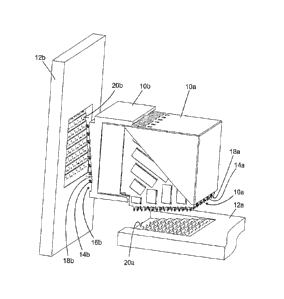
Figure 1 shows a view of relief plug-in connectors 10a, 10b according to the
invention
before the contacting with multilayer circuit boards 12a, 12b according to the
invention. In
this case, a relief plug-in connector 10a according to the invention is
implemented as a
female connector and a corresponding relief plug-in connector 10b is
implemented as a male
header, which are both shown in the plugged-in state. The multilayer circuit
board 12a is
CA 02782482 2012-05-31
8
implemented as a daughter card and the multilayer circuit board 12b is
implemented as a
backplane, for example.
The relief plug-in connectors 10a, 10b according to the invention each have a
plurality of
contact elements 14a, 14b, whose contacting sections 16a, 16b are arranged in
respectively
arranged height-offset contact area surfaces 18a, 18b.
The multilayer circuit boards 12a, 12b according to the invention each have
contact area
surfaces 20a, 20b corresponding to the contact area surfaces 18a, 18b of the
relief plug-in
connectors 10a, 10b.
The respectively arranged height-offset contact area surfaces 18a, 18b, 20a,
20b form
stepped anangements, which gives the visual impression of a relief, because of
which the
plug connectors 10a, 10b are designated as relief plug-in connectors 10a, 10b.
Figure 2 shows a longitudinal section through the multilayer circuit board
12a, 12b
according to the invention, which is contacted with the relief plug-in
connector 10a
according to the invention, embodied as a female connector, and Figure 3 shows
a
longitudinal section through the multilayer circuit board 12b according to the
invention,
which is contacted with the relief plug-in connecor 10b according to the
invention,
embodied as a male header. Both sections through the multilayer circuit board
12a, 12b
show that the contacting sections 16a, 16b of the relief plug-in connectors
10a, 10b are
implemented according to the invention as press-in contacts 22a, 22b.
The parts shown in Figures 2 and 3 which correspond to the parts shown in
Figure 1 each
bear the same reference numerals. This convention also applies for the
following figures.
The press-in contacts 22a, 22b are pressed into corresponding press-in contact
receptacles
24a, 24b in the multilayer circuit board 12a, 12b in the contacted state.
CA 02782482 2012-05-31
9
Figure 4 shows a greatly enlarged illustration of the press-in contacts 22,
Figure 4
illustrating the combination of the relief plug-in connector 10 according to
the invention
with the multilayer circuit board 12 according to the invention as an example.
The
differentiation between the reference sign supplements "a" and "b" is omitted.
The
description is to apply throughout, however, to both the plug-in connector 10a
embodied as a
female connector, whose components are to be designated with the reference
sign
supplement "a", and also for the plug-in connector 10b embodied as a male
header, whose
components are to be designated with the reference sign supplement "b". This
convention
also applies accordingly for the following figures and the further
description, respectively.
The press-in contacts 22 can be produced, for example, by stamping, a springy
element
resulting, which can be pressed into the press-in contact receptacle 24 of the
multilayer
circuit board 12.
Figure 4 shows an embodiment in which the contacting section 16 of the press-
in contacts 22
have equal lengths. Using this embodiment, the contact elements 14 having the
press-in
contacts 22 can be manufactured cost-effectively in the context of mass
production.
Figure 4 shows a further embodiment, according to which signal press-in
contact pairs 26 are
provided, which can be arranged adjacent with a preferably predefined spacing
from one
another. Furthermore, shielding press-in contacts 28 can be provided, which
are provided,
for example, for contacting electrically conductive shielding lamellae 30
provided in the
plug-in connector 10. Of course, individual signal press-in contacts can be
provided
additionally to or instead of signal press-in contact pairs 26.
The electrical contacting in the press-in contact receptacles 24 is produced,
for example, by
means of electrically conductive bushes 32, 34. An advantageous embodiment is
shown in
which the contact elements 14 conducting the signal, for example, the signal
press-in contact
pairs 26, can be assigned shorter bushes 34, and the shielding press-in
contacts 28 can be
assigned longer bushes 32. The bushes 32, 34 therefore have predefined lengths
36.
CA 02782482 2012-05-31
The signal press-in contact pairs 26 allow symmetrical line guiding not only
within the plug
connector 10, but rather in particular also in the contacting section 16 of
the press-in contacts
22, 26, 28 or in the press-in contact receptacles 24, respectively. Extremely
small runtime
differences between the signals may thus be implemented. Small runtime
differences are
particularly essential if the signal press-in contact pairs 26 conduct
differential signals, for
example, digital signals in the range up to 40 Gbit/s, which are still to be
transmitted error-
free with the most wide-open land pattern possible.
10 The specification of a determined differential wave impedance plays a
role here, for
example, 100 ohm, for a signal press-in contact pair 26, the wave impedance,
whose
definition can be inferred from the textbook by Meincke and Gundlach already
mentioned
above at the beginning, being substantially influenced through the geometric
embodiment of
the contact elements 14, i.e., their shape and spacing to one another, and by
the dielectric
material provided between the signal press-in contact pair 26. The shielding
press-in contact
28 is also significant, which ensures high signal integrity together with the
shielding
lamellae 30.
Geometric relationships with respect to signal press-in contact pairs 26 and
shielding press-
in contact 28 are illustrated in following Figure 5, on the basis of which the
first steps of the
production method according to the invention of the multilayer circuit board
12a, 12b are
also explained.
Figure 5 illustrates the arrangement of the signal press-in contact pairs 26
(not shown) on the
basis of the arrangement of the associated press-in contact receptacles 38.
One or preferably
multiple signal press-in contact pairs 26 are arranged adjacent to one another
on an
imaginary connecting line 40. A predefined spacing 42 is preferably
respectively provided
between individual signal press-in contacts of the signal press-in contact
pairs 26.
CA 02782482 2012-05-31
11
The shielding press-in contacts 28 (not shown) or the corresponding shielding
press-in
contact receptacles 44 are preferably located with an offset 46 adjacent to
the connec:ing line
40. Multiple shielding press-in contact receptacles 44 are preferably
provided, which are
then also preferably arranged on an imaginary connecting line.
The production method proceeds from a multilayer circuit board 12 having a
specific height
48. The press-in contact receptacles 24, 38, 44 are drilled by means of a
drill 50 in the
equipping direction 52 through the entire height 48 of the multilayer circuit
board 12.
Subsequently, the bushes 32, 34 are produced in the press-in contact
receptacles 24, 38, 44,
preferably by a galvanic deposition method. The bushes 32, 34 are then
preferably drilled
out frorn the equipping side at least to a height 54, which can at least
approximately
correspond later to the height 54 of the affected contact area surface 20.
In the subsequent processing step, which is shown in Figure 6, at least some
bushes 34 can
be drilled out opposite to the equipping direction 52 up to the predefined
length 36 from the
rear side 56 of the multilayer circuit board 12. The signal-conducting press-
in contacts 22,
26 are preferably pressed later into these bushes 34. The undesired
capacitances occurring
between the press-in contact receptacles 38 are reduced by the shortening of
the bushes 34.
Some bushes 32 are not drilled out from the rear side. The shielding press-in
contacts 28 are
preferably pressed later into these bushes 32, whose height 58 later at least
approximately
corresponds to the height of the contact area surface 20. The larger metallic
surface of the
un-shortened bushes 32 supports the shielding effect.
In the last processing step, the contact area surfaces 20 are produced in the
various heights
58 of the multilayer circuit board 12, preferably by milling. Figures 7 and 8
show various
possibilities for implementing the contact area surfaces 20 for this
production step.
According to Figure 7, a continuously rising or continuously falling staircase
is provided.
Different heights 60, 62 are also indicated. Furthermore, a short bush 32 and
a long bush 34
CA 02782482 2012-05-31
12
are shown in the sectional view. A rising and also falling staircase is shown
according to
Figure 3.