Note: Descriptions are shown in the official language in which they were submitted.
CA 02782486 2012-06-28
1
TITLE OF THE INVENTION
MATCHED HIGH-SPEED INTERCONNECTOR ASSEMBLY
FIELD OF THE INVENTION
[0002] The present invention relates to a matched high-speed
interconnector assembly. In particular, the present invention relates to a
matched plug and receptacle pair comprising a compensation which allows
either the plug or the receptacle to form part of a legacy network.
BACKGROUND TO THE INVENTION
[0003] Many prior art plug and connector systems based on the
ubiquitous RJ-45 standard suffer from the limitation that in order to
correctly
mate plug and connector, the pair comprised of conductors 3 and 6 is
separated by the pair comprised of conductors 4 and 5. This means that, in
order to terminate a cable, the pairs are inevitably crossed thereby
introducing small areas of reactive coupling that, at higher frequencies,
unbalance the resultant connection. As a result, such prior art plug and
connector systems are typically unsuitable for use at higher data rates.
[0004] Prior art systems have addressed the above drawback by
reorganizing the order of the connectors such that such crossing can be
avoided. However, the resultant plugs and connectors of such systems are
not backwardly compatible, and an adaptor or the like must be used to
achieve compatibility with legacy plugs and connectors.
SUMMARY OF THE INVENTION
CA 02782486 2012-06-28
2
[0005] In order to address the above and other drawbacks, there is
provided a compensating interconnection assembly for interconnecting a
first cable comprised of four pairs of conductors with a second like cable of
four pairs of conductors. The assembly comprises a plug comprising a plug
body for terminating the first cable at a rear thereof wherein each conductor
of the pairs of conductors of the first cable is interconnected with a
respective one of eight evenly spaced terminal contacts exposed along a
front of the plug body and via a first compensating network, a receptacle
configured for receiving the plug body front and comprising eight evenly
spaced conductive tines therein, wherein one of each of the tines
interconnects with a respective one of the eight evenly spaced terminal
contacts when the plug is mated with the receptacle, one of each of the
tines connected with a respective conductor of the pairs of conductors of
the second cable via a second compensation network. Each of the first
compensation network and the second compensation network are
complementary and each contributes to provide an overall compensation
better than a compensation provided separately by said first compensation
network and said second compensation network.
[0006] There is further provided a cable assembly for use in a
telecommunications system comprising a cable comprising four pairs of
conductors, and a RJ-45 style plug comprising a plug body for terminating
the cable at a rear end thereof, eight evenly spaced terminal contacts
exposed along a front of the plug body and a flexible printed circuit board
comprising a plurality of pairs of traces interconnecting each conductor of
the pairs of conductors with respective ones of the terminal contacts and a
compensating network comprising a plurality of capacitive reactances. A
first pair of the pairs is attached to a first pair of the traces towards a
first
end of the flexible printed circuit board and the remaining pairs of
conductors are attached to their respective pairs of traces towards a
CA 02782486 2012-06-28
3
second end of the flexible printed circuit board, wherein the flexible printed
circuit board comprises a fold towards a middle thereof such that the first
end and the second end lie opposite one another and further wherein the
traces contact their respective terminal contacts adjacent the fold.
BRIEF DESCRIPTION OF THE DRAWINGS
[0007] Figure 1 is right front perspective view of a high speed
interconnection assembly in accordance with an illustrative embodiment of
the present invention;
[0008] Figure 2 provides a plurality of different views of a cable
assembly and plug in accordance with an illustrative embodiment of the
present invention;
[0009] Figures 3A and 3B provide plan views of a complementary
flexible PCB pairs and their respective artwork in accordance with an
illustrative embodiment of the present invention;
[0010] Figure 4 provides a cut-away side plan view of a plug and
receptacle assembly in accordance with an illustrative embodiment of the
present invention;
[0011] Figures 5A and 5B provide schematic diagrams of a pair of
complementary compensation networks in accordance with an illustrative
embodiment of the present invention; and
[0012] Figure 5C provides a detailed perspective view of an
illustrative interconnection between a plug and receptacle of the present
invention.
CA 02782486 2012-06-28
4
DETAILED DESCRIPTION OF THE ILLUSTRATIVE EMBODIMENTS
[0013] Referring now to Figure 1, a matched high speed
interconnection assembly, generally referred to using the reference numeral
10, will now be described. The system 10 comprises a cable 12 terminated
by a plug 14 which is adapted for insertion into a connector receptacle 16
mounted in a patch panel 18 or the like which typical comprises a plurality
of such connector receptacles.
[0014] Referring to Figure 2, the cable 12 comprises a plurality of
pairs of conductors 20 which are interconnected with a respective one of a
plurality of terminal contacts 22 positioned toward a front end 24 of the plug
14. Illustratively, a flexible Printed Circuit Board (PCB) 26 comprising a
plurality of traces 28 etched or otherwise formed on a dielectric substrate
30 is used to interconnect each conductor as in 20 with its respective
terminal contact 22. The flexible PCB 26 is folded over on itself and
illustratively supported by a rigid support 32. Alternatively, and as will be
discussed in more detail below, the flexible PCB 26 can be replaced by a
multi-layer PCB with provision of the appropriate VIAs and the like (not
shown). The plug 14 also includes a locking tab 34 for releasably securing
the plug 14 in the connector receptacle 16.
[0015] Referring now to Figure 3A, as discussed above the flexible
PCB 26 comprises a plurality of traces 28 etched or otherwise formed on
both surfaces of a dielectric substrate 30, the compensation layer artwork
on a first surface and the contact layer artwork on a second surface. Traces
as in 28 on a first side of the board are interconnected with traces as in 28
on an opposite side of the dielectric substrate by a Vertical Interception
Access (VIA) as in 34, which provides a conductive path through the
dielectric substrate 30. A contact pad 36 is provided at an end of each
CA 02782486 2012-06-28
conductive path and is suitable for attachment to a respective conductor as
in 20, typically by means of a piercing contact of the like (not shown). The
terminal contacts as in 22 are positioned such that when the flexible PCB
26 is folded along a line within a folding region 38 and inserted into the
plug
5 14, the terminal contacts 22 are exposed toward a front end 24 of the
plug
14, and as illustrated in Figure 2. A support (not shown) is typically
provided
around which the flexible PCB 26 is folded in order to ensure that when
folded, the opposed surfaces of the flexible PCB 26 are maintained
sufficiently apart. Additionally, as will be discussed in more detail below,
additional conductive traces as in 28 act as conductive plates and the
dielectric substrate 30 as dielectric for a plurality of capacitive elements
in a
compensation network.
[0016] Still referring to Figure 3A, one advantage of the above
configuration is that inductive coupling is largely removed leaving a
compensating structure which is comprised mainly of capacitive reactances
which provides for simplified and improved compensating at higher
frequencies. Additionally, as will be discussed in more detail below,
compensating capacitances are introduced proximate to the point where
the parasitic coupling which gives rise to cross-talk is introduced.
[0017] Referring back to Figure 1, it is foreseen that a plug 14
comprising the flexible PCB 26 of Figure 3A is configured to interconnect
with a complementary receptacle 16 comprising a second flexible PCB 40
of Figure 3B. Indeed, as will be discussed below, in order to achieve the
preferred compensation, the plug 14 and receptacle 16 illustratively each
provide only a portion of the components necessary to achieve the high
speed connector of the present invention. The components of the plug 14
and receptacle 16 therefore work together to achieve the high speed
connector of the present invention.
CA 02782486 2012-06-28
6
[0018] Referring now to Figure 3B, the second flexible PCB 40 is
similarly comprised of a plurality of traces as in 42 etched or otherwise
formed on the surface of a flexible dielectric substrate 44, the compensation
layer artwork on a first surface and the contact layer artwork on a second
surface. The traces 42 interconnect a plurality of contact pads as in 46 with
their respective terminal contacts as in 48. Similar to the plug 14,
additional
conductive traces as in 42 act as conductive plates and the dielectric
substrate 44 as dielectric for a plurality of reactive elements which serve as
capacitive elements in a compensation network. In an alternative
embodiment, slots as in 50 can be punched or otherwise formed in the
dielectric substrate 44 in order to allow the terminal contacts as in 48 to
flex
lightly when, as will be seen below, the come into contact with the terminal
contacts 22 of the plug 14.
[0019] Referring now to Figure 4 in addition to Figure 3B, given the
complementary nature of the first flexible PCB 26 and the second flexible
PCB 40 and in order to simplify the connection between the plug 14 and
receptacle 16, the second flexible PCB 40 is also used to terminate a
second cable 52 using a second plug 54 (designated B) in a manner
essentially the same as that described hereinabove. Indeed, referring back
to Figure 3B, the terminal contacts as in 48 are positioned such that when
the flexible PCB 40 is folded along a line within a folding region 56, the
terminal contacts 48 are exposed toward a front end 58 of the second plug
52. In order to interconnect the terminal contacts 22 of the first plug 14
with
their respective terminal contacts 48 of the second plug 52, a series of
conductive interconnecting bridging contacts, or tines 58 are provided
within the receptacle 16. As will now be apparent to a person of ordinary
skill in the art, insertion of the first plug 14 into the first complementary
socket 60 formed in the receptacle 16 and insertion of the second plug 52
CA 02782486 2012-06-28
7
into the second complementary socket 62 formed in the receptacle 16, the
terminal contacts 22 of the first plug 14 are interconnected with their
respective terminal contacts 48 of the second plug 52 through provision of
the conductive interconnecting bridging contacts 58.
[0020] Referring back to Figure 3B, alternatively, and as discussed
briefly above, the second flexible PCB 40 can be provided with a series
slots as in 50 between each of the terminal contacts as in 48 and positioned
within the connector receptacle (reference 16 on Figure 1). Provision of the
slots as in 50 allows the terminal contacts as in 48 to function as tines. As
will now be apparent to a person of ordinary skill in the art, on insertion of
the plug 14 into the receptacle 16, the plug terminal contacts 22 come into
contact with a respective one of the receptacle terminal contacts as in 48,
thereby completing the connection.
[0021] Referring now to Figures 5A and 5B in addition to Figures 3A
and 3B, the terminal contacts 22, 48 introduce small wire-to-wire parasitic
capacitances Cp (reference 66) which at high transmission frequencies give
rise to cross talk. In order to compensate for these parasitic capacitances,
and as briefly discussed above, particular ones of the traces 28, 42 also
serve to form capacitive elements as in 68 which are introduced into the
transmission path in a controlled manner and together form a compensating
network. Of note is that only those parasitic capacitances between adjacent
terminal contacts as in 22, 48, given their proximity, need to be taken into
account as parasitic coupling between terminal contacts which are not
adjacent is negligible.
[0022] One major advantage of the present configuration is that the
compensating capacitances are introduced at substantially the same
location as where the parasitic capacitances occur. Indeed, referring to
CA 02782486 2012-06-28
8
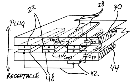
Figure 5C when the plug is inserted into the receptacle socket the plug
terminal contacts 22 come into contact with their respective receptacle
terminal contacts 48 thereby providing a transmission path between the
respective conductors of the cables attached to the plug and the receptacle.
Between contacts terminating conductors 2 and 3, for example, parasitic
coupling due to parasitic capacitance Cp23 occurs which at higher
transmission speeds introduces cross talk into the transmission. In order to
compensate for the parasitic coupling, capacitances C13 and C23 are
introduced through positioning of traces 28, 42 opposite their respective
terminal contacts 22, 48 which both act as electrodes of their respective
capacitance C13, C23 formed of the respective dielectric substrate 30, 44.
The traces 28, 42 additionally provide the respective connections to the
respective terminal contacts as required and according to the artwork as
described hereinabove in Figures 3A and 3B.
[0023] Still referring to Figure 5C, introduction of the
compensating
capacitances at substantially the same location as where the parasitic
capacitances occur limits the amount of phase shift and the like which
might occur and perturb the compensation. In particular, a maximum
distance equivalent to A/12 at the greatest operating frequency between
contact coupling and compensation ensures that the effects of inductive
coupling are negligible. For example, at 500MHz A=40cm, and therefore
A/12=-,33.3mm. Similarly, at 2GHz A~10cm and A/12Az8.33mm.
[0024] Referring back to Figures 5A and 5B, in a first illustrative
embodiment the capacitive elements Cxy as in 68 can be chosen arbitrarily
and such that they are much larger than the parasitic capacitances Cp 66,
i.e. Cxy >> Cp. Additionally, the individual capacitive elements 66 are
illustratively selected to fulfil the following:
CA 02782486 2012-06-28
9
C13 C23
C34 = C35
C16 C26
C67 C68
C56 = C46
C38 C37
[0025] Still referring to Figure 5A and Figure 5B, as will now be
apparent to a person of ordinary skill in the art, given selection of the
capacitive elements 68 according to the above, respective compensating
network portions of the plug (Figure 5A) and the receptacle (Figure 5B) are
complementary and that, when assembled together, provide an overall
compensation better, or improved, over the compensation provide by the
plug and jack/receptacle alone.
[0026] Referring back to Figure 1 in addition to Figure 5A and Figure
5B, an additional advantage of the present invention is that the values of
the compensating capacitances Cxy (reference 68) of both the plug 14 and
receptacle 16 can be chosen such that the plug 14 and receptacle 16 are
compatible with legacy connectors (not shown) conforming to the legacy
TIA Cat5 and Cat6 standards. Indeed, the compensation of the plug 14 is
such that when the cable 12 and plug 14 of the present invention is used in
a legacy system, the compensation insures that the assembly meets the
performance specification of the legacy standard. The same applies to the
receptacle 16 when used as a component in a legacy system.
[0027] Still referring to Figures 5A and 5B, in order to determine
the
values of the compensating capacitances Cy, the legacy TIA standards
provide that, in a mated connection, Near End Cross Talk (NEXT) must fall
within the following ranges for the respective indicated conductor pairs at
CA 02782486 2012-06-28
100MHz:
= -38.1 dB > NEXT(36-45) > -39.5 dB with a phase of -90
= -46.5 dB > NEXT(12-36) > -49.5 dB with a phase of -90
5 = -46.5 dB > NEXT(36-78) > -49.5 dB with a phase of -90
= -57 dB > NEXT(12-45) > -70 dB with a phase of +90
= -57 dB > NEXT(45-78) > -70 dB with a phase of +90
= -66 dB > NEXT(12-78) > -00 any phase
10 [0028] Therefore, by designing the plug and the receptacle such
that
they individually meet the above standard, correct operation in combination
with (an uncompensated) legacy equipment can be assured.
[0029] Capacitance is proportional to (NEXT+FEXT)/2 (FEXT = Far
End Cross Talk) and inductance is proportional to (NEXT-FEXT)/2. In the
case, as in the present, where inductance is near to zero, NEXT FEXT.
[0030] Assuming that that the parasitic capacitances Cp are less than
0.05pF (Cp < 0.05 pF), then by selecting the compensating capacitances
Cy according to the following table, a compensation scheme can be
arrived that improves overall compensation at high speeds when the plug is
used in combination with the receptacle of the present invention while at the
same time meeting the legacy standards when the plug of the present
invention is used with a legacy receptacle or alternatively a legacy plug is
used with the receptacle of the present invention:
Plug Receptacle
C34 C56 0.5 pF C35 C467,-, 0.5 pF
C23 C16 0.2 pF C13 :=C26 0.2 pF
CA 02782486 2012-06-28
11
C38 .----. C67 ....--= 0.2 pF C37 2-=== C68 ;--- 0.2 pF
[0031] As both the plug and receptacle give rise to NEXT between
pairs 12-36 of less than -39dB at 100MHz, the mated connection between
plug and receptacle is typically somewhat better than this. When mated,
assuming that less than about 4% difference (error) between the plug and
receptacle of the present invention will give rise to less than about -54dB
cross talk at 100MHz. Between pairs 12-36, NEXT varies more or less
linearly in the range from 100MHz to 2GHz, according to the equation:
(1) NEXT = -54dB + 201og10(f/100MHz)
[0032] Given the above equation, it is expected that at 500MHhz, the
mated connection will give rise to be about -40dB of cross talk and at
2GHz, about -28dB.
[0033] Although the present invention has been described
hereinabove by way of specific embodiments thereof, it can be modified,
without departing from the spirit and nature of the subject invention as
defined in the appended claims.