Note: Descriptions are shown in the official language in which they were submitted.
CA 2782710 2017-04-19
WO 2011/067297 PCT/EP2010/068658
MICROFABRICATED NEUROSTIIVIULATION
DEVICE AND METHODS OF MAKING AND USING THE SAME
CROSS REFERENCE TO RELATED APPLICATION
10011 The present application claims benefit of U.S. Provisional Application
Serial Number
61/265,725 filed December 1, 2009 .
FIELD
100021 The present disclosure relates generally to the field of interacting
with biological tissue
through the use of electrical probes, and more particularly to interacting
with a neurological target
through the use of inieroelectmie probes.
BACKGROUND
10003] Neurostimulation is a category of medical devices that are used to
transfer electric
charge or electrical fields to tissue and result in a physiological change
which benefits the patient,
or performs a physiological measurement. Neurostimulation is used today in the
cochlea, the
retina, the peripheral nerve system, the spine, the brain and other parts of
the body.
100041 In a particular application of Neuromodulation, conductive electrodes
are placed in
contact with certain cortical brain structures in order to treat certain
neurological conditions. In
the case of stimulating the cortical surface, for example, as described in US.
Pat. App.
2008/0045775, the stimulation may relieve the symptoms of Parkinson's Disease,
other
movement disorders, or psychiatric disorders. In the case of stimulating an
associated region of
the cortical surface, for example, as described in US. Pat. 7,774,068, the
stimulation can treat the
symptoms of movement disorders including restless leg syndrome. In the case of
stimulating the
temporal love of the cortex, for example, as described in US. Pat. App.
2007/0055320 or
[Theodore, W.H., Fisher, R.S., "Brain stimulation for epilepsy", Lancet
Neurology, 3 (2), pp.
111-118, (2004).1, the stimulation can treat the symptoms of temporal lobe
epilepsy.
- 1 -
CA 02782710 2012-06-01
WO 2011/067297 PCT/EP2010/068658
100051 In the case where a cortical electrode array is used for recording and
stimulation in long
term therapy, an implantable pulse generator supplies the electrical signal to
the electrode lead in
contact with the brain structure. Additionally, the implantable pulse
generator can record neural
activity and electromagnetically transmit information outside the body. All
components are
placed surgically.
100061 In the case where a cortical electrode array is used for recording and
stimulation as a
diagnostic tool, it may be placed temporarily on the cortex, for example for a
few weeks, and then
removed when no longer required. The information can be captured using
wearable, or
implantable, or semi-implantable, hardware.
100071 In most prior art the electrode placed in contact with the cortex brain
tissue has been
metallic, disc like, and relatively large in size (e.g., 3 mm in diameter). In
many cases, the
electrodes are as large as the brain structures themselves. The large size of
electrodes prevents
specific and precise stimulation and recording of small brain targets which
may be responsible for
disease. The resulting large electric fields and associated current paths
stimulate other structures
of the cortex, and do not concentrate on the intended target. Furthermore,
these large electrodes
cannot be used to identify the targets of the brain by neural-recording
because the area they cover
is very large.
100081 Additionally, in most prior art, cortical electrodes are placed on the
surface of dura mater
which is an electrically insulating biomaterial. Placing electrodes on the
dura mater, so called
epidural electrode placement, prevents efficient charge transfer to and from
the brain region,
rendering stimulation and recording less efficacious. For example, electric
fields and associated
current paths established by an epidural electrode will not concentrate
electrical stimulation on
the intended target. This prevents the effective delivery of potentially
therapeutic or diagnostic
neural stimulation. Additionally, for example, neural signals that epidural
electrodes are trying to
capture will be very weak on the dural surface, and therefore signal-to-noise
ratio will be very
low. This prevents the reliable recording of diagnostically or therapeutically
useful neural
activity.
100091 Current techniques that determine placement of such relatively large
electrodes are
accomplished by first performing a craniotomy that can vary in size but is
usually at least 10 mm
in diameter and be as large as several centimeters. An electrode array is then
placed upon the
- 2 -
CA 02782710 2012-06-01
WO 2011/067297 PCT/EP2010/068658
surface of the cortex. Some surgeons may create a flap of the dura mater and
place the electrode
array directly on the cortical surface. Recordings of neural activity can be
made using the
electrode array, from several electrode contacts. This process is complex,
requiring a highly
skilled surgeon to place the electrode array, and usually a highly skilled
neurophysiologist to
interpret the neural recording data. The large craniotomies that have to be
performed put the
patient at risk of infection and serious collateral injury.
100101 Attempts have been made at developing microfabricated devices
specifically designed to
incorporate an array of microelectrodes which can stimulate small volumes of
tissue on the cortex
of the brain. Attempts have also been made to develop sub-dural penetrating
microelectrodes for
use on the cortex of the brain, for example, as described in U.S. Pat.
5,215,088, "Three-
Dimensional Electrode Device" by Nonnann et al. Additionally, descriptions
have been made in
[Richard et al., "A neural interface for a cortical vision prosthesis", Vision
Research, 39, pp.
2577-2587, (1999)]. The prior devices however have not been able to easily
translate to clinical
use even though they have been available for more than a decade. This may be a
result of the
1 5 materials that are required to construct the device, because Silicon is
a brittle material which may
easily break during implantation or removal. Additionally, the reason for the
lack of success may
be because their functions do not provide enough additional information to the
surgical team,
because they only provide one electrode per penetrating shaft.
[0011] An important requirement for a successful outcome of cortical
stimulation therapy, is the
accurate placement of the stimulation and recording electrodes within the
stimulation target area.
Mislocation may result in unwanted side-effects, including sensory motor
deficits. Additionally,
a mislocated recording electrode will yield little or no relevant
physiological data to the surgical
team. Prior art procedures approximately localize the target by pre-surgical
imaging and
planning, for example through Trans-Cranial Magnetic Stimulation as described
in [Komssi et al.,
"The effect of stimulus intensity on brain responses evoked by transcranial
magnetic
stimulation", Human Brain Mapping, 21(3), pp. 154-164, (2004)] to identify a
region of
therapeutic interest. The targets themselves may be only a few mm or less, and
not be detectable
through standard imaging techniques alone. Therefore exploratory surgical
procedures involving
acute stimulation, many times with the patient awake during the procedure, are
necessary. Once
- 3 -
CA 02782710 2012-06-01
WO 2011/067297 PCT/EP2010/068658
the precise target area is located, the acute or chronic recording and
stimulation electrodes can be
implanted at the precise location.
100121 Disadvantages of the current technology include extension of operation
time by several
hours, which can be an increased burden for the patient, who may be awake
during such
procedures, and extended cost associated with lengthier procedures which are a
heavy financial
burden on healthcare providers. Increased risk of surgical complications from
bleeding or tissue
damage caused by large craniotomies or repeatedly placed electrode arrays are
a major risk of
infection for the patient. Additionally, the possibility that chronic
electrode arrays are not
precisely located at identified target for any number of reasons, including
further brain movement
require that patients return to surgery.
SUMMARY
100131 For efficient stimulation of cortical brain structures, an array of
subdural penetrating
microelectrodes are required. After placement of the microelectrode array, the
surgeon should be
able to identify the area of the brain that requires stimulation by recording
from the
1 5 microelectrodes. Subsequently the surgeon should stimulate the
identified structure.
100141 For more efficient diagnostic and therapeutic use in cortical brain
structures, subdural
penetrating microelectrodes that create a three-dimensional volume of
stimulation and recording
functionality are described.
100151 The disclosure describes a system which places many microelectrode
structures on the
cortex of the brain, and allows the surgeon to apply a signal to each
microelectrode separately, in
parallel, or between at least two microelectrodes. Furthermore, using
electronics to record neural
activity from the system, the surgeon can develop a localized map of neural
activity in the cortical
region in which the electrode is implanted.
100161 In one aspect, the disclosure relates to an implantable neurological
probe. The
neurological probe includes at least one protrusion on which at least one
microelectrode elements
are disposed on the surface of the protrusion. The microelectrode elements can
perform neural
stimulation or neural recording. The neurological probe preferably has several
protrusions, and
the protrusions preferably have several microelectrodes elements, or an array
of microelectrode
elements. Attached to the neurological probe, either on its surface, or
connected through a
- 4 -
CA 02782710 2012-06-01
WO 2011/067297 PCT/EP2010/068658
tethered ensemble of wires, is the control circuitry. The control circuitry is
itself encapsulated in
a wearable or implantable enclosure. The neurological probe includes at least
one electrical
connection, or electromagnetic link, to the control circuitry. The control
circuitry sends
stimulation signals to the neurological probe. The control circuitry can also
capture
neurophysiological signals from the neurological probe. The control circuitry
may connect
telemetrically to yet another external controller, which can be used to
transmit signals to and from
the neurological probe, via the attached control circuitry.
[0017] In another aspect, the disclosure relates to a process for stimulating
a neurological target.
The process includes implanting a neurological probe at or near the target
site on the cortex. The
.. neurological probe itself comprises a supportive backing layer, at least
one protrusion from the
supportive backing layer, and at least one microelectrode element on each
protrusion.
Additionally, each of the at least one microelectrode elements are in
electrical communication
with either a proximal electrical contact, or in electrical communication with
the control circuitry.
The proximal electrical contact may be connected to a neurological stimulation
source supplying
1 5 an electrical signal. Alternatively, the control circuitry may be
supplying the electrical signal to
the microelectrode element. The supplied signal is applied to one or more of
the microelectrode
elements. The one or more energized microelectrode elements produce an
electric field adapted
to stimulate the neurological target site.
[0018] In yet another aspect, the disclosure relates to a process for
recording from a
.. neurological target. The process includes implanting a neurological probe
at or near the target
site on the cortex. The neurological probe itself comprises a supportive
backing layer, at least
one protrusion from the supportive backing layer, and at least one
microelectrode element on
each protrusion. Additionally, each of the at least one microelectrode
elements are in electrical
communication with either a proximal electrical contact, or in electrical
communication with the
control circuitry. The proximal electrical contact may be connected to a
neurological recording
source, such as an amplifier acquisition system. Alternatively, the control
circuitry may be
acquiring and recording the neurophysiological signal from the microelectrode
element. The
acquired signal may be transmitted from the control circuitry to the external
controller. The one
or more recorded microelectrode elements produce data on the
electrophysiological activity of the
neurological target site.
- 5 -
CA 02782710 2012-06-01
WO 2011/067297 PCT/EP2010/068658
100191 In another aspect, the disclosure relates to an implantable device
comprising several
neurological probes, where each neurological probes includes a supportive
backing layer, at least
one protrusion extending away from a surface of the supportive backing layer
and at least one
microelectrode element arranged along the at least one protrusion. The
neurological probes may
be connected to each other by tethered wires. Alternatively the neurological
probes may be in
telemetric communication.
100201 In another aspect, the disclosure relates to an implantable
neurological probe which
includes a supportive backing layer, at least one protrusion extending away
from a surface of the
supportive backing layer and at least one microelectrode element arranged
along the at least one
protrusion.
100211 In another aspect, the disclosure relates to a process for stimulating
a neurological target
by implanting a neurological probe within a vicinity of a cortical target
site. The neurological
probe includes a supportive backing layer, at least one protrusion extending
away from a surface
of the supportive backing layer. At least one microelectrode element is
arranged along the at
least one protrusion. The at least one microelectrode element is energized by
a supplied electrical
signal, wherein the at least one microelectrode element produces an electric
field adapted to
stimulate the neurological target site.
100221 In another aspect, the disclosure relates to an implantable
neurological surface probe
includes a supportive backing layer and a number of protrusions. Each
protrusion is attached at
one end to the supportive backing layer and extends away from a surface of the
supportive
backing layer. The probe also includes a microelectrode film disposed along at
least a portion of
the supportive backing layer. A number of microelectrode elements are disposed
on the
microelectrode film and arranged along each of the number of protrusions. Each
microelectrode
element is disposed at a respective depth measured from the surface of the
supportive backing
layer.
100231 In yet another aspect, the disclosure relates to a process of making an
implantable
neurological surface probe includes shaping a supportive backing layer and
defining within the
supportive backing layer a number of rigid backing members. Each of the rigid
backing members
has a tip at one end and is attached to the supportive backing layer at
another end. Each rigid
backing member is bent at its attached end away from a surface of the
supportive backing layer,
- 6 -
CA 02782710 2012-06-01
WO 2011/067297 PCT/EP2010/068658
forming a number of protrusions. A number of microelectrode elements are
formed on a
microelectrode film, and the microelectrode film is fastened along at least a
portion of the surface
the supportive backing layer. The film is fastened such that respective
subsets of the plurality of
microelectrode elements are arranged along each of the plurality of
protrusions. When so
arranged, each microelectrode element of each respective subset is disposed at
a respective depth
measured from the surface of the supportive backing layer.
BRIEF DESCRIPTION OF THE DRAWINGS
[0024] The foregoing and other objects, features and advantages of the
disclosure will be
apparent from the following more particular description of preferred
embodiments of the
disclosure, as illustrated in the accompanying drawings in which like
reference characters refer to
the same parts throughout the different views. The drawings are not
necessarily to scale,
emphasis instead being placed upon illustrating the principles of the
disclosure.
[0025] FIG. 1 is a perspective view of one embodiment of a cortical
neuromodulation device.
[0026] FIG. 2 is a perspective view of a portion of a human anatomy
illustrating an exemplary
cortical neuromodulation device implanted therein.
[0027] FIG. 3 is a cross-sectional view of a portion of a human cortex anatomy
illustrating an
exemplary neurological surface probe positioned on the surface of the brian.
[0028] FIG. 4 is a schematic view of the components that are incorporated in
the cortical
neuromodulation device.
[0029] FIG. 5A is a top view of the cortical neuromodulation device in FIG. 1.
[0030] FIG. 5B is detailed view of the control module of the cortical
neuromodulation device in
FIG. 1.
[0031] FIG. 6A is a detailed view of the neurological surface probe in FIG. 1.
[0032] FIG. 6B is an additional detailed view of the neurological surface
probe in FIG. 1.
100331 FIG. 6C is a perspective view of the neurological surface probe in FIG.
1 where currents
have been applied to the microelectrodes.
- 7 -
CA 02782710 2012-06-01
WO 2011/067297
PCT/EP2010/068658
100341 FIG. 6D is an additional perspective view of the neurological surface
probe in FIG. 1
where currents have been applied to the microelectrodes demonstrating electric
field isosurfaces.
[0035] FIG. 7A is a front view of the neurological surface probe in FIG. 1.
100361 FIG. 7B is a side view of the neurological surface probe in FIG. 1.
[0037] FIG. 7C is a top view of the neurological surface probe in FIG. 1.
[0038] FIG. 8A is a perspective view of a protrusion from the supportive
backing layer of the
neurological surface probe in FIG. 1.
[0039] FIG. 8B is an additional perspective view of a protrusion from the
supportive backing
layer of the neurological surface probe in FIG. 1.
[0040] FIG. 9 is a top view of the supportive backing layer and microelectrode
film that are
incorporated in a neurological surface probe before they have been attached.
[0041] FIG. 10 is a top view of the supportive backing layer and
microelectrode film that are
incorporated in a neurological surface probe after they have been bonded.
[0042] FIG. 11A is a perspective view of a cross section of human anatomy
demonstrating the
placement of the cortical neuromodulation device of FIG. 1.
[0043] FIG. 11B is an additional perspective view of a cross section of human
anatomy
demonstrating the placement of the cortical neuromodulation device of FIG. 1.
[0044] FIG. 11C is an additional planar view of a cross section of human
anatomy
demonstrating the placement of the cortical neuromodulation device of FIG. 1.
.. 100451 FIG. 12 is a perspective view of an alternative embodiment of a
cortical
neuromodulation device.
[0046] FIG. 13 is an additional perspective view of the alternative embodiment
of the cortical
neuromodulation device in FIG. 12.
[0047] FIG. 14 is a top planar view of the alternative embodiment of the
cortical
.. neuromodulation device in FIG. 12.
[0048] FIG. 15 is a perspective view of a cross section of human anatomy
demonstrating the
placement of the cortical neuromodulation device of FIG. 12.
- 8 -
CA 02782710 2012-06-01
WO 2011/067297 PCT/EP2010/068658
[0049] FIG. 16 is an additional perspective view of a cross section of human
anatomy
demonstrating the placement of the cortical neuromodulation device of FIG. 12.
[0050] FIG. 17A is a perspective view of an exemplary embodiment of a circular
cortical
neuromodulation device.
100511 FIG. 17B is an additional perspective view of an exemplary embodiment
of a circular
cortical neuromodulation device shown in FIG. 17A.
[0052] FIG. 17C is a perspective view of a circular cortical neuromodulation
device where
currents have been applied to the microelectrodes.
[0053] FIG. 17D is an additional perspective view of a circular cortical
neuromodulation device
where currents have been applied to the microelectrodes demonstrating electric
field isosurfaces.
[0054] FIG. 18A is a planar view of a component required to implement the
circular cortical
neuromodulation device shown in FIG. 17A.
[0055] FIG. 18B is a planar view of the microelectrode array film required to
implement the
circular cortical neuromodulation device shown in FIG. 17A.
.. [0056] FIG. 18C is a planar view of a component required to implement an
alternative
embodiment of the circular cortical neuromodulation device shown in FIG. 17A.
[0057] FIG. 18D is a planar view of the microelectrode array film required to
implement an
alternative embodiment of the circular cortical neuromodulation device shown
in FIG. 17A.
100581 FIG. 1SE is a perspective view of the alternative embodiment of the
circular cortical
neuromodulation device components shown in FIG. 1SC and FIG. 18D.
[0059] FIG. 19A is a planar view of a cross section of human brain anatomy
demonstrating the
placement of the circular cortical neuromodulation device of FIG. 17A.
[0060] FIG. 19B is an additional planar view of human brain anatomy
demonstrating the
placement of the circular cortical neuromodulation device of FIG. 17A.
[0061] FIG. 20A is a planar view of human brain anatomy demonstrating the
placement of a
multiplicity of circular cortical neuromodulation devices of FIG. 17A.
- 9 -
CA 02782710 2012-06-01
WO 2011/067297 PCT/EP2010/068658
100621 FIG. 20B is a detailed perspective view of human brain anatomy
demonstrating the
placement of a multiplicity of circular cortical neuromodulation devices of
FIG. 17A.
100631 FIG. 21A is a perspective view of an additional embodiment of a
circular cortical
neuromodulation device.
100641 FIG. 21B is an additional perspective view of the circular cortical
neuromodulation
device shown in FIG. 21A.
100651 FIG. 21C is planar view of the circular cortical neuromodulation device
shown in
FIG. 21A.
100661 FIG. 22 is a perspective view of human brain anatomy demonstrating the
placement of a
.. circular cortical neuromodulation device of FIG. 21A.
[0067] FIG. 23 is a detailed perspective view of human brain anatomy
demonstrating the
placement of a cortical neuromodulation device of FIG. 21A.
100681 FIG. 24 is a detailed perspective view of human brain anatomy
demonstrating a
multiplicity of implanted circular cortical neuromodulation devices of FIG.
21A
[0069] FIG. 25A through FIG. 25M illustrate cross sections of an exemplary
microelectrode
device at various different stages of construction according to an exemplary
fabrication
procedure.
100701 FIG. 26 is a micrograph of an embodiment of a microelectrode.
100711 FIG. 27 is a planar view of a construction element of an embodiment of
a microelectrode
tip.
100721 FIG. 28 is a schematic view of a portion of the construction element
illustrated in
FIG. 27.
100731 FIG. 29 is an exploded schematic view of a construction element of an
embodiment of a
microelectrode tip.
.. 100741 FIG. 30 is a schematic view of another portion of the construction
element.
100751 FIG. 31 is a perspective view of a distal portion of a microelectrode
tip.
-10-
CA 02782710 2012-06-01
WO 2011/067297 PCT/EP2010/068658
100761 FIG. 32 is a cross sectional view of the distal portion of the
microelectrode tip illustrated
in FIG. 31.
100771 FIG. 33A is a planar view of a construction element of a microelectrode
array assembly.
100781 FIG. 33B is a perspective view of a construction element of a
microelectrode array
assembly.
100791 FIG. 33C is a perspective view of a construction element of a
microelectrode array
assembly shown in FIG. 33B after the rigid backing members have been assembled
into position
100801 FIG. 34A is a planar view of a construction element of a microelectrode
array assembly.
100811 FIG. 34B is a planar view of a construction element of a microelectrode
array assembly.
100821 FIG. 34C is a more detailed planar view of a construction element of a
microelectrode
array assembly.
100831 FIG. 34D is a more detailed planar view of an alternative embodiment of
a construction
element of a microelectrode array assembly.
100841 FIG. 35A is a perspective view of a microelectrode array assembly.
100851 FIG. 35B is a more detailed perspective view of a microelectrode array
tip.
100861 FIG. 35C is a perspective view of an alternative embodiment of
microelectrode array
assembly.
100871 FIG. 35D is a more detailed perspective view of an alternative
embodiment of a
microelectrode array tip.
100881 FIG. 35E is a perspective view of the microelectrode array assembly
shown in
FIG. 35A.
100891 FIG. 36A is a view of a portion of a human anatomy illustrating an
exemplary
microelectrode structure positioned at a neurological target.
100901 FIG. 36B is an additional view of a portion of a human anatomy
illustrating an
exemplary microelectrode structure positioned at a neurological target.
-11-
CA 02782710 2012-06-01
WO 2011/067297 PCT/EP2010/068658
[0091] FIG. 36C is a more detailed view of a portion of a human anatomy
illustrating an
exemplary microelectrode structure positioned at a neurological target.
[0092] FIG. 37 is a functional block diagram of an exemplary embodiment of a
neurological
microelectrode system configured in stimulation mode.
[0093] FIG. 38 is a functional block diagram of an exemplary embodiment of a
neurological
microelectrode system configured in routing mode.
[0094] FIG. 39 is a functional block diagram of another embodiment of a
neurological
microelectrode system.
[0095] FIG. 40 is an electronic circuit schematic diagram for an exemplary on
board
microelectronic circuit.
[0096] FIG. 41A is a schematic view of an embodiment of a neurological target
stimulator.
[0097] FIG. 41B is a schematic view of an embodiment of a neurological target
stimulator
system.
[0098] FIG. 42A through FIG. 42D are a schematic views of various alternative
embodiments
of a microelectrode array.
[0099] FIG. 43A through FIG. 43J are schematic views of various alternative
embodiments of a
cortical depth microelectrode array.
DETAILED DESCRIPTION OF THE PREFERRED EMBODIMENTS
[0100] Described herein are microelectrode array devices, and methods of
fabrication and use
of the same, to provide highly localized and efficient electrical stimulation
of a neurological
target, such as individual neurons, groups of neurons, and neural tissue as
may be located in an
animal nervous system, such as the human cortex. In indications where it is
difficult to determine
the final positioning of the microelectrode for diagnostic or therapeutic use,
it is beneficial to
safely implant many electrodes in the target region, and then proceed to
determine the best
electrode by applying an electrical signal for neural stimulation or
performing neural recording.
A higher number of microelectrodes, and more specifically a higher number of
microelectrode in
a three-dimensional volume, will increase the probability that the best
therapeutic or diagnostic
region is in contact with a microelectrode.
- 12 -
CA 02782710 2012-06-01
WO 2011/067297 PCT/EP2010/068658
101011 The stimulation can be highly localized, because the microelectrode
elements can be as
small as only 2 um or large as 2 mm in either of diameter or width. The
relative spacing between
such microelectrode elements can also be as small as only 2 um or as large as
2 mm. Although 2
p.m are indicated as lower limits to either dimension or spacing, other
embodiments are possible
having dimensions and/or inter-element spacing of less than 2 p,m, as may be
practically limited
by fabrication techniques. Generally, microelectrodes in the form of a disc of
about 100 um in
diameter, with about a 500 um spacing are particularly efficient in recording
from neural tissue in
the cortex. Additionally, microelectrodes in the form of a disc of about 300
um in diameter, with
about a 500 um spacing are particularly efficient in stimulating neural tissue
in the cortex. An
array of such microelectrode elements may consist of one or more such elements
(e.g., four
elements), each disposed at a respective position along a support structure.
There is additionally
an array of support structures that can be all be arranged to protrude from a
supportive backing.
In this manner, a multiplicity of microelectrode elements can be arranged in
three-dimensional
space. This is in contrast to currently available epidural recording and
stimulation leads, such as
the RNS System from NeuroPace Corp. (Mountain View, CA) which may be marketed
in the
future. Additionally, grid and strip electrodes are marketed for transient use
from Integra Corp.
(New Jersey, NJ). Such commercially available devices include relatively
large, disc electrodes
measuring about 3 mm in diameter, with large spacing between each electrode
(i.e., 5 mm) and
only generate a two dimensional area of targeting in the epidural region of
the cortex. It would be
beneficial to have a system that can provide a three-dimensional volume of
influence in the
subdural area of the cortex, in order to perform better neural recording and
provide more
efficacious neural stimulation.
101021 Smaller microelectrode elements can be used to provide neurological
stimulation that is
highly localized and efficient because an array of such microelectrodes can
also be used to
identify the stimulation region of interest. For example, one or more
microelectrode elements of
such an array of microelectrode elements can be used to detect and, in some
instances, record
neuronal activity in the vicinity of the detecting/recording microelectrode
elements. Such
refinement offered by the relatively small size and/or spacing of the
microelectrode elements can
be used to obtain a highly localized map of neuronal activity in the three-
dimensional volume
surrounding the implant. A suitably dimensioned microelectrode array, and a
suitably
- 13 -
CA 02782710 2012-06-01
WO 2011/067297 PCT/EP2010/068658
dimensioned supportive backing layer, can have multiple microelectrode
elements positioned in a
general vicinity of a neurological target. The array can therefore be used to
locate a precise
neurological target without further repositioning, by identifying those one or
more microelectrode
elements located in a very specific region of the neurological target. The
microelectrode array
can be programmed to stimulate in a very specific region, for example, using
only a certain
number of the microelectrode elements to actively stimulate the surrounding
neurons and/or
neuronal tissue, while other electrode elements of the array remain inactive.
101031 In some embodiments, a three-dimensionally arranged neurological
surface probe
includes such a multiplicity of microelectrode arrays having elements with
relatively small size
.. and/or spacing that can be used to obtain a highly localized map of
neuronal activity in the region
surrounding the implant. For example, such a device configured with a several
linear arrays of
microelectrodes can be surgically placed onto the surface of the patient's
brain (i.e., the cortex).
Preferably, the elements of the microelectrode arrays span a region including
the neurological
target. Neurological activity can then be independently detected by one or
more of the
microelectrode elements. The detected activity may be captured in a recorder
or display device,
allowing a clinician to identify which one or more of the microelectrode
elements is positioned
closest to the intended target. Beneficially, location of the target can be
determined without any
repositioning of the elongated device, thereby simplifying the medical
procedure and reducing
patient risk.
101041 In some embodiments, the device is used only transiently, or acutely,
being removed
after the target has been located, being replaced with a chronic probe,
positioned at the
determined target location. Alternatively or in addition, the device itself
can be left in place as a
chronic device, the same microelectrodes, or different ones, being used to
record and/or stimulate
the neurological target over an extended period.
101051 One embodiment of a neurological surface probe illustrated in FIG. 1
includes a
neurological device assembly referred to as a cortical neuromodulation device
100. The cortical
neuromodulation device 100 includes a neurological surface probe 101 and a
control module 150.
The neurological surface probe 101 is located on the distal portion of the
cortical
neuromodulation device 100, and the control module 150 is located on the
proximal portion of the
.. cortical neuromodulation device 100. The neurological surface probe 101 is
comprised of two
- 14 -
CA 02782710 2012-06-01
WO 2011/067297 PCT/EP2010/068658
components, the supportive backing layer 120 and the microelectrode array film
110. In this
embodiment nine protrusions from the neurological surface probe are referred
to as cortical depth
probes 130. On the surface of each cortical depth probe is a linear array of
microelectrode
elements 140. The neurological surface probe 101 is attached to the control
circuitry 150 via a
ribbon cable tether 180. The control module 150 is comprised of a lower
housing 151 and an
upper housing 152. The lower housing 151 may also incorporate at least one
fixation structure
156 which is used to fix the control module 150 the skull. In the current
embodiment three
fixation structures 156a, 156b, 156c are provided which incorporate through
holes for cranial
fixation screws. Inside the control module 150 is the control circuitry 160
which is comprised of
an electronic circuit. In the current embodiment the control circuitry 160 is
comprised of three
individual and interconnected control circuits 160a, 160b, 160c. Additionally,
inside the control
module 150 a loop antenna 165 is connected to the control circuitry 160 and is
used to
communicated information to and from the control module 150 extra-corporeally.
In the
exemplary embodiment, each of the microelectrode elements 140 is in electrical
communication
with the control circuitry 160 via a respective electrical conductor disposed
in the microelectrode
array film 110 and the ribbon cable tether 180. In use, stimulation signals
are directed from the
control circuitry 160 to the microelectrode elements 140. Additionally, in
use, recorded
neurophysiological signals are directed from the microelectrode elements 140
to the control
circuitry 160. Furthermore, in use, the control circuitry 160 is programmed to
function by an
external control system (not shown) through the loop antenna 165. The control
circuitry 160 can
also transmit information about the recorded neurophysiological signals to the
external control
system (not shown) through the loop antenna 165.
101061 The size and shape of the control module 150 can vary, but is generally
intended to be
implanted on the surface of the skull. The size and shape of the neurological
surface probe 101
.. can vary, but is generally intended to be implanted on the surface of the
cortex. The size and
shape of the cortical depth probes 130 can vary, but are generally intended to
penetrate the layers
of the cortex. Finally, the size, shape, and quantity of the microelectrode
elements 140 can vary,
but are generally intended to record from the cortical layers and stimulate
the cortical layers. The
neurological surface probe 101 is shown as a square. Alternatively, in some
embodiments the
neurological surface probe 101 is circular. Alternatively, in some embodiments
the neurological
surface probe 101 is rectangular. The neurological surface probe 101 is shown
with all cortical
- 15 -
CA 02782710 2012-06-01
WO 2011/067297 PCT/EP2010/068658
depth probes 130 descended and protruding from its surface. Alternatively, in
some
embodiments not all of the cortical depth probes 130 are descended.
Alternatively, in some
embodiments the cortical depth probes 130 are descended only at the time of
surgery, once the
surgeon has decided which cortical depth probes 130 are necessary.
101071 The cortical neuromodulation device 100 is preferably sized and shaped
for its intended
neurological application. The cortical neuromodulation device 100 is not
limited for use in the
animal or human cortex. For example, the cortical neuromodulation device 100
may be at least
partially placed within the central nervous system. Alternatively or in
addition, the cortical
neuromodulation device 100 may be used within other parts of the body, such as
the retina, the
cochlea, the epidural space of the spine, the spine, and other locations
within the peripheral
nervous system. Thus the diameter and length of the cortical neuromodulation
device 100 may
vary depending on the particular anatomical target. Additionally, the
configuration of the
neurological surface probe 101 and the cortical depth probes 130 are sized and
shaped for an
intended neurological target. The number, shape, orientation, size, and
spacing of the
microelectrode elements 140 can be defined in response to the intended
neurological target.
101081 In at least some embodiments one or more of the microelectrode elements
140 are sized
and or spaced to record from and/or stimulate a single neuron, or group of
neurons. The cortical
neuromodulation device 100 can be used to detect and/or record neuronal
activity at the
neurological target. Neuronal activity naturally occurring within the
neurological target gives rise
to local electromagnetic fields that can be detected by one or more of the
microelectrode elements
140 of the cortical depth probe 130. For example, electric fields produced by
neurons will
polarize one or more of the microelectrode elements 140. Such polarization
gives rise to an
electrical potential with respect to a reference, such as electrical ground,
or another one of the
microelectrode elements 140. Such electric activity can be further conducted
to the control
circuitry 160 through the internal electrical conductors in the ribbon cable
tether 180. The control
circuitry 160 can then electromagnetically transmit captured data of the
detected electrical
activity for further processing by an external controller (not shown). For
example, the captured
data can be displayed on a computer.
101091 Alternatively or in addition, one or more of the microelectrode
elements 140 can be used
to electrically stimulate the neurological target. For example, one or more
electrical signals
-16-
CA 02782710 2012-06-01
WO 2011/067297 PCT/EP2010/068658
generated by the control circuit 160 can be applied to one or more of the
microelectrode elements
140. These electrical signals can be conducted through the internal electrical
conductors in the
ribbon cable tether 180 to one or more of the microelectrode elements 140 of
the microelectrode
array film 110. Depending on the amplitude and polarity of the electrical
signals, an electrical
field will be induced by the polarized microelectrode elements 140. Electrical
fields induced by
such polarization can interact with one or more neurons at the neurological
target.
101101 In some embodiments, at least a portion of the control module 150 can
be
extracorporeal. Alternatively or in addition, the stimulation source can be
implanted in the body.
Any implanted elements of the stimulation source are preferably fabricated
and/or contained with
a hermetically sealed, bio-compatible envelope. Such bio-compatible packaging
of signal sources
is well known, for example, in the area of artificial pacemakers. The
stimulation source, when
provided, may be a controllable signal generator producing a desired signal
according to a
prescribed input. For example, the signal generator may receive an input
indicative of a desired
output stimulation signal frequency. Such output stimulation signals can have
a variety of wave
forms, such as pulses, charged balanced pulses, sinusoidal, square wave,
triangle wave, and
combinations of such basic wave forms.
101111 In some embodiments, the stimulation source includes a pulse generator
for applying
signals to the microelectrode elements 140. The signals from the pulse
generator can be
connected directly to the microelectrodes, or they can be preprocessed using
electronics. In some
embodiments, such preprocessing electronics are embedded within the
implantable device. The
preprocessing electronics can filter certain parts of an original signal, such
as a cardiac pacemaker
signal, in order to select preferred frequency components of the original
signal that are at or near
a peak resistance frequency of the microelectrodes. For embodiments in which
there are more
microelectrodes than signals, electronics can route the stimulation signals to
preferred one or
more of the microelectrodes.
101121 Microfabricated Components
101131 A microfabrication procedure can be used to implement electrically
conductive traces
within an insulative substrate to form any of the microelectrode array devices
described herein,
whether the array devices are rigid or flexible. The rnicrofabricated
components include portions
of the microelectrode array assembly. The microelectrode array can be
implemented in a
- 17 -
CA 02782710 2012-06-01
WO 2011/067297 PCT/EP2010/068658
polymeric material such as polyimide or parylene and includes thin film or
plated layers of a
metal or metal oxide with high charge transfer capability such as platinum,
platinum-iridium,
iridium, iridium oxide or titanium. In some embodiments, other metals, metal
alloys, carbon
based conductive materials, and electrically conductive materials, such as
doped semiconductors,
conductive polymers, and conductive ceramics may be used. In some embodiments,
the
polymeric and metallic layers are deposited sequentially and formed using
established principles
of microfabrication such as spin coating, DC/RF sputtering, photolithography,
plasma etching,
and etching with a mask consisting of a secondary or sacrificial material such
as silicon dioxide
or photosensitive resist.
[0114] The metallic layer is formed to create one or more of the
microelectrode array elements
and electrically conductive traces that connect the array elements to one or
more of the
electronics. In some embodiments, the microelectrode array includes multiple
layers. For
example, the polymeric layers serve to isolate the traces from each other,
while also providing the
structure of the implant's stimulating/recording tip. There are several
fabrication methods which
can be described to build such a microfabricated component.
101151 The insulative substrate can be a polymer, such as a polyimide or
parylene but can also
be polyurethane or polysiloxane (silicone), or any other suitable insulator.
For substantially non-
flexible, or rigid embodiments, a rigid or semi-rigid substrate can be
included. In some
embodiments, the microelectrode array film 110 is formed on at least one
surface of a rigid
substrate, such as a planar ceramic member. Alternatively or in addition, one
or more rigid or
semi-rigid supporting members can be attached during fabrication to provide a
desired amount of
rigidity. Generally, the microfabricated component can be fabricated, for
example, using a series
of additive and subtractive processes that produce a stack of materials.
101161 The supportive backing layer 120 provide a rigid or semi-rigid support
to the
microelectrode array film 110. It can be implemented in a variety of
biocompatible materials,
such as stainless steel, polyimide, or polyetheretherketone (PEEK). The
supportive backing layer
can be structured using laser micromachining processes, stamping, forming, or
injection molding
methods. In the case that the supportive backing layer 120 is of a conductive
material, it may also
form electrical ground for the stimulation or recording of signals. The
supportive backing layer
120 is generally a relatively thin structure, between 50 um to 2 rum. The
supportive backing
- 18 -
CA 02782710 2012-06-01
WO 2011/067297 PCT/EP2010/068658
layer 120 should be amenable to being slightly deformed in order to create
protrusions from its
surface, such as the case with the cortical depth probes 130 that it supports.
101171 Mechanical components of the cortical neuromodulation device 100
include the
supportive backing layer 120, and the control module 150. In some embodiments,
the control
module 150 may be implemented directly on the surface of the neurological
surface probe 101.
In the current embodiment it is implemented separately, but is attached via a
ribbon cable tether
180. Alternatively, in some embodiments there is no control module 150, and
the electrical
conductors embedded in the microelectrode array film 110 and the ribbon cable
tether 180 are
connected directly to an external system through the patient's skin.
101181 The electrical components can be discrete or microelectronic parts.
Their purpose is to
filter, route, generate, or process signals to and from the microelectrode
elements 140. They can
be attached to the control circuit 160 during production, or bonded
afterwards. Alternatively, the
can be bonded directly to the microelectrode array film 140. The loop antenna
165 is intended to
transmit and receive signals in the control circuitry. All electrical
components are generally
contained within the control module 150.
101191 The cortical neuromodulation device 100 can be implanted near a
neurological target,
such as a target brain structure, using common neurosurgical techniques such
as stereotaxy or
endoscopy. The cortical neuromodulation device 100 can be inserted without
support, or attached
to a stereotactic tool. Generally, the neurological surface probe 101 will be
implanted in one
surgical step, while the control module 150 will be implanted in an additional
surgical step. The
neurological surface probe 101 is intended to be implanted subdurally, through
a craniotomy.
The cortical depth probes 130 are intended to be rigid enough to penetrate the
dura mater.
However, the surgeon may also decide to create a flap of the dura mater during
surgery, and
thereby the neurological surface probe 101 will be implanted subdurally. The
control module 150
is intended to be implanted on the surface of the skull and fixated to the
bone matter using
screws.
101201 A clinician can direct the captured neurological recordings from the
microelectrode
elements 140 to a display unit. The information can be transmitted wirelessly
using the loop
antenna 165. Alternatively, in the case that the cortical neuromodulation
device 100 does not
include a control module 150, the information can be transmitted directly
through the ribbon
- 19 -
CA 02782710 2012-06-01
WO 2011/067297 PCT/EP2010/068658
cable tether 180 to an external controller (not shown). The recorded data
allows a clinician to
identify certain regions of the brain according to their electrical activity.
In some embodiments,
such recording information can be processed automatically. The processing, or
part of the
processing, can be performed by the control circuit 160 before transmitting it
wirelessly to an
external controller. Alternatively, in the case that the cortical
neuromodulation device 100 does
not include a control module 150, the processing is performed entirely by the
external controller
(not shown). The microelectrode elements 140 used to record from the brain can
be the same
microelectrode elements 140 as those used to stimulate tissue. The recording
electrodes can also
be separate from those used to stimulate the brain. This situation might be
preferred because
electrodes destined for recording may be different in size and design than
those for stimulation.
101211 A perspective view of the portion of a human anatomy is illustrated in
FIG. 2, showing
implantation of an exemplary cortical neuromodulation device 100 positioned
for interaction with
a neurological target 200 located on the cortex of the human brain 220. The
distal portion of the
cortical neuromodulation device 100 is the neurological surface probe 101 and
is positioned at the
neurological target 200, in this instance located within the human brain 220.
In this embodiment
the proximal end of the cortical neuromodulation device 100, i.e., the control
module 150, is
attached to the distal end through a ribbon cable or wire bundle. This
minimizes the size of the
device implanted directly in the brain. In some embodiments the control module
150 is small
enough to be integrated directly with the neurological surface probe 101.
Alternatively, the
control module 150 can be implanted at a remote portion of the subject body
210, such as the
upper chest. One or more cortical neuromodulation devices 100 can be implanted
in different
cortical brain regions.
101221 Referring now to FIG. 3, a cross-sectional view of a portion of a human
brain anatomy
200 is shown, illustrating an exemplary neurological surface probe 101
positioned at a
neurological target 200 (e.g., the cortex as shown). The neurological surface
probe 101 includes
an array of nine cortical depth probes 130. On the surface of each cortical
depth probe 130 is an
array of microelectrode elements 140 distributed linearly. In this exemplary
embodiment, there
are four microelectrode elements 140 on each cortical depth probe 130.
Preferably, the cortical
depth probe 130 and microelectrode elements 140 are shaped and sized to allow
one or more of
the microelectrode elements 140 to be positioned in a clinically relevant
cortical layer 201a 201b
- 20 -
CA 02782710 2012-06-01
WO 2011/067297 PCT/EP2010/068658
or 201c (collectively 201). Additionally, in some embodiments, it may be
advantageous for the
device to fit between two sulci 205, the natural folds of the cortex. This is
important in terms of
safety for the patient.
[0123] As illustrated, one or more of the microelectrode elements 140 (on the
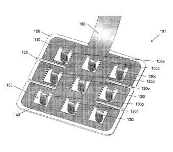
cortical depth
electrodes 130 protruding from the neurological surface probe 101) are
positioned in direct
contact with the neurological target 200. The planar component of the
neurological surface probe
101 remains on the surface of the brain 221. In some surgical procedures the
planar component
of the neurological surface probe 101 remains above the dura mater, while the
cortical depth
probes 130 are below the dura mater. In alternative surgical procedures the
planar component of
the neurological surface probe 101 is below the dura mater, requiring the
formation of a flap of
the dura mater during the surgery. Regardless of the formation of a dural flap
during the surgery,
in most procedures, the cortical depth probes 130 are subdural, and the
microelectrode elements
140 are intended to be in contact with several cortical layers 201.
[0124] In some embodiments, selectable microelectrode elements 140 can be
activated to record
from the neurological target 200. Additionally, recordings of neurological
activity from
microelectrode elements 140 can be used to identify the location or position
of the microelectrode
element 140. For example, a microelectrode element 140 that is recording from
cortical layer
201a will have a different signal than a microelement 140 that is recording
from cortical layer
201b. As an additional example, a microelectrode element 140 that is recording
from cortical
layer 201b will have a different signal than a microelement 140 that is
recording from cortical
layer 201c. In this manner, the physician can determine the positioning of the
microelectrode
elements 140, and the neurological surface probe 101 in the neurological
target 200.
[0125] In some embodiments, the microelectrode elements 140 that are used to
record from the
cortical surface 221 and cortical layers 201 are particularly useful in the
diagnosis of epilepsy.
The recorded activity in the patient can be used to determine the
electrophysiological origin of an
epileptic seizure, and can help the physician decide corrective or surgical
action to be taken. In
many cases the surgeon may recommend a surgical resection. If performed with
this device, the
precision of the resection may be improved and lead to better clinical
outcomes. Additionally, if
the resection is more precise, the patient may be able to keep additional
neurological functionality
that could have been lost to a larger resected area.
-21 -
CA 02782710 2012-06-01
WO 2011/067297 PCT/EP2010/068658
[0126] In some embodiments, selectable microelectrode elements 140 can be
activated to
stimulate a neurological target 200. Additionally, functional outcome of the
neural stimulation
can be used to identify the location or position of the microelectrode element
140 by a clinical
evaluation of the patient undergoing the stimulation. For example, a
microelectrode element 140
that is stimulating a cortical layer 201 in the motor cortex responsible for
right hand index finger
movement will experience twitching and or movement in their right hand index
finger. As an
additional example, a microelectrode element 140 that is stimulating in a
cortical layer 201 in the
auditory lobe may experience the perception of sounds. As an additional
example, a
microelectrode element 140 that is stimulating in a cortical layer 201 in the
visual cortex may
experience the perception of sight. In this manner, the physician can
determine the positioning of
the microelectrode elements 140, and the neurological surface probe 101 in the
neurological
target 200.
[0127] In some embodiments, the microelectrode elements 140 that are used to
stimulate the
cortical surface 221 and cortical layers 201 are particularly useful in the
treatment of stroke. The
stimulation may not create a functional outcome such as movement of limbs, but
may improve
the ease with which patients can move. This stimulation applied to the
microelectrode element
140 may be sub-threshold stimulation, meaning that it will not generate action
potentials in
neurons, but facilitate the ability of a neuron to reach the action potential
threshold, by altering
the extracellular potential.
[0128] In some embodiments, the microelectrode elements 140 that are used to
stimulate the
cortical surface 221 and cortical layers 201 are particularly useful in the
treatment of chronic
pain. The stimulation can be applied to a region of the sensor cortex where
the physician has
concluded that the region may be linked to the patient's pain. For example, a
patient that presents
himself with chronic pain in the face can implanted with the device in the
general region
governing sensation of the face in the sensory cortex. This stimulation can be
applied to the
microelectrode element 140 to suppress pathological activity in order to treat
the pain.
[0129] Referring now to FIG. 4, a schematic of the cortical neuromodulation
device 100 is
provided. The schematic begins with an external controller 170 which the
operator can use to
functions in the device. The external controller 170 can be in direct
electrical contact with the
control circuitry 160, or wirelessly connected through antenna circuitry. The
control circuitry
- 22 -
CA 02782710 2012-06-01
WO 2011/067297 PCT/EP2010/068658
160 is used to translate the commands from the external controller 170 to
stimulate and or record
from the device. The control circuitry 160 is also used to transmit captured
information from the
device to the external controller 170 for display or processing. Subsequently
the control circuitry
is electrical communication with the neurological surface probe 101. The
communication is
preferably through a tether wire or ribbon cable (not shown). Protruding from
the neurological
surface probe 101 are the cortical depth probes 130a through 130n
(collectively 130), where n is
an arbitrary quantity. Furthermore, each cortical depth probe 130 incorporates
at least one
microelectrode elements 140.
101301 Referring now to FIG. 5A, a top view of the exemplary embodiment in
FIG. 1 is
provided. FIG. 5B is a detailed planar view of the control module 150. The
image demonstrates
the curvature of the upper housing 152, and the shape of the lower housing
151. In particular, the
fixation structures 156 are designed in order to be slightly offset from the
planar surface of the
lower housing 151 in order to be adaptable to all skull shapes, curvatures and
sizes.
101311 Referring now to FIG. 6B, an additional perspective view of the
neurological surface
probe 101 is provided. In the image, cortical depth probes 130a through 130c
are the most
proximal. In FIG. 6C, a perspective view of the neurological surface probe 101
is demonstrated
where currents have been applied to a selection of microelectrodes 140.
Microelectrodes that
have a cathodal signal applied to them are labeled 140NEG collectively.
Microelectrodes that
serve as electrical ground are label 14OGND collectively. FIG. 6D demonstrates
the electric field
isosurfaces 141 that the applied currents would create. It is understood by
those skilled in the art
that any combination of signals (anodal, cathodal, ground) can be applied to
any combination of
microelectrodes 140 in order to create an arbitrary, or intentionally
designed, three-dimensional
electrical field in the tissue volume where the neurological surface probe 101
has been implanted.
101321 Referring now to FIG. 6B, an additional perspective view of the
neurological surface
.. probe 101 is provided. In the image, cortical depth probes 130a through
130c are the most
proximal.
101331 Referring now to FIG. 7A, a frontal planar view of the neurological
surface probe 101 is
provided. In the image cortical depth probes 130g through 130i are shown. On
cortical depth
electrode 130i, the microelectrode elements 140 are labeled, 140i a through
140id. The
microelectrode element 140ia is most proximal along the cortical depth probe
130i to the planar
- 23 -
CA 02782710 2012-06-01
WO 2011/067297 PCT/EP2010/068658
surface of the neurological surface probe 101. The microelectrode element
140id is most distal
along the cortical depth probe 130i to the planar surface of the neurological
surface probe 101.
101341 Referring now to FIG. 7B and FIG. 7C, two additional planar views of
the neurological
surface probe 101 are provided. In the image cortical depth probes 130c, 130f,
and 130i are
shown. In FIG. 7B the cortical depth probe 130c is the proximal, whereas the
cortical depth
probe 130i is the most distal.
101351 In FIG. 8A, a detailed perspective view of one cortical depth probe
130g is provided. In
FIG. 8B an additional detailed perspective view of one cortical depth probe
130g is provided.
The microelectrode elements on the surface of the cortical depth probe 130g
are labeled 140ga
through 140gd.
101361 FIG. 9 partially demonstrates how the assembly of the neurological
surface probe is
performed. Additionally, in this example, the cortical depth probes 130 have
not yet been bent
down to protrude from the surface of the neurological surface probe 101. The
supportive backing
layer 120 has been constructed as described above. On its surface are cutouts
of the structure that
will create the cortical depth probe 130 which is here referred to as a
cortical depth probe backing
132. Likewise, on the microelectrode array film 110, a structure referred to
as the cortical depth
probe film 135 is implemented. in this exemplary embodiment, there are nine
cortical depth
probe backings 132 and nine cortical depth probe films 135.
101371 By a process of bonding, the microelectrode array film 110 is attached
to its supportive
backing layer 120. FIG. 10 demonstrates the assembled neurological surface
probe 101 after
bonding, but before the cortical depth probes 130 have been bent down to
protrude from the
planar surface of the neurological surface probe 101.
101381 In use, the cortical neuromodulation device 100 is placed surgically
through a
craniotomy formed in the skull. FIG. 11A is a perspective view of the
placement of the device.
The image demonstrates a cross section of the brain surface 220 and skull 225.
A circular
craniotomy 226 has been performed in the skull. The neurological surface probe
101 has been
surgically placed, with its cortical depth probes 130 piercing the dura mater
(not detailed) and
positioned subdurally. The control module 150 is placed on a different section
of anatomy. It is
surgically placed on the surface of the skull 225 and can be fastened using
cranial screws.
- 24 -
CA 02782710 2012-06-01
WO 2011/067297 PCT/EP2010/068658
FIG. 11B demonstrates an additional perspective view of the cut-away
anatomical region.
FIG. 11C demonstrates an additional planar side view of the cut-away
anatomical region.
101391 In some embodiments, it is preferable to integrate the control module
with the
neurological surface probe into one device, and avoid a wire or ribbon cable
tether. The
additional embodiment of an integrated cortical neuromodulation device 300 in
FIG. 12
demonstrates the integration of all system components into one module.
101401 FIG. 13 demonstrates an additional perspective view of the alternative
embodiment. In
some embodiments, the control circuitry 360 can be directly implemented on the
microelectrode
array film 310. Additionally, in some embodiments, the loop antenna 365 can be
implemented on
the microelectrode array film 310.
101411 FIG. 14 demonstrates a planar view of the integrated cortical
neuromodulation device
300. The cortical depth probes 330 and their respective microelectrode
elements 340 protrude
from the lower surface of the device.
101421 In use, the integrated cortical neuromodulation device 300 is placed
surgically through a
craniotomy formed in the skull. FIG. 15 is a perspective view of the placement
of the device.
The image demonstrates a cross section of the brain surface 321 and skull 325.
A circular
craniotomy 326 has been performed in the skull. The integrated cortical
neuromodulation device
300 has been surgically placed through the craniotomy, with its cortical depth
probes 330
piercing the dura mater (not detailed) and positioned subdurally. FIG. 16
provides an additional
planar view of the placement of the device in a cross section of human
anatomy.
101431 In some embodiments, it is preferable to have a circular neurological
surface probe.
FIG. 17A demonstrates a perspective view of a circular neurological surface
probe 401. The
device incorporates four cortical depth probes 430. On each cortical depth
probe 430 a linear
array of microelectrode elements 440 is implemented. Additionally, a large
surface electrode
430, generally of diameter 3 mm, is used to record EEG signals from the
surface of the brain.
Finally, a ribbon cable tether 480 is used to communicate the microelectrode
elements 440 to a
control module (not shown) as described in previous embodiments. FIG. 17B
demonstrates an
additional perspective view of the circular neurological surface probe 401. In
FIG. 17C, a
perspective view of the circular neurological surface probe 401 is
demonstrated where currents
- 25 -
CA 02782710 2012-06-01
WO 2011/067297 PCT/EP2010/068658
have been applied to a selection of microelectrodes 440. Microelectrodes that
have a cathodal
signal applied to them are labeled 440NEG collectively. Microelectrodes that
serve as electrical
ground are label 440GND collectively. FIG. 17D demonstrates the electric field
isosurfaces 441
that the applied currents would create. It is understood by those skilled in
the art that any
combination of signals (anodal, cathodal, ground) can be applied to any
combination of
microelectrodes 440 in order to create an arbitrary, or intentionally
designed, three-dimensional
electrical field in the tissue volume where the circular neurological surface
probe 401 has been
implanted.
101441 The circular neurological surface probe 401 is implemented by combining
a supportive
backing layer with a microelectrode array film. FIG. 18A demonstrates an
exemplary circular
supportive backing layer 420. It consists of a planar central body from which
four cortical depth
probe backings 432 protrude. Additionally, at the base of each cortical depth
probe backings 432
are bending slits 433 that facilitate the bending of the probe into its final
three-dimensional
construction. FIG. 18B demonstrates the circular microelectrode array film 410
that is used in the
current embodiment. It consists of four cortical depth probe film 435 on which
the
microelectrode elements 440 are disposed. The circular supportive backing
layer 420 and the
circular microelectrode array film 410 are bonded in a process that attaches
them to each other.
Subsequently, the cortical depth probes 430 are bent into place.
[0145] In some embodiments, it is preferable for a circular neurological
surface probe to have a
central cortical depth probe. FIG. 18C demonstrates an additional embodiment
of a circular
supportive backing layer 420C with an additional central cortical depth probe
backing 432CM. It
consists of a planar central body from which four cortical depth probe
backings 432C protrude,
and a central cortical depth probe backing 432CM of the same length and
dimensions projects
from the center of the circular supportive backing layer 420C. Additionally,
at the base of each
cortical depth probe backings 432C are bending slits 433C that facilitate the
bending of the probe
into its final three-dimensional construction. Additionally, at the base of
the central cortical depth
probe backing 432CM are bending slits 433CM that facilitate the bending of the
central probe
into its final three-dimensional construction.
101461 FIG. 18D demonstrates the circular microelectrode array film 410C that
is used in the
current embodiment. It consists of four cortical depth probe films 435C on
which the
- 26 -
CA 02782710 2012-06-01
WO 2011/067297 PCT/EP2010/068658
microelectrode elements 440C are disposed. Additionally, a central cortical
depth probe film
434CM of the same length and dimensions projects from the center of the
circular microelectrode
array film 410C. The circular supportive backing layer 420C and the circular
microelectrode
array film 410C are bonded in a process that attaches them to each other.
Subsequently, the
cortical depth probes are bent into place, with the central cortical depth
probe taking a position
that is normal to the plane formed by the planar section of the supportive
backing layer 420C.
101471 Referring now to FIG. 18E, a perspective view of the circular
neurological surface probe
with central pin 401C is demonstrated. The components demonstrated in FIG. 18C
and FIG. 18D
are assembled to implement this embodiment. It consists of four cortical depth
probes 430C and
a central cortical depth probe 430CM. Microelectrode elements 440C are
disposed on all five
cortical depth probes. The central cortical depth probe 430CM of the same
length and
dimensions as the cortical depth probes 430C project from the center of the
circular neurological
surface probe 401C surface. The circular supportive backing layer 420C and the
circular
microelectrode array film 410C are bonded in a process that attaches them to
each other.
1 5 Subsequently, the cortical depth probes are bent into place, with the
central cortical depth probe
taking a position that is normal to the plane formed by the planar section of
the supportive
backing layer 420C.
101481 Referring now to FIG. 19A a cross-sectional view of a portion of human
brain anatomy
421 is shown, illustrating the exemplary circular neurological surface probe
401 positioned at a
neurological target 422. In general, circular neurological surface probe 401
is representative of
any of the cortical neuromodulation devices described herein. The circular
neurological surface
probe 401 includes an array of microelectrode elements along its individual
cortical depth probes.
Preferably, circular neurological surface probe 401 is implanted using by
performing craniotomy.
Its ribbon cable tether 480 remains outside of the human body, while the
circular neurological
surface probe 401 is implanted on the surface of the cortex of the brain. As
in other
embodiments, individual cortical depth probes are meant to be implanted
subdurally, with the
microelectrode elements in contact with at least one of the subdural layers of
the cortex.
101491 Referring now to FIG. 19B, a planar view of the positioning of the
exemplary circular
neurological surface probe 401 in a portion of human brain anatomy 421
referred to as the
neurological target 422. As illustrated, one or more of the microelectrode
elements circular
- 27 -
CA 02782710 2012-06-01
WO 2011/067297 PCT/EP2010/068658
neurological surface probe 401 are positioned in intimate contact with the
neurological target 422.
One or more additional microelectrode elements of the circular neurological
surface probe 401
may reside at locations not in the immediate vicinity of the neurological
target 422. In at least
some embodiments, one or more of the microelectrode elements are remotely
accessible from a
proximal end of the circular neurological surface probe 401 via one or more
electrically
conductive leads (not shown).
101501 In some surgical procedures it would be highly beneficial to the
patient to have several
circular neurological surface probes 401 implanted in the region of the
neurological target 422K.
FIG. 20A demonstrates a cross-sectional view of a portion of human brain
anatomy 421K,
illustrating four exemplary circular neurological surface probes 401K
positioned at a neurological
target 422K. FIG. 20B is a more detailed close-up view of the neurological
target 422K. Four
circular neurological surface probes 401Ka, 401Kb, 401Kc, 401Kd (collectively
401K) were
implanted in the neurological target 422K. it is highly beneficial in some
surgical procedures to
avoid the sulci 405K on the surface of the brain. The sulci 405K are regions
where the brain
surface folds and may be highly vascularized. The circular neurological
surface probes 401K
each have a ribbon cable tether, collectively 480K, that can lead to the
external portion of the
patient.
101511 In practice the physician will determine how many circular neurological
surface probes
401K should be implanted. In some cases, it might be beneficial to implant
only one, as the
physician might determine that this will provide enough physiological
information, or enough of
a therapeutic stimulation volume. In some cases, it will be beneficial to
implant a multiplicity of
circular neurological surface probes 401 in the region, in order to increase
the probability of
finding the neurological target. The decision to implant a certain quantity of
devices may be
taken before the surgery, using surgical planning software. Alternatively, or
in addition, the
decision can be taken during the surgery.
101521 In some embodiments, it is preferable to integrate the control module
with the circular
neurological surface probe into one device, and avoid a wire or ribbon cable
tether. The
additional embodiment of an integrated circular cortical neuroinodulation
device 401M in
FIG. 21A demonstrates the integration of all system components into one
module. The device
incorporates four cortical depth probes 430M. On each cortical depth probe
430M a linear array
- 28 -
CA 02782710 2012-06-01
WO 2011/067297 PCT/EP2010/068658
of microelectrode elements 440M is implemented. Additionally, a lower housing
451M for
control module is implemented directly above the planar region of the circular
supportive backing
layer 420M. The upper housing 452M is intended to encapsulate the control
circuitry 460M and
loop antenna 465M which are used to control and transmit information to the
integrated circular
cortical neuromodulation device 401M. On the surface of the circular
microelectrode array film
440M are microelectrode array elements 440M which are in communication with
the control
circuitry 460M through embedded conductive traces (not shown). FIG. 21B
demonstrates an
additional perspective view of the integrated circular neurological surface
probe 401M. In this
image, the implementation of an EEG electrode 441M of 3 mm diameter is
visible. FIG. 21C is
an additional planar view of the exemplary integrated circular cortical
neuromodulation device
401M.
[0153] Referring now to FIG. 22, a perspective view of a human brain anatomy
421M is shown
with the exemplary embodiment of the integrated circular cortical
neuromodulation device 401M
implanted in a neurological target 422M. In this exemplary embodiment, the
connection of a
ribbon cable tether the external portion of the patient is not necessary.
However, an external
control module (not shown) is required to communicate with the implanted
device. FIG. 23
demonstrates a more detailed view of the portion of human anatomy 421M and the
positioning of
the exemplary circular neurological surface probe 401M in the neurological
target 422M.
[0154] In some surgical procedures, it would be highly beneficial to the
patient to have several
integrated circular neurological surface probes 401M implanted in the region
of the neurological
target 422M. FIG. 24 is a close-up perspective view of a portion of human
brain anatomy 421M,
illustrating five exemplary integrated circular neurological surface probes
401Ma, 401Mb,
401Mc, 401Md, 401Me (collectively 401M) positioned at a neurological target
422M. It is
highly beneficial in some surgical procedures to avoid the sulci 405M on the
surface of the brain.
The sulci 405M are regions where the brain surface folds and may be highly
vascularized. The
integrated circular neurological surface probes 401M can wirelessly
communicate to the external
portion of the patient.
[0155] In all of the embodiments presented, it is understood that the devices
are meant to be
implanted using a surgical procedure on the surface of the brain.
Additionally, it is intended that
the cortical depth probes which protrude from all embodiments are meant to be
in the subdural
- 29 -
CA 02782710 2012-06-01
WO 2011/067297 PCT/EP2010/068658
region or the brain, and the microelectrode elements on the surface of the
cortical depth probes
are meant to be in contact with at least one of the cortical layers. The
neurological surface probes
are placed on the brain generally for recording and/or stimulation of the
cortex. The region of the
cortex that the physician is target for diagnosis or therapy is termed the
neurological target.
101561 The microelectrode elements can also be placed in other parts of the
body, such as the
retina, the peripheral nervous system for neural recording and/or neural
stimulation of such
portions of an animal anatomy. Although microelectrodes are discussed
generally throughout the
various embodiments, there is no intention to limit the upper or lower size of
the microelectrodes.
The devices and methods described herein are generally scalable, with a
microelectrode size
determined according to the intended application. For at least some of the
neurological
applications, microelectrodes are dimensioned sub-millimeter. In some
embodiments,
microelectrodes are dimensioned sub-micron. In some embodiments, the
microelectrodes are
formed as planar structures having a diameter of about 50 um that are arranged
in a linear array
with center to center spacing of about 100 um. The planar structure of the
microelectrodes can
.. have regular shapes, such as circles, ellipses, polygons, irregular shapes,
or a combination of such
regular and/or irregular shapes.
101571 FIG. 23A is a schematic diagram of one embodiment of a cortical depth
probe assembly.
The microelectrode tip assembly 500 includes a supporting member 502 including
an elongated
portion terminating in a distal tip 506 and a proximal extension 510. A linear
array of three
microelectrode elements 504 is arranged along a longitudinal axis of the
elongated portion of the
support member 502. A corresponding number of three electrode contacts 508 are
located on the
proximal extension 510. Each microelectrode element of the array 504 is
interconnected to a
respective one of the electrode contacts 508 through a respective electrically
conducting lead
trace 512. In the exemplary embodiment, a polymer layer 514 is applied to at
least one surface of
the underlying support member 502. Each of the microelectrode leads, electrode
contacts 508,
and interconnecting lead traces 512 is implemented as an electrically
conducting layer on or
within the polymer layer 514. Although a linear array of microelectrode
elements is shown, other
embodiments are possible with nonlinear, planar, curved surface, and
volumetric (i.e., three-
dimensional) distributions of such microelectrodes are possible.
- 30 -
CA 02782710 2012-06-01
WO 2011/067297 PCT/EP2010/068658
101581 Fabrication Methods
101591 There are several techniques to achieve the microfabricated component
and the required
mechanical and electrical characteristics. The fabrication procedure is a
series of procedural steps
in which various layers are deposited or removed (e.g., etched) to achieve a
final form.
Exemplary sequence of procedural steps is described herein.
101601 Step 1: The carrier wafer and sacrificial layer
101611 In a first step illustrated in FIG. 23A, a carrier substrate 650 is
provided, such as a wafer
composed of a crystalline material, such as Silicon, or an amorphous material,
such as glass, in
particular a thermal shock resistant borosilicate glass commercially available
under the brand
name PYREX , or other suitable smooth supportive material. A first layer 652
comprising at
least two sub-layers is applied to a surface of the wafer 650. One of the sub-
layers 652 is a
sacrificial layer deposited on the wafer 650, which will be removed in a
subsequent
electrochemical etch step. Preferably, the sacrificial sub-layer is preceded
by another sub-layer,
referred to as an underlayer, that will serve to form the electrochemical cell
required to etch the
sacrificial layer. In the preferred embodiment, the sacrificial sub-layer is
Aluminum, or an alloy
of Aluminum such as AlSi, which has a smaller granularity, whereas the
underlayer is a TiW
alloy, Chrome, or similar metal. The sacrificial layer is represented as a
black line 652 in the
image below, the carrier wafer 650 is shown in gray. Each of the images
illustrated in this series
represents a cross section of an exemplary embodiment, and are used herein to
describe the
procedural steps.
101621 In some embodiments, the sacrificial layer 652, in addition to
facilitating
electrochemical removal of the finished device, is to establish a granularity,
or grain size to the
surface of the finished device. Namely, the sacrificial layer can add a micro
or nano-roughness to
the surface that can be precisely controlled at least in part by the selection
of a suitable
.. underlayer. For example, Aluminum can be deposited by DC Sputtering with a
grain size ranging
from 5 nm or less to 600 nm or more. This grain size provides a first grainy
surface. A
polymeric layer is subsequently deposited over the grainy sacrificial layer.
This polymeric layer
can be locally etched in order to create vias that open onto the grainy
sacrificial layer.
Subsequently, a metal layer is deposited over the resulting grainy surface,
and polymeric layer, in
which the deposited metal serves as the neuro-recording /stimulation
microelectrode element, and
-31 -
CA 02782710 2012-06-01
WO 2011/067297 PCT/EP2010/068658
wire trace. The area of the metal that falls into the via in the polymeric
layer forms the
microelectrode surface. The area of the metal falls on the polymeric layer can
be etched into
linear traces and form the interconnect between microelectrodes and bond pads
or circuitry. The
process is described below as a "backside microelectrode." Due to such an
increase in granularity
over a relatively flat surface, the overall surface area of the metal layer
will have a higher
effective surface area than that area subtended by the perimeter of the
element. Beneficially, the
increased surface area results in a corresponding decrease in electrical
impedance of the electrode
element. This concept is important in that it facilitates recording, allowing
a greater recording
fidelity with less complexity due to the reduction in impedance, while
maintaining the same small
diameter that guarantees high localization of the neural activity. An
electrically conducting
surface of an exemplary microelectrode element thus formed is illustrated in
the image of
FIG. 30.
101631 Step 2: Deposition of First Polymeric Layer
[0164] Referring to FIG. 25B, the next step in the fabrication process
includes depositing a first
polymeric layer 654 ¨ sometimes referred to as a resin layer 654. The first
polymeric layer 654
can be deposited upon the sacrificial layer 652. This can be done by any
suitable means known to
those skilled in the art of MEMS processing, by: (i) spin coating a liquid
polymer precursor such
as Polyimide or Silicone precursor; (ii) depositing a polymer through chemical
vapor deposition
as is done with parylene-C; or (iii) laminating a polymer sheet 654 onto the
wafer 650. In some
embodiments, the polymer layer 654 is heated, or baked, to polymerize.
[0165] Referring next to FIG. 25C and FIG. 25D, an optional step includes
etching of first
polymeric layer 654, as may be beneficial when preparing a device having one
or more backside
electrodes, that will ultimately be located along an underside of the finished
device. In this
optional step, the first polymeric layer 654 is locally etched in order to
form open areas 652,
where metals for such backside microelectrodes may be later deposited. This
step is optional, and
unnecessaty when there is no need for any such backside electrodes on the
finished device ¨ all
microelectrode contacts being formed on a front surface of the finished
device. This step is also
advantageous, because the backside electrode metal layer, when included, will
also benefit from
the higher effective surface area that can be gained from the sacrificial
layer's granularity.
- 32 -
CA 02782710 2012-06-01
WO 2011/067297 PCT/EP2010/068658
[0166] The etching can be performed by depositing a mask 656 on the first
polymeric layer 654.
Using well established methods for thin film processing, the mask 656 can be
photolitho-
graphically defined. For example, a photosensitive resin 656 is spin coated
onto the polymeric
layer 654. A process of exposing an unmasked portion of the resin layer 657 to
UV light is used
for those areas in which the operator chooses to remove the polymer layer 654.
The device is
developed in a solvent that will selectively remove only the unmasked areas
657 that were
exposed to UV light. This selective etching process locally opens areas of the
polymeric layer
654, by etching, exposing in this instance the underlayer 652. In some
embodiments, the device
is etched in oxygen plasma to remove the exposed portion of the polymeric
layer 657. The etch
mask 656 may also be removed by the same etching process, but if it is thicker
than the polymer
layer it may not be completely removed. Illustrated in the figures is a
defined etch mask 656.
Alternatively or in addition, the etch mask 656 can also be implemented in a
non-photodefinable
layer, such as Silicon Dioxide deposited by DC Sputtering. The Silicon Dioxide
then has the
photoresist deposited and photolithographically defined on top of it. After
etching the polymeric
layer 654, the Silicon Dioxide mask can be optionally removed.
[0167] FIG. 25D illustrates the device after the exposed portion of the
polymer layer 657 was
removed. As illustrated, a portion of the sacrificial layer 652 is now
exposed. In some
embodiments, the photoresist mask 656 cab be subsequently removed using a
suitable solvent.
[0168] Step 3: Deposition and definition of metal layer
[0169] The deposition of the layer can also be made through a resist mask 670,
as shown in
FIG. 25G. In this case a photoresist mask 686' would be photolithographically
defined on the
polymer layer 654. An electrically conductive (e.g., metal) layer 692' can
then be deposited over
the masked device. Thus, unmasked areas 687 at which it is desirable to have
an electrically
conducting layer 690 formed, are open with respect to the photoresist mask
686', such that the a
portion of the deposited electrically conductive layer 692' lands directly
onto the polymeric layer
654 at the unmasked area 687. This technique is sometimes referred to as a
"lift off' technique.
The photoresist mask 686', with any electrically conductive layer 692'
thereon, is then dissolved,
such that the only remaining metal 690 is on the polymer at the formerly
unmasked areas. Note
that the metal layer 692' on top of the photoresist 686' is also removed by
removal of the
- 33 -
CA 02782710 2012-06-01
WO 2011/067297 PCT/EP2010/068658
photoresist mask 686'. Beneficially, that portion of the electrically
conducting layer 690 in
contact with the polymeric layer 654 remains after removal of the mask 686'.
101701 In an alternative method, referring now to FIG. 25H, a metal layer 692"
can be deposited
onto the entire surface of a wafer 650. As illustrated, the metal layer 692"
is provided on top of
the polymeric layer 654, which is provided on top of the sacrificial layer
652. A masking layer
686" is provided over that portion of the metal layer 692" to remain. Exposed
regions of the
metal layer 692" can then be removed locally by a photolithographic step such
as demonstrated
below.
101711 Referring next to FIG. 25E, an electrically conductive layer that
serves as the electrode
680 and one or more electrically conductive traces 682 is next deposited. Such
an electrically
conductive layer can include a metal layer deposited by any suitable thin-film
process, such as
DC sputtering, RF Sputtering, or evaporation techniques. The metal deposited
in the electrically
conductive layer 680, 682 is preferably platinum, iridium, platinum-iridium
alloy, iridium-oxide,
titanium, or a titanium alloy to ensure acceptable electrical characteristics
(such as charge
transfer) and mechanical strength.
101721 In a preferred embodiment, the metal layer 680, 682 is deposited with
an adhesion
promotion layer in contact with the polymer. For example, titanium can be
sputtered onto the
polyimide layer 654 in an initial partial step to improve adhesion, followed
by a platinum layer
deposited in an intermediate partial step, and optionally, a titanium layer
may them be deposited
onto the platinum layer in a subsequent partial step. This creates a Ti-Pt-Ti
sandwich, where the
titanium is responsible for adhering the platinum to the polyimicle on either
side of it, and the
platinum is the metal layer that will be used.
[0173] For embodiments that produce backside electrodes, as described above in
reference to
FIG. 25C through FIG. 25E, then the electrically conductive layer 680 will be
in contact with the
sacrificial layer 652 in the region of the backside electrode 680. The metal
deposition technique
is selected to ensure that there is contact between the metal on top of the
polymeric layer 654, and
the metal on the exposed portion of the sacrificial layer 652. This is done by
ensuring the metal
680 is conformally deposited, and that the polymeric layer 654 is not too
thick. The metal layer
680 can then be photolithographically defined as explained above. An etch in a
plasma, such as
- 34 -
CA 02782710 2012-06-01
WO 2011/067297 PCT/EP2010/068658
Chlorine gas plasma, can be used to remove the metal layers deposited using a
photoresist mask.
The photoresist mask can then be removed in a solvent.
101741 Step 4: Deposition of 2nd polymeric layer
101751 Referring next to FIG. 251 for a backside electrode embodiment and FIG.
25H, a second
polymeric layer 672, 692 is deposited using a suitable technique, such as any
of the techniques
described above with respect to FIG. 25B. The second polymeric layer 672, 692
is deposited
onto the underlying polymeric layer 654, 664, and any exposed metal layer 658,
668. In some
embodiments, the first polymeric layer 654, 664 can be processed in order to
increase its adhesion
to the second polymeric layer 672, 692. For example, such processing can be
accomplished
through surface roughening or chemical alteration using an oxygen plasma. The
second
insulative, or polymeric layer 672, 692 isolates the electrical traces, when
formed on different
layers with respect to each other. In some embodiments, the polymeric material
can be subjected
to thermal process, such as baking.
101761 Step 5: Definition of polymeric layers
101771 Referring next to FIG. 251 through FIG. 25K, to define the one or more
polymer layers
654, 691 and therefore the device itself, an etch mask 695 is deposited to an
external surface of
the device. This etch mask 695 may consist of a photodefinable resist but
preferably it will be a
hard etch mask such as silicon dioxide or amorphous silicon which can
withstand the etch of the
polymeric layer without significant degradation.
101781 The wafer 650 at this point also has a hard mask 693 deposited, for
example, by DC or
RF sputtering. A photodefinable 695 resist is deposited on the hard mask 693
and the areas of the
polymer 654, 691 that are to be etched are defined.
101791 The hard mask 693 is then etched with a different gas then would be
used to etch the
polymeric layer 654, 691, for example CF4 plasma. Now the one or more
polymeric layer 654,
691 can be etched with a gas, such as oxygen plasma, to the sacrificial layer
652, as shown.
Thus, the remaining portions of the hard mask shown in FIG. 25K define the
extent of the device,
by defining the device's edges 659.
101801 The remaining portions of the hard mask 693 can be optionally removed
in a subsequent
step. The goal of this etching process is to: (i) define the microelectrode
sites; (ii) define the
- 35 -
CA 02782710 2012-06-01
WO 2011/067297 PCT/EP2010/068658
device shape; and (iii) define the contact areas for electronics or wire
attachment. A top view of
an exemplary finished microelectrode device is shown in FIG. 31. A cross-
section of another
exemplary finished microelectrode device is shown in FIG. 32.
101811 If the option of making backside electrodes is taken in step 2, the
device will have
microelectrodes at its surface once removed from the substrate.
101821 Step 6: Optional Bonding of Electronics
101831 If the device is to be integrated with electronics, referring now to
FIG. 25L, the contact
pads 699 can be used at this point to connect to an electrical circuit device
697. For example, an
Integrated Circuit chip 697 can be connected to the contacts 690 (FIG. 25K) by
flip-chip bonding
the chip 697 to the device 661, using a conductive epoxy interlayer. The chip
697 can then be
further attached by chemical bonding, such as an epoxy to ensure a strong and
reliable connection
to the device 661.
101841 Step 7: Removal of Devices from Carrier Wafer
101851 A final step of the fabrication process is illustrated in FIG. 25M, to
remove the device
661, such as a MEMS device, from the underlying wafer 650. The sacrificial
layer 652 (e.g.,
FIG. 25L) is electrochemically etched away. Removal of the sacrificial layer
652 from under the
device 661, frees the underside of the device 661 from the wafer 650. This can
be accomplished
by placing the wafer in a saline bath with a high NaCl concentration. A
platinum electrode in the
bath can be used as a reference. A voltage is applied to the aluminum layer
with respect to the
platinum electrode. The electrochemical cell created by the Aluminum and TiW
etches the
aluminum, and this etch continues below the devices. The devices fall into the
bath and are
removed.
101861 FIG. 26 is a micrograph of an embodiment of a backside microelectrode
element 700.
The image is taken at the process step shown in FIG. 25E. The granularity 702
of the aluminum
sacrificial layer surface 704 is used to increase the effective surface area
of a metal electrode in a
subsequent step. Also shown is a portion of an interconnecting lead 706 in
electrical
communication with the microelectrode element 700.
101871 FIG. 27 is a planar view of a construction element of an embodiment of
a microelectrode
tip. The construction element includes a stencil frame tree 640 including
eight rigid backing
- 36 -
CA 02782710 2012-06-01
WO 2011/067297 PCT/EP2010/068658
members 642 releasably attached to a supporting construction frame 644. Each
of the rigid
backing members 642 includes an elongated portion, and an proximal portion
having an opening
646 to accommodate one or more electronic devices, when fabricated. The
stencil frame tree 640
can be implemented in a rigid material, such that each of the individual
supporting construction
frames can be bonded to the devices on the carrier wafer.
101881 FIG. 28 is a schematic view of a portion of the construction element
illustrated in
FIG. 29, illustrating a close up of the assembled components. In this
exemplary embodiment, the
polymer devices were fabricated using a "backside" electrodes process
101891 FIG. 29 illustrates an exploded schematic view of a construction
element of an
embodiment of a microelectrode array tip. The stencil frame tree 400 is placed
on a surface of a
carrier wafer including micro-array devices 649 formed therein. The stencil
frame tree 400 is
suitably aligned with the micro-array devices 649 of the carrier wafer 648,
and bonded thereto.
One or more electronic devices can be suitably placed on the polymer devices
either after or
before the stencil frame tree 400 is bonded to the carrier wafer 648.
101901 FIG. 30 is a schematic view of another portion of the construction
element illustrated in
FIG. 29. Once the sacrificial layer has been removed as described above, the
devices 649 are
released from the carrier wafer 648 and are now bonded to the stencil 640 for
support. In the
exemplary embodiment, the side of the polymeric device 649 facing the carrier
wafer 648 (and in
contact with the sacrificial layer) has the microelectrodes at its surface. In
general,
microelectrodes may be included in either or both sides as described herein.
101911 In some embodiments, a rigid back 642 on the polymer micro-device 649
is required.
This renders the device 649 fully, or locally, rigid. This rigidity might be
advantageous for
insertion into tissue. The concept is a stencil shape 640 which can be bonded
onto the devices on
the carrier wafer where they have been fabricated. The stencil shape 640 can
be implemented in a
polymer, such as PEEK or Polyurethane, or in metal such as Medical Grade
Stainless Steel or
Titanium. It can be molded into shape, cut by machining or laser, or stamped
out. When this
rigid structure has been attached to the devices, the electronic chip can be
bonded. The electronic
chip can also be bonded to the devices beforehand. After the assembly process
the devices can be
removed from the carrier wafer using the same sacrificial etching techniques
as described above.
A further assembly procedure can be to remove the rigid backing from its frame
and integrate the
- 37 -
CA 02782710 2012-06-01
WO 2011/067297 PCT/EP2010/068658
device with its final structure. In some embodiments, the rigid backing is
conductive. In other
embodiments, the rigid backing is non-conductive. When this support structure
is of a conductive
material, it can also serve as the electrical ground or reference for the
stimulation.
101921 FIG. 33A through FIG. 36C are images of additional embodiments, in
which one or
more backing layers are used to support a microelectrode film. The one or more
backing layers
can be rigid, or semi-rigid. In some embodiments, the one or more backing
layers can be flexible
FIG. 33A illustrates a planar view of a construction element used to create a
rectangular array of
microelectrode tips. The exemplary construction element includes a stencil
frame tree 740'
including an arrangement of, in this example, twelve individual semi-rigid
backing members 742.
The stencil frame tree 740' can include a rigid material, such as medical
grade stainless steel. In
some embodiments, the stencil frame tree 740' can be bonded to one or more
microelectrode
devices, for example, on a carrier wafer.
101931 The stencil frame tree 740' can be implemented by laser cutting, water-
jet cutting,
chemical etching using photosensitive masks, or another method used to obtain
medical-grade,
two-dimensional structures. The stencil frame tree 740' can include one or
more, open-ended or
enclosed, apertures 746, for example, in which microelectronic circuitry can
be located.
101941 The stencil frame tree 740' is also characterized by its overall shape
and size.
Generally, any overall shape is contemplated, including polygons, ellipses,
circles, serpentines,
irregular shapes, and any combination of such shapes. In the illustrative
embodiment, a
substantially rectangular stencil frame tree 740' is characterized by its
width, W, and its length, L.
In the exemplary embodiment, the width is 20 mm, and the length is 15 mm. The
stencil frame
tree 740' is generally thin to facilitate fabrication and placement within the
body. In the
exemplary embodiment, the thickness is about 0.1 mm (not shown). Generally,
the stencil frame
tree 740' has an overall shape and dimensions conforming to the anatomy for
which it is meant to
be used. Such target anatomies include any of the anatomies described herein,
including the
brain, the spine, the peripheral nerve system, the cochlea, the retina, and
other parts of the body.
In some embodiments, it may have a width as wide as 20 cm or greater, and a
length as long as
15 cm or greater, although no general limitation as to size and shape are
contemplated.
101951 FIG. 33B is a perspective view of a portion of the stencil frame tree
740, illustrating
several semi-rigid backing members 742 formed therein. The general shape semi-
rigid backing
- 38 -
CA 02782710 2012-06-01
WO 2011/067297 PCT/EP2010/068658
members 742 can be formed by any suitable means, including pushing, molding,
or stamping.
Once formed, the semi-rigid backing members 742 can be bent or otherwise
formed into a
downwards position as shown in FIG. 33C. In other embodiments, the backing
members 742 can
be bent into an upward position, or into a combination of downward and upward
positions. This
.. action results in protruding portions forming a supportive, probe backing
member 743. As
mentioned in previous embodiments, this bending can be performed before, or
after, a
microelectrode film has been attached to the stencil frame tree 740'.
101961 FIG. 34A and FIG. 34B demonstrate additional embodiments of a stencil
frame tree
740", 740" (generally 740). In some embodiments, the stencil frame tree 740
can include one or
more, vertical elongated grooves or openings 745a through 745c (generally 745)
in order to make
the stencil frame tree 740 more flexible along one or more axes, enabling a
generally planar
structure to conform to a portion of anatomy that is not flat, as shown in
FIG. 34A. In some
embodiments, the stencil frame tree 740 can include one or more, horizontal
746 or vertical
elongated grooves or openings 745, in order to make it more flexible along
several axes, enabling
it to conform to a portion of anatomy which is not flat, as shown in FIG. 34B.
101971 FIG. 34C and FIG. 34D demonstrate various embodiments of semi-rigid
backing
members 742, illustrating different shapes and features. FIG. 34C demonstrates
a closer view of
the embodiment discussed above, characterized by a relatively sharp tip which
can promote easier
penetration of tissue, including the dura mater on the surface of the brain.
The rigid members
742, 747 are also characterized by their respective length d measured from a
base portion to the
tip, that can be implemented to be short, or long enough to reach certain
areas of anatomy. In
some embodiments, one or more of the semi-rigid backing members 742, 747 of
the same stencil
frame tree 740 can have different dimensions and/or different shapes. In some
embodiments,
e.g., for cranial applications, the length d is generally about 1-4 mm but can
be as short as 0.5 mm
or less, or as long as several centimeters or greater.
101981 FIG. 34D illustrates an additional embodiment, characterized by a
rounded tip which can
prevent chronic injury of tissue after implantation. The rigid member 747 also
differs by an
aperture, or gap in its base 748 which can improve the ease of bending the
member into is final,
protruding position. Such a gap 748 can be included in any of the embodiments
described herein.
- 39 -
CA 02782710 2012-06-01
WO 2011/067297 PCT/EP2010/068658
101991 FIG. 35A illustrates a top perspective view of an assembled
microelectrode assembly
750 that can be used for recording and/or stimulation. In this assembly the
rigid stencil frame tree
740' is supporting a microelectrode film 755 (not shown) on its inferior side.
Semi-rigid backing
members 742 have been bent downwards to protrude from its inferior side. A
microelectronic
circuit element 752 is electrically coupled between the microelectrode film
and an external device
(not shown) through flexible electric conduit member 754.
102001 FIG. 35B illustrates in more detail a perspective view of a single
rigid backing member
742 from the inferior side of the assembly 750. The microelectrode film 755 is
visible, having
been bonded to the inferior side. On the inferior side of the microelectrode
film 755 are an
.. arrangement of microelectrode elements 765. The microelectrode film 755 and
microelectrode
elements 765 conform to the bent rigid backing member 742, extending away from
the plane of
the stencil frame tree 740'. On the surface of the exemplary embodiment are
four microelectrode
elements or sites 765. These sites can also be used for one or more of sensing
or recording neural
activity, or electrical stimulation, or they can be enabled to stimulate and
record from the same
site. The number of microelectrode sites 765 of each bent rigid backing member
742 can vary
from one or more. In this exemplary embodiment there are four microelectrode
stimulation sites
765. They can also be arranged in other configurations, including any of the
configurations
described herein, such as a tetrode configuration as will be shown in
subsequent embodiments,
such as in FIG. 42A through FIG. 42D and FIG. 43F through FIG. 43G.
102011 FIG. 35C illustrates a perspective view of an assembled microelectrode
recording and
stimulation device 780. In this assembly the rigid stencil frame tree 790 is
supporting a
microelectrode film 795 on its inferior side. Semi-rigid backing members 792
have been bent
downwards to protrude from its inferior side. A microelectronic circuit
element 782 brings the
microelectrode film into electrical contact with an external device (not
shown) through flexible
electric conduit member 784.
102021 FIG. 35D illustrates a closer perspective view of a single rigid
backing member 792
from the inferior side of the assembly 780. The microelectrode film 795 has
been bonded to the
superior side of the rigid stencil frame tree 790. The microelectrode film 795
can be
implemented using the micro-fabrication processes described herein, and can be
bonded to the
.. rigid stencil frame tree 790 by gluing or heating. On the superior side of
the microelectrode film
- 40 -
CA 02782710 2012-06-01
WO 2011/067297 PCT/EP2010/068658
795 are microelectrode elements 796 and 797 which conform to the bent rigid
backing member
792. On the surface is a relatively large microelectrode stimulation site 796
for stimulating neural
activity. Additionally, on the surface is an arrangement of four relatively
small microelectrode
recording sites 797 arranged in a tetrode configuration used for single neural
cell recording. The
number of microelectrode stimulation sites 796 on each rigid backing member
792 can vary from
one or more. There are further tetrode configuration as will be shown in
subsequent
embodiments, such as in FIG. 42A through FIG. 42D and FIG. 43F through FIG.
43G.
102031 FIG. 35E illustrates a perspective view of the array of protruding
microelectrode
elements 762 shown in FIG. 35A. The microelectrode film 755 can be implement
using any of
the microfabrication procedures previously described. In this exemplary
embodiment, the
backside fabrication process was used. The microelectrode film 755 can be
bonded to the stencil
tree frame through gluing or heating.
102041 As shown in FIG. 34A and FIG. 34B, it may be necessary to include
elongated gaps in
the rigid backing frame 740 and the bonded microelectrode film 755 in order
for the
microelectrode assembly 750 to conform to a portion of anatomy. FIG. 36A shows
a portion of
human anatomy, the left hemisphere of the brain 771. On its cortical surface,
an exemplary
microelectrode assembly 750 has been placed, which can be used to record
and/or stimulate
neural activity.
102051 FIG. 36B illustrates an additional perspective demonstrating both the
left hemisphere
771 and the right hemisphere 772 of the brain. The microelectrode assembly 750
has been
surgical placed on the cortex, and connected to a separate control system (not
shown) through
electrical conduit 754. The separate control system can be located within the
body, external to
the body, or a combination of internal and external. The device is generally
placed by creating a
craniotomy. The protruding rigid members 742 can puncture the dura mater (not
shown)
therefore not requiring its surgical removal. Alternatively or in addition, a
surgeon will remove
the dura mater, and the protruding members 742 will puncture the cortex with a
depth that is
determined by the length of the protruding member 742.
102061 This is demonstrated in more detail in FIG. 36C, in which an array of
12 protruding
members 742 have been inserted into the first layers of the cortex. A
microelectronic element
752, when included, can be used to record, stimulate, or both record and
stimulate neural activity
-41 -
CA 02782710 2012-06-01
WO 2011/067297 PCT/EP2010/068658
on each of the microelectrode sites that have been implemented on each of the
protruding
members 742. In some embodiments, one or more of the protruding members 742
can be
actuated independently or in one or more groupings to record and/or stimulate
a desired region
addressable by the device 250. In general, the microelectrode assembly 750 can
be configured
with any of microelectrode probe described herein, and used in combination
with any of the
stimulation and/or recording or sensing devices described herein.
[0207] Electronic Components
[0208] The electronic components of the device enable: (i) recording of neural
activity from
the microelectrode array to identify which microelectrode sites are closest to
the stimulation
region of interest; and (ii) stimulation and modulation of neuronal activity
with the
microelectrode array and the ability to select which microelectrode sites
stimulating.
[0209] The electronics can be implemented using discrete components,
integrated circuit
technology, or a combination of both. A black box design of the electronics is
shown below. The
electronics can be driven by an existing Implantable Pulse Generator (IPG),
but will include a
telemetric programming interface to properly condition or route the signal
from the IPG to the
microelectrode array. An embodiment of the electronic components exists which
does not require
the IPG.
[0210] Mechanical Components
[0211] The mechanical components and associated assembly processes serve to
house the
device in a hermetic and biocompatible manner. They also enable connection to
an existing
Implantable Pulse Generator or the extra-corporeal control unit. The extra-
corporeal unit
provides power, programming ability and retrieval of information. It can be
implanted much like
the external cochlear stimulation systems that exist today. In an embodiment
that includes an
Implantable Pulse Generator, it would serve to retrieve information and
program the electrical
unit to route the signals from the IPG to the microelectrode array.
102121 Referring to FIG. 37, a functional block diagram of an exemplary
embodiment of a
neurological target stimulator 820 configured in a stimulation mode. The
stimulator 820 includes
an implantable portion 822 including a microelectrode array 826 positionable
at a neurological
target. The implantable portion 822 also includes a signal generation device
828 for actively
- 42 -
CA 02782710 2012-06-01
WO 2011/067297 PCT/EP2010/068658
stimulating the neurological target. In some embodiments, each of the one or
more
microelectrodes of the microelectrode array 826 is in communication with a
dedicated signal
generation device 828. The respective stimulation signal provided at an
optimized frequency for
each individual microelectrode-tissue interface, based on a peak resistance
frequency. The
implantable portion 822 can include a power source 832, such as a battery. In
some
embodiments, the implantable portion 822 also includes a telemetry and control
module 834
configured for external communication with an extra-corporeal unit 824. Such a
feature can be
used to provide extra-corporeal control for operating the implantable portion
822.
102131 Referring to FIG. 37, a functional block diagram of another exemplary
embodiment of a
neurological target stimulator 840 is illustrated configured in so-called
routing mode. The
stimulator 840 includes an implantable portion 842 including a microelectrode
array 846
positionable at a neurological target. The implantable portion 842 also
includes a signal routing
circuit 850 configured to direct a stimulation signal to one or more of the
microelectrodes 846 for
actively stimulating the neurological target. In this embodiment, the
stimulation signal is
obtained from a separate, implantable pulse generator 857. The pulse generator
857 is in
communication with the implantable portion 842 through an interconnection
cable 856 containing
one or more signal leads. The implantable portion 842 also includes at least
one signal
conditioner 848 configured to condition an output signal from the pulse
generator 857 suitable for
stimulation of the neurological target through one or more of the
microelectrodes 846. The
implantable portion 232 generally includes a power source 852, such as a
battery. In some
embodiments, the implantable portion 842 also includes a telemetry and control
module 854
configured to communicate with an extra-corporeal unit 844, to provide
controls for operating the
implantable portion 842.
102141 Filtering of an Existing Signal.
102151 In some embodiments, the signal conditioner 848 include a filtering
circuit to pre-filter
or gain adjust (e.g., pre-amplify and/or attenuate) or otherwise condition an
existing signal before
routing it to a microelectrode array. Several popular filter options include
digital filters, such as
infinite impulse response (JIR) filters, electronic filters using one or more
electrical components,
such as inductors and capacitors, and surface acoustic wave (SAW) devices. The
filters can be
designed through well known filter synthesis techniques to have a preferred
performance features.
- 43 -
CA 02782710 2012-06-01
WO 2011/067297 PCT/EP2010/068658
Some of the controllable features in filter synthesis include filtration
bandwidth, corner
frequency, pass-band ripple, and relative sideband level. Such filters include
categories referred
to as Butterworth, Chebyshev 1 and 2, and Elliptic filters. The particular
implementation ¨
whether analog or digital, passive or active, makes little difference as the
output from any
implementation would still match the desired output.
102161 FIG. 39 is a functional block diagram of another embodiment of a
neurological
microelectrode target stimulator 814 is shown. The stimulator 814 includes a
microelectrode
array 815 positionable at a neurological target of interest. The stimulator
814 also includes an
impedance analyzer 816 configured for measuring an electrical impedance, a
preferred frequency
detector 817, and a stimulator 818 for electrically stimulating the
neurological target.
[0217] The impedance analyzer 816 can use any of various known techniques for
measuring
electrical impedance. Generally, the impedance analyzer 816 provides a test
electrical signal
having known or measurable attributes to the microelectrode-tissue interface.
Such attributes
include a voltage level of a voltage source, or a current level of a current
source. The test voltage
or current, as the case may be, when applied to the microelectrode-tissue
interface, induces a
sensed current or voltage according to physical properties of the
microelectrode-tissue interface.
The impedance analyzer 816 can form a ratio of the test signal to the sensed
signal, yielding an
impedance value according to Ohm's Law: Z=V/I. As the microelectrode-tissue
impedance Z is
a complex quantity, each of the test and sensed electrical signals is
identified as having both a
magnitude and a phase.
102181 In operation, the impedance analyzer measures a complex impedance of
the
microelectrode-tissue interface surrounding the at least one microelectrode
815. The impedance
analyzer repeats the measurements at multiple different frequencies, by
varying frequency of the
applied test electrical signal. Preferably, the multiple frequencies span a
frequency range that
includes biologically relevant frequencies. The preferred frequency detector
817 identifies the
measured impedance being closest to a pure resistance. Such a determination
can be
accomplished by identifying the measured impedance value having a phase value
closest to zero.
For example, a measured impedance can be identified having minimum absolute
value phase (i.e.,
MIN ZZ ). Such a determination can also be accomplished by identifying the
measured
impedance value having a minimum reactance (i.e., MIN(ImIZI)). The frequency
at which the
- 44 -
CA 02782710 2012-06-01
WO 2011/067297 PCT/EP2010/068658
impedance determined to be closest to a pure resistance is identified as a
preferred stimulation
frequency. The stimulator 818 is then adjusted to provide a stimulation signal
at a frequency, or
frequency band, at or near the preferred stimulation frequency. The
stimulation signal is then
applied to the micro electrode array 815.
102191 Illustrated in FIG. 40 is an electronic circuit schematic diagram for
an exemplary on
board ASIC as shown in the embodiments above. Shown along the right hand
portion of the
schematic diagram are eight stimulation electrode elements 968a through 968h
(generally 968)
which are generally spread between several cortical depth probes. Each one of
these elements
968 is in electrical communication with a respective electronic device contact
974a through 974d
and 974m through 974p (generally 974). Also illustrated along the right hand
portion of the
schematic diagram are eight recording electrode elements 969a through 969h
(generally 969).
Similarly, the recording contacts are spread between several cortical depth
electrodes. Similarly,
each of the recording electrode elements 970 is in electrical communication
with a respective
electronic device contact 974e through 974h and 974j through 9741. For
illustrative purposes, the
schematic diagram includes a representative electronic device 980. For
brevity, the schematic
diagram includes only eight recording and eight stimulation contacts but a
full schematic diagram
for many more contacts is similar. Additionally, or alternatively, some
embodiments will only
include recording electrodes. Additionally, or alternatively, some embodiments
will only include
stimulation electrodes. The electronic device may include one or more of a
switch or router, a
preamplifier, a signal conditioner, a multiplexer, and a controller. The
electronic device 980 is in
electrical communication with all sixteen of the electronic device contact
elements 974a through
974p.
102201 The electronic device 980 is in further communication with wire lead
contacts 976a
through 976d (generally 976) that are embedded in the exemplary ribbon cable
tether. In the
illustrative example, the first wire lead contact 976a is used for supplying
electrical power to the
microelectronic device and/or one or more of the stimulation electrode
elements 968. The second
wire lead contact 976b is used to provide an electrical ground contact. This
ground contact 976b
may include earth ground, another electrical ground within the system, such as
a chassis ground
of a medical device connected to the electronic device 980, or simply a signal
return line. A third
wire lead contact 976c corresponds to a control signal that may be used to
provide control inputs
- 45 -
CA 02782710 2012-06-01
WO 2011/067297 PCT/EP2010/068658
from an operator or other medical device, to control configuration and/or
operation of the
electronic device 980. Alternatively or in addition, the control signal
contact 976c may be used
for control signals from the electronic device 980 to another medical device.
A fourth wire lead
contact 976d corresponds to a signal contact as may be used for directing
electrical activity
detected by one or more of the recording electrode elements 969 to a recording
or display device.
Alternatively or in addition, the signal contact 976d may be used for
directing electrical
stimulation signals from another medical device to one or more of the
stimulation electrode
elements 968.
[0221] A top view of an exemplary embodiment of a microelectrode assembly 920
is illustrated
in FIG. 41A. The assembly 920 includes an array of microelectrodes 922
positioned along a
distal end of an elongated probe substrate 924. A first electronic assembly
928 is positioned at a
proximal end of the elongated probe substrate 924. The first electronic
assembly 928 can include
one or more integrated circuit elements 921, such as a microprocessor, and one
or more discrete
electronic components 932. The first electronic assembly 928 is interconnected
to each of the
microelectrodes 922 through a respective trace 926 running along the elongated
probe substrate
924. The electronic assembly 928 and can be configured to implement one or
more functions of
the implantable neurological stimulator described herein. In some embodiments,
the elongated
probe substrate also includes at least a portion of the electronic assembly
928.
[0222] In some embodiments, the first electronic circuitry 928 is connected to
an implanted
pulse generator (not shown) through a cable 924. In some embodiments, as
shown, a second
electronics assembly (or a portion of the first electronics assembly) includes
telemetry circuitry
939, such as a telemetry antenna. In the exemplary embodiment, at least a
portion of electronic
circuitry 928, 938 is positioned adjacent to the microelectrodes 922, for
example being joined by
the elongated probe substrate 924.
[0223] The mechanical components and associated assembly processes serve to
house the
assembly 920 in a hermetic and biocompatible manner. They may also enable
connection to an
existing Implantable Pulse Generator or the extra-corporeal control unit. The
extra-corporeal unit
can provide power, programming ability, and retrieval of information. In some
embodiments, the
assembly 920 can be implanted much like currently available external cochlear
stimulation
systems. In an embodiment that includes an implantable pulse generator, it
would serve to
- 46 -
CA 02782710 2012-06-01
WO 2011/067297 PCT/EP2010/068658
retrieve information and program the electrical unit to route the signals from
the implantable
pulse generator to the microelectrode array 922.
102241 The device provides highly localized and efficient stimulation by
incorporating
microfabricated components, electronic components and mechanical components.
The
microfabricated component consists of a microelectrode array. This array can
be implemented in
a polymeric material such as polyimide, polyurethane, parylene, or
polysiloxane (silicone) and
includes thin film or plated layers of a metal or metal oxide with high charge
transfer capability
such as platinum, platinum-iridium, iridium, iridium oxide or titanium. The
polymeric and
metallic layers can be deposited sequentially and formed using established
principles of
microfabrication such as spin coating, DC/RF sputtering, photolithography,
plasma etching, and
etching with a mask consisting of a secondary or sacrificial material such as
silicon dioxide or
photosensitive resist. The metallic layer can be formed to create the
microelectrode arrays and
traces which connect the array to the electronics and housing. The polymeric
layers serve to
isolate the traces from each other but also provide the structure of the
implant's
stimulating/recording tip. There are several fabrication methods which can be
described to build
such a microfabricated component.
102251 The electronic or microelectronic components of the device enable: (i)
the ability to
identify the peak resistance frequency for each individual microelectrode site
using electrical
impedance spectroscopy; (ii) stimulate at the characteristic peak resistance
frequency of each
microelectrode (this guarantees minimized signal distortion and maximum charge
transfer to the
tissue); and (iii) stimulation and modulation of neuronal activity with the
microelectrode array
and the ability to select which microelectrode sites are stimulating.
102261 The electronics can be implemented using discrete components,
integrated circuit
technology, digital signal processing (DSP), or a combination of all three.
The electronics can be
incorporated in one unit, or can be used in conjunction with an existing
implantable pulse
generator (IPG). The electronics may include a telemetric programming
interface to properly
condition or route the signal from the IPG to the microelectrode array.
102271 Referring to FIG. 41B, a side view of an exemplary alternative
embodiment of a
rnicroelectrode structure is illustrated. In this embodiment, an electronics
assembly 956 is
positioned remote from the microelectrode array 952. The microelectrode array
952 is joined to
- 47 -
CA 02782710 2012-06-01
WO 2011/067297 PCT/EP2010/068658
the electronics assembly 956 through an arrangement of interconnecting
electrical leads 954. The
electronics assembly 956 can be configured to implement one or more functions
of the
implantable neurological stimulator described herein. As illustrated, the
electronics assembly 956
can also be connected to an implanted pulse generator (not shown) through an
interconnecting
.. cable 960. Alternatively or in addition, the electronics assembly 956 can
include telemetry
circuitry for communicating with an external telemetry device 962.
102281 The electronics assembly can include an electrical grounding lead for
interconnection to
an electrical ground potential 958. In any of the embodiments described
herein, impedance
measurements and/or stimulation can be implemented between two or more
microelectrodes (e.g.,
adjacent microelectrodes). Alternatively or in addition, impedance
measurements and/or
stimulation can be implemented between one or more microelectrodes and an
electrical ground
reference.
102291 Note that a device can be assembled to not include electronics. This
device would then
transfer the signal from the Implantable Pulse Generator directly to the
electrodes. A device with
.. electronics would first "pre-filter" the signal before applying to the
electronics. This "pre-filter"
might take the form of signal filtering in order to achieve a certain signal
spectrum, multiplexing
and routing in order to direct signals from a pulse generator to a choice of
microelectrode sites.
The following figures demonstrate the different components and embodiments.
102301 Cortical Depth Probe Embodiments
102311 Various exemplary embodiments of microelectrode array element
configurations
including tetrode arrangements are illustrated in FIG. 42A through FIG. 42D.
Referring to
FIG. 42A, a microelectrode array element 1000 includes a stimulation electrode
1002 and four
recording electrodes 1004. In the exemplary embodiment, the stimulation
electrode 1002 is disc-
shaped; however, other shapes are anticipated, such as polygons, ovals, and
irregular shapes. In
this embodiment, the recording electrodes 1004 are substantially smaller than
the stimulation
electrode 1002, and positioned within the outer perimeter of the stimulation
electrode 1002. In
order to accommodate this arrangement, the stimulation electrode includes a
respective open area
1006, one for each of the recording electrodes. In the exemplary embodiment,
the recording
electrodes 1004 are uniformly spaced having about 90 angular separation
between adjacent
pairs.
- 48 -
CA 02782710 2012-06-01
WO 2011/067297 PCT/EP2010/068658
[0232] In general, the open areas 1006 can have any shape, and the shape need
not be the same
as the shape of any recording electrode 1004 that may be positioned therein.
In the exemplary
embodiments, the open areas 1006 do have a similar shape, namely a circle, as
the disc-shaped
recording electrodes 1004. The openings are dimensioned larger than the
recording electrodes
1004, such that the recording electrodes can be placed within the open areas
1006, without
touching the stimulation electrode 1002. An annular region of separation
exists between the two
electrodes 1002, 1004. The recording electrodes 1004 may each be similarly
shaped and/or
similarly sized with respect to each other. They may have similar shape as the
stimulation
electrode 1002, or have a different shape. In some embodiments, at least some
of the recording
1 0 electrodes 1004 have different shapes and/or different sizes with
respect to each other.
102331 In the exemplary embodiment, the four disc electrodes 1004 embedded
within the larger,
stimulation electrode 1002. The recording electrodes 1004 each have a
respective diameter of
about 50 p.m, and a relative separation to their nearest neighbors of about
150 p.m. The
stimulation electrode has a diameter of 300 Rm. In some embodiments, the
diameter of each
recording electrode can range between about 2 tim or less, and about 300 tim
or more. In some
embodiments, the diameter of the stimulation electrode can range between about
5 pm or less,
and about 1,000 rim or more.
[0234] Referring to FIG. 42B, an alternative embodiment of a microelectrode
array element
1010 shows a stimulation electrode 1012 as a non-closed disc. The outer
perimeter of the
stimulation electrode 1012 generally follows a circular arc, with indentations
defining open areas
1016 extending in from the perimeter, towards the center of the electrode
1012. In particular,
four such open areas 1016, or slots, each accommodate a respective recording
electrode 1014.
The recording electrode 1014 is positioned toward an inner end of the open
area 1016, nearest the
center of the stimulation electrode 1012. In at least some embodiments, the
recording electrode
1014 is spaced apart from a perimeter of the open area 1016, such that the
recording electrode
1014 does not touch the stimulation electrode 1012. In some embodiments, the
perimeter of the
stimulation electrode 1012 are generally rounded, without sharp corners, in
order to prevent
highly localized fields. Although a four-recording electrode embodiment is
shown, other
embodiments are possible including one or more recording electrodes positioned
within
respective open areas 1016. Although circular shapes are illustrated for each
of the stimulation
- 49 -
CA 02782710 2012-06-01
WO 2011/067297 PCT/EP2010/068658
electrode and the recording electrode, different shapes can be used. The
shapes can be regular,
such as ellipses, polygons, and irregular shapes.
102351 Referring to FIG. 42C, illustrates a similar embodiment of a
microelectrode array
element 1020 to that described above, except that two tetrodes 1024a, and
1024b are embedded
within the same stimulation electrode 1022. The two tetrodes 1024a, 1024b can
record neural
activity from different tissue volumes sizes, with different sensitivities to
neural activity. The
"inner tetrode" 1024b can have the same, or different microelectrode diameters
than the "outer
tetrode" 1024a. The diagram shows an "inner tetrode" with 50 p.m discs, and an
"outer tetrode"
with 60 tim discs. Other shapes, sizes, and numbers of tetrode elements are
possible.
102361 Referring to another microelectrode element embodiment 1030 illustrated
in FIG. 42D, a
tetrode 1034 is only slightly embedded into the stimulation electrode 1032. As
shown, the
innermost portion of the open area 1036 is spaced apart from an outer
perimeter of the stimulation
electrode 1032 by a distance less than a diameter of the recording element
1034. Such a
configuration would allow adjustment and optimization of the sensitivity and
volume of tissue
being recorded.
102371 Various embodiments of neurological stimulation devices and techniques
have been
described herein. These embodiments are given by way of example and are not
intended to limit
the scope of the present disclosure. It should be appreciated, moreover, that
the various features
of the embodiments that have been described may be combined in various ways to
produce
numerous additional embodiments.
102381 One or more of any of the microelectrode array elements 1000, 1010,
1020, 1030 can be
positioned on an elongated planar member, or a cortical depth probe, forming a
microelectrode
array film that is one component of a neurological surface probe. The
neurological surface probes
described above were composed of at least one cortical depth probe. In most
embodiments the
cortical depth probe protrudes from a planar surface of the neurological
surface probe. It is
understood that the following embodiments, i. e. , FIG. 43A through 43J, of
cortical depth probes,
can each be used and implemented in the embodiments of neurological surface
probes presented
herein.
- 50 -
CA 02782710 2012-06-01
WO 2011/067297 PCT/EP2010/068658
102391 A series of exemplary cortical depth probes are illustrated in FIG. 43A
through
FIG. 43J. An exemplary cortical depth probe 1040 is illustrated in FIG. 43A.
The cortical depth
probe 1040 includes four microelectrode elements 1045. Each of the
microelectrode elements
1045 can be used as stimulation or recording electrodes, or combined
stimulation-recording
electrodes. In the present embodiment microelectrode elements 1045 are
implemented with a
diameter of 300 um and are spaced by 1 mm. In the illustrative embodiment, the
microelectrode
elements 1045 are discoid and are spaced apart from each other in a manner to
cover a wide linear
depth in the cortical region.
102401 A series of exemplary cortical depth probes are illustrated in FIG. 43A
through
FIG. 43J. An exemplary cortical depth probe 1040 is illustrated in FIG. 43A.
The cortical depth
probe 1040 includes four microelectrode elements 1045. Each of the
microelectrode elements
1045 can be used as stimulation or recording electrodes, or combined
stimulation-recording
electrodes. In the present embodiment microelectrode elements 1045 are
implemented with a
diameter of 300 p.m and are spaced by 1 mm. In the illustrative embodiment,
the microelectrode
elements 1045 are discoid and are spaced apart from each other in a manner to
cover a wide linear
depth in the cortical region.
102411 An additional cortical depth probe 1050 is illustrated in FIG. 43B. The
cortical depth
probe 1050 includes three microelectrode elements 1055. Each of the
microelectrode elements
1055 can be used as stimulation or recording electrodes, or combined
stimulation-recording
electrodes. In the present embodiment microelectrode elements 1055 are
implemented with a
diameter of 400 um and are spaced by 1.5 mm. In the illustrative embodiment,
the
microelectrode elements 1055 are discoid and are spaced apart from each other
in a manner to
cover a wide linear depth in the cortical region.
102421 An additional cortical depth probe 1060 is illustrated in FIG. 43C. The
cortical depth
probe 1060 includes two small diameter microelectrode elements 1065 and two
large diameter
microelectrode elements 1066. Each of the microelectrode elements 1065 and
1066 can be used
as stimulation or recording electrodes, or combined stimulation-recording
electrodes. However,
in the present embodiment it may be preferable to use the small diameter
microelectrode elements
1065 as recording electrodes because they are smaller in diameter and may
capture more single-
unit cellular activity. Additionally, it may be preferable to use the large
diameter microelectrode
-51 -
CA 02782710 2012-06-01
WO 2011/067297 PCT/EP2010/068658
elements 1066 as stimulation electrodes because they are larger in diameter
and can transfer more
charge to the neural tissue increasing the efficacy of stimulation. In the
present embodiment,
small diameter microelectrode elements 1065 are implemented with a diameter of
300 um, and
large diameter microelectrode elements 1066 are implemented with a diameter of
700 pm. The
microelectrode elements 1065 and 1066 are spaced by 1.2 mm. In the
illustrative embodiment,
the microelectrode elements 1065 and 1066 are discoid and are spaced apart
from each other in a
manner to cover a wide linear depth in the cortical region.
102431 Another alternative embodiment of a cortical depth probe 1070 is
illustrated in
FIG. 43D. In this embodiment, each of the cortical depth probes 1070 include
at least one
elongated microelectrode elements 1075. Each of the elongated microelectrode
elements 1075
can be used as stimulation or recording electrodes, or combined stimulation-
recording electrodes.
In the illustrative embodiment, the elongated microelectrode elements 1075 are
rounded-corner
rectangular and are spaced apart from each other in a manner to cover a wide
linear depth in the
cortical region.
102441 Another alternative embodiment of a cortical depth probe 1080 is
illustrated in
FIG. 43E. In this embodiment, each of the cortical depth probes 1080 include
at least one
elongated microelectrode elements 1085 and one discoid microelement 1086. Each
of the
microelectrode elements 1085 and 1086 can be used as stimulation or recording
electrodes, or
combined stimulation-recording electrodes. However, in the present embodiment
it may be
preferable to use the discoid microelectrode elements 1085 as recording
electrodes because they
are smaller in diameter and may capture more single-unit cellular activity.
Additionally, it may be
preferable to use the elongated microelectrode elements 1086 as stimulation
electrodes because
they are larger in diameter and can transfer more charge to the neural tissue
increasing the
efficacy of stimulation. In the illustrative embodiment, the microelectrode
elements 1085 and
1086 spaced apart from each other in a manner to cover a wide linear depth in
the cortical region.
102451 An exemplary cortical depth probe 1090 is illustrated in FIG. 43F. The
cortical depth
probe 1090 includes four microelectrode elements 1095. Each of the
microelectrode elements
1095 includes a respective stimulation electrode 1092 and tetrode arrangement
of recording
electrodes 1094. In the illustrative embodiment, discoid tetrode elements 1094
are disposed
- 52 -
CA 02782710 2012-06-01
WO 2011/067297 PCT/EP2010/068658
along an external perimeter of a discoid stimulation electrode 1092, such that
the tetrode elements
1094 are spaced apart from the outer perimeter of the stimulation electrode
1092.
102461 Another alternative embodiment of a cortical depth probe 1100 is
illustrated in
FIG. 43G. In this embodiment, each of the cortical depth probes 1100 include
four
microelectrode elements 1105. Each of the microelectrode elements 1105
includes a respective
stimulation electrode 1102 and tetrode arrangement of recording electrodes
1104. In the
illustrative embodiment, discoid tetrode elements 1104 are disposed within an
open interior
region of an annular stimulation electrode 1102, such that the tetrode
elements 1104 are spaced
apart from the inner annular perimeter of the stimulation electrode 1102.
102471 Another alternative embodiment of a cortical depth probe 1110 is
illustrated in
FIG. 43H. In this embodiment, each of the cortical depth probes 1110 include
four
microelectrode elements 1115. Each of the microelectrode elements 1115 can be
used as
stimulation or recording electrodes, or combined stimulation-recording
electrodes. In the
illustrative embodiment, the microelectrode elements 1115 are rectangular and
are spaced apart
from each other in a manner to cover a wide linear depth in the cortical
region.
102481 Another alternative embodiment of a cortical depth probe 1120 is
illustrated in FIG. 431.
In this embodiment, each of the cortical depth probes 1120 include at least
one microelectrode
element group 1125. In the present embodiment there are four microelectrode
element group
1125. Each of the microelectrode element groups 1125 is composed of at least
one rectangular
microelectrode sub-element 1122. In this present embodiment there are four
rectangular
microelectrode sub-elements 1122 in each of the microelectrode element groups
1125. In some
embodiments the four rectangular microelectrode sub-elements 1122 are all
connected
electrically, taking advantage of the edge effects to perform more efficient
neurostimulation. In
some embodiments the four rectangular microelectrode sub-elements 1122 are not
connected
electrically, and are independently stimulated. Microelectrode element groups
1125 in addition to
collective, or individual, microelectrode sub-elements 1122 can be used as
stimulation or
recording electrodes, or combined stimulation-recording electrodes. In the
illustrative
embodiment, the microelectrode element groups 1125 are rectangular groups of
microelectrode
sub-elements 1122 and are spaced apart from each other in a manner to cover a
wide linear depth
in the cortical region.
- 53 -
CA 02782710 2012-06-01
WO 2011/067297 PCT/EP2010/068658
102491 Another alternative embodiment of a cortical depth probe 1130 is
illustrated in FIG. 43J.
In this embodiment, each of the cortical depth probes 1130 includes at least
one graded
microelectrode element group 1135. Each of the graded microelectrode element
groups 1135 is
composed of at least one rectangular microelectrode sub-element, collectively
1132. In this
present embodiment there are five rectangular microelectrode sub-elements 1132
in each of the
graded microelectrode element groups 1135. The rectangular microelectrode sub-
elements 1132
decrease in width and spacing towards the center of a graded microelectrode
element group 1135.
For example, in this manner, electrical stimulation performed can focus
current to the center of
such a group, while maintaining advantageous and safe electrochemical limits.
For example,
microelectrode sub-element 1132a is 300 lam wide, microelectrode sub-element
1132b is 100 lam
wide, and microelectrode sub-element 1132c is 50 ium wide. In some embodiments
the
rectangular microelectrode sub-elements 1132 are all connected electrically,
taking advantage of
the edge effects to perform more efficient neurostimulation. In some
embodiments the
rectangular microelectrode sub-elements 1132 are not connected electrically,
and are
independently stimulated. Graded microelectrode element groups 1135 in
addition to collective,
or individual, microelectrode sub-elements 1132 can be used as stimulation or
recording
electrodes, or combined stimulation-recording electrodes. In the illustrative
embodiment, there
are two graded microelectrode element groups 1135 of microelectrode sub-
elements 1132 but it is
understood that more can be implemented.
102501 In practice the operator can connect the neurological surface probe 101
to a recorder unit
configured to identify certain regions of the neurological target (e.g., the
brain) according to the
electrical activity detected by the microelectrode elements shown in FIG. 43A
through FIG. 43J.
In some embodiments, the microelectrode elements used to record from the
neurological target
can be the same microelectrodes as those used to stimulate the target in
applications in which
both recording and stimulation are accomplished. Alternatively or in addition,
the microelectrode
elements used to record from the neurological target can be separate
microelectrode elements
from those used to stimulate the target. This is demonstrated in embodiments,
where each
cortical depth probe includes one or more recording electrodes and one or more
stimulating
electrodes. As shown, the dedicated recording electrodes are smaller than
dedicated stimulation
electrodes. In some embodiments, microelectrodes destined for recording may
differ in one or
- 54 -
CA 2782710 2017-04-19
WO 2011/067297 PCT/EP2010/068658
more of size, shape, number, and arrangement from those microelectrodes
destined for
stimulation, e.g., using different microelectrodes.
102511 Conclusion
[0252] Various embodiments of micro-fabricated cortical neuromodulation
devices have been
described herein. These embodiments are giving by way of example and are not
intended to limit
the scope of the present disclosure. It should be appreciated, moreover, that
the various features
of the embodiments that have been described may be combined in various ways to
produce
numerous additional embodiments. Moreover, while various materials,
dimensions, shapes,
implantation locations, etc. have been described for use with disclosed
embodiments, others
besides those disclosed may be utilized without exceeding the scope of the
disclosure.
102531 Although some devices described herein are identified as either
cutaneous or chronic, it
is understood that such cutaneous devices may be used in chronically, being
implanted for
extended periods, or even indefinitely. Similarly, any devices described
herein as being chronic,
it is understood that such devices may also be used cutaneously.
[0254] All definitions, as defined and used herein, should be understood to
control over
dictionary definitions, and/or ordinary
meanings of the defined terms.
[0255] The indefinite articles "a" and "an," as used herein in the
specification and in the claims,
unless clearly indicated to the contrary, should be understood to mean "at
least one."
[0256] The phrase "and/or," as used herein in the specification and in the
claims, should be
understood to mean "either or both" of the elements so conjoined, i.e.,
elements that are
conjunctively present in some cases and disjunctively present in other cases.
Multiple elements
listed with "and/or" should be construed in the same fashion, i.e., "one or
more" of the elements
so conjoined. Other elements may optionally be present other than the elements
specifically
identified by the "and/or" clause, whether related or unrelated to those
elements specifically
identified. Thus, as a non-limiting example, a reference to "A and/or B", when
used in
conjunction with open-ended language such as "comprising" can refer, in one
embodiment, to A
only (optionally including elements other than B); in another embodiment, to B
only (optionally
-55 -
CA 02782710 2012-06-01
WO 2011/067297 PCT/EP2010/068658
including elements other than A); in yet another embodiment, to both A and B
(optionally
including other elements); etc.
102571 As used herein in the specification and in the claims, "or" should be
understood to have
the same meaning as "and/or" as defined above. For example, when separating
items in a list,
"or" or "and/or" shall be interpreted as being inclusive, i.e., the inclusion
of at least one, but also
including more than one, of a number or list of elements, and, optionally,
additional unlisted
items. Only terms clearly indicated to the contrary, such as "only one of' or
"exactly one of," or,
when used in the claims, "consisting of," will refer to the inclusion of
exactly one element of a
number or list of elements. In general, the term "or" as used herein shall
only be interpreted as
indicating exclusive alternatives (i.e., "one or the other but not both") when
preceded by terms of
exclusivity, such as "either," "one of," "only one of," or "exactly one of."
"Consisting essentially
of," when used in the claims, shall have its ordinary meaning as used in the
field of patent law.
102581 As used herein in the specification and in the claims, the phrase "at
least one," in
reference to a list of one or more elements, should be understood to mean at
least one element
1 5 selected from any one or more of the elements in the list of elements,
but not necessarily
including at least one of each and every element specifically listed within
the list of elements and
not excluding any combinations of elements in the list of elements. This
definition also allows
that elements may optionally be present other than the elements specifically
identified within the
list of elements to which the phrase "at least one" refers, whether related or
unrelated to those
elements specifically identified. Thus, as a non-limiting example, "at least
one of A and B- (or,
equivalently, "at least one of A or B," or, equivalently "at least one of A
and/or B") can refer, in
one embodiment, to at least one, optionally including more than one, A, with
no B present (and
optionally including elements other than B); in another embodiment, to at
least one, optionally
including more than one, B, with no A present (and optionally including
elements other than A);
in yet another embodiment, to at least one, optionally including more than
one, A, and at least
one, optionally including more than one, B (and optionally including other
elements); etc.
102591 In the claims, as well as in the specification above, all transitional
phrases such as
"comprising," "including," "carrying," "having," "containing," "involving,"
"holding,"
"composed of," and the like are to be understood to be open-ended, i.e., to
mean including but not
limited to. Only the transitional phrases "consisting of' and "consisting
essentially of' shall be
- 56 -
CA 02782710 2012-06-01
WO 2011/067297
PCT/EP2010/068658
closed or semi-closed transitional phrases, respectively, as set forth in the
United States Patent
Office Manual of Patent Examining Procedures, Section 2111.03
102601 While this disclosure has been particularly shown and described with
references to
various embodiments, it will be understood by those skilled in the art that
various changes in
form and details may be made therein without departing from the scope of the
encompassed by
the appended claims.
- 57 -