Note: Descriptions are shown in the official language in which they were submitted.
CA 02783033 2012-07-09
,
ELECTROSTATIC IMAGING MEMBER AND
METHODS FOR USING THE SAME
BACKGROUND
[0001] The presently disclosed embodiments pertain to a novel imaging
member, namely, an electrostatic latent image generating member that can
generate an electrostatic latent image through a single step charging process.
The embodiments provide a novel way of generating an electrostatic latent
image without the need for a photodischarge period that limits the speed with
which the image forming apparatus can operate and limits the geometry of the
image forming apparatus.
[0002] In conventional electrophotographic printing, the charge retentive
surface, typically known as a photoreceptor, is electrostatically charged, and
then exposed to a light pattern of an original image to selectively
photodischarge the surface in accordance therewith. This photodischarge
step takes a period of time determined by the transit time of the charge
carriers and the required reduction in surface potential. This time is
referred
to as the photodischarge period. After the photodischarge period, the
resulting pattern of charged and discharged areas on the photoreceptor form
an electrostatic charge pattern, known as a latent image, conforming to the
original image. The latent image is developed by contacting it with a finely
divided electrostatically attractable powder known as toner. Toner is held on
the image areas by the electrostatic charge on the photoreceptor surface.
Thus, a toner image is produced in conformity with a light image of the
original
being reproduced or printed. The toner image may then be transferred to a
substrate or support member (e.g., paper) directly or through the use of an
intermediate transfer member, and the image affixed thereto to form a
permanent record of the image to be reproduced or printed. Subsequent to
development, excess toner left on the charge retentive surface is cleaned
from the surface. The process is useful for light lens copying from an
original
or printing electronically generated or stored originals such as with a raster
output scanner (ROS), where a charged surface may be imagewise
discharged in a variety of ways.
CA 02783033 2012-07-09
[0003] Thus, it can be seen that current xerographic printing involves
multiple steps, such as, charging the photoreceptor; selectively exposing the
photoreceptor to light to induce photodischarge, allowing time for
photodischarge to occur to create a latent image; developing the latent
images, transferring and fusing the developed images; and, erasing and
cleaning the photoreceptor. This sequence of steps limits the geometry and
space which in turn limits the compactness of the system. Future trends in
the industry are focusing on using machines that are smaller and faster.
Thus, there is a need to re-design engine architecture to achieve machines
that are less limited in compactness, such as for example, a printing
apparatus that can create the latent image in a single step during charging.
[0004] Moreover, in conventional xerography the transit time of charge
carriers after light exposure also limits the speed at which the system can
operate. As system speed is increased the time available for photodischarge
is reduced and the surface potential reduction is therefore also reduced. To
address this issue, new hole transport molecules and imaging member layer
designs have been used to reduce the discharge time. However, even the
fastest of the newer molecules and designs are limited by the inherent low
field transit time after light exposure. To overcome this limitation, it was
proposed to eliminate the discharge step altogether and produce a latent
image in a single charging step. U.S. Patent Serial No. 12/887,434 to
Klenkler et al., filed September 21, 2010 discloses an imaging member that
allows for the latent image to be created during the charging process through
use of digitally addressable metallic pads arranged as pixels, sandwiched
between a thin-film transistor (TFT) backplane and a thin dielectric surface
layer, where each pixel pad can individually be selectively isolated or
connected to ground through the transistor backplane. A latent electrostatic
image can be created on the dielectric surface of the imaging member by
selectively grounding the pixel pads in an imagewise fashion while exposing
the dielectric surface of the device to a corona source, such as a corotron.
The ionized corona gas will be selectively electrostatically attracted to the
grounded pixels under the dielectric layer. Thus, the charge acceptance
under the scorotron is selectively controlled via the energized backplane.
2
CA 02783033 2012-07-09
However, such embodiments are complex and thus there remains a desire to
achieve a more simpler design that also provides high speed xerography.
[0005] Conventional photoreceptors are disclosed in the following patents,
a number of which describe the presence of light scattering particles in the
undercoat layers: Yu, U.S. Pat. No. 5,660,961; Yu, U.S. Pat. No. 5,215,839;
and Katayama et al., U.S. Pat. No. 5,958,638. The term "photoreceptor" or
"photoconductor" is generally used interchangeably with the terms "imaging
member." The term "electrophotographic" includes "electrophotographic" and
"xerographic." The terms "charge transport molecule" are generally used
interchangeably with the terms "hole transport molecule" or "electron
transport
molecules."
SUMMARY
[0006] According to aspects illustrated herein, there is provided a method
for creating an electrostatic latent image, comprising: providing an
electrostatic imaging member, further comprising a substrate, a charge
generation layer disposed on the substrate, and a charge transport layer
comprising a charge transport molecule disposed on the charge generation
layer, wherein the electrostatic imaging member is light-sensitive;
selectively
exposing a surface of the electrostatic imaging member to light; and charging
the surface of the electrostatic imaging member, wherein charge is not
accepted by the exposed surface of the electrostatic imaging member and the
charge is accepted by the unexposed surface of the electrostatic imaging
member. As used herein, "light-sensitive" means that the absorption of light
causes the excitation of an electron in the material absorbing the light to a
high energy state, allowing for the transport of electrons in the material,
which
can be measured as an increase in current flow through the matter that will
increase or decrease relative to the intensity and wavelength of the light.
[0007] In another embodiment, there is provided an electrostatic imaging
device, comprising: an electrostatic imaging member comprising a substrate,
a charge generation layer disposed on the substrate, and a charge transport
layer comprising a charge transport molecule disposed on the charge
generation layer, wherein electrostatic imaging member is light-sensitive; an
exposing device for selectively exposing a surface of the electrostatic
imaging
3
CA 02783033 2015-07-31
member to light; and an electrostatic charging device for charging the surface
of the electrostatic imaging member, wherein charge is not accepted by the
exposed surface of the electrostatic imaging member and the charge is
accepted by the unexposed surface of the electrostatic imaging member.
[0008] Yet another embodiment, there is provided an image forming
apparatus for forming images on a recording medium comprising: a) an
electrostatic imaging device having a charge retentive-surface for receiving
an
electrostatic latent image thereon, wherein the electrostatic imaging device
comprises an electrostatic imaging member comprising a substrate, a charge
generation layer disposed on the substrate, and a charge transport layer
comprising a charge transport molecule disposed on the charge generation
layer, wherein electrostatic imaging member is light-sensitive; an exposing
device for selectively exposing a surface of the electrostatic imaging member
to light; and an electrostatic charging device for charging the surface of the
electrostatic imaging member, wherein charge is not accepted by the exposed
surface of the electrostatic imaging member and the charge is accepted by
the unexposed surface of the electrostatic imaging member; b) a development
component for applying a developer material to the charge-retentive surface
to develop the electrostatic latent image to form a developed image on the
charge-retentive surface; c) a transfer component for transferring the
developed image from the charge-retentive surface to a copy substrate; and
d) a fusing component for fusing the developed image to the copy substrate.
[0008a] According to an aspect, there is provided a method for creating an
electrostatic latent image, comprising:
providing an electrostatic imaging device having a charge-retentive
surface for receiving an electrostatic latent image thereon, wherein the
electrostatic imaging device comprises
an electrostatic imaging member comprising
a substrate,
a charge generation layer disposed on the substrate, and
a charge transport layer comprising a charge transport
molecule disposed on the charge generation layer, wherein the electrostatic
imaging member is light-sensitive and further wherein the charge transport
molecule is selected from the group consisting of
4
CA 02783033 2015-07-31
0 0
NO ON
X -Cr N10--X
wherein X is an alkyl, alkoxy, aryl, a halogen, or mixtures thereof;
N 0 0
X -Or
wherein X is an alkyl, alkoxy, aryl, a halogen, or mixtures thereof;
Y
NO 0 0 N
=x
wherein X, Y and Z are independently alkyl, alkoxy, aryl, a halogen, or
mixtures
thereof, and wherein at least one of Y and Z are present;
= =
N 0 N
x.
x
wherein X, Y and Z are independently alkyl, alkoxy, aryl, a halogen, or
mixtures
thereof, and wherein at least one of Y and Z are present; and mixtures thereof
a single exposing device for selectively exposing a surface of the
electrostatic imaging member to light; and
a single electrostatic charging device for charging the surface of the
electrostatic imaging member, wherein the exposing device is located before
the
electrostatic charging device such that the exposing the surface of the
electrostatic
imaging member to light precedes the charging of the electrostatic imaging
member;
selectively exposing a surface of the electrostatic imaging member to light;
and
4a
CA 02783033 2015-07-31
charging the surface of the electrostatic imaging member, wherein charge
is not accepted by the exposed surface of the electrostatic imaging member and
the
charge is accepted by the unexposed surface of the electrostatic imaging
member.
[0008b] According to another aspect, there is provided a method for
creating an
electrostatic latent image, comprising:
providing an electrostatic imaging device having a charge-retentive surface
for
receiving an electrostatic latent image thereon, wherein the electrostatic
imaging
device comprises
an electrostatic imaging member comprising
a substrate,
a charge generation layer disposed on the substrate, and
a charge transport layer comprising a charge transport molecule
disposed on the charge generation layer, wherein the electrostatic imaging
member
is light-sensitive and further wherein the charge transport comprises
N,N,N',N'-
tetra(4-methylpheny1)-(1,1'-biphenyl)-4,4'-diamine,
a single exposing device for selectively exposing a surface of the
electrostatic
imaging member to light; and
a single electrostatic charging device for charging the surface of the
electrostatic imaging member, wherein the exposing device is located before
the
electrostatic charging device such that the exposing the surface of the
electrostatic
imaging member to light precedes the charging of the electrostatic imaging
member;
selectively exposing a surface of the electrostatic imaging member to light;
and
charging the surface of the electrostatic imaging member, wherein charge is
not accepted by the exposed surface of the electrostatic imaging member and
the
charge is accepted by the unexposed surface of the electrostatic imaging
member.
[0008c] According to another aspect, there is provided a method for
creating an
electrostatic latent image, comprising:
providing an electrostatic imaging device having a charge-retentive surface
for
receiving an electrostatic latent image thereon, wherein the electrostatic
imaging
device comprises
an electrostatic imaging member comprising
a substrate,
a charge generation layer disposed on the substrate, and
4b
CA 02783033 2015-07-31
a charge transport layer comprising a charge transport molecule
disposed on the charge generation layer, wherein the electrostatic imaging
member
is light-sensitive and further wherein the charge transport molecule is
selected from
the group consisting of
0 0
N 0 0 N
x¨er .10¨x
wherein X is an alkyl, alkoxy, aryl, a halogen, or mixtures thereof;
x_ONN 0 0 N/13¨x
wherein X is an alkyl, alkoxy, aryl, a halogen, or mixtures thereof;
y
V. =
NO 0 ON
x0 100 x
wherein X, Y and Z are independently alkyl, alkoxy, aryl, a halogen, or
mixtures
thereof, and wherein at least one of Y and Z are present;
Y
a 0 Y
Z
N 0 0 0 N Z
. la x
X
wherein X, Y and Z are independently alkyl, alkoxy, aryl, a halogen, or
mixtures
thereof, and wherein at least one of Y and Z are present; and mixtures thereof
a single exposing device for selectively exposing a surface of the
electrostatic imaging member to light; and
a single electrostatic charging device for charging the surface of the
electrostatic imaging member, wherein the exposing device is located before
the
electrostatic charging device such that the exposing the surface of the
electrostatic
imaging member to light precedes the charging of the electrostatic imaging
member;
4c
CA 02783033 2015-07-31
selectively exposing a surface of the electrostatic imaging member to light
having an intensity of from about 100 ergs/cm2 to about 5,000 ergs/cm2; and
charging the surface of the electrostatic imaging member, wherein charge is
not accepted by the exposed surface of the electrostatic imaging member and
the
charge is accepted by the unexposed surface of the electrostatic imaging
member.
[0008d] According to another aspect, there is provided an image forming
apparatus for forming images on a recording medium comprising:
a) an electrostatic imaging device having a charge retentive-surface
for
receiving an electrostatic latent image thereon, wherein the electrostatic
imaging
device comprises
an electrostatic imaging member comprising
a substrate,
a charge generation layer disposed on the substrate, and
a charge transport layer comprising a charge transport molecule
disposed on the charge generation layer, wherein electrostatic imaging member
is
light-sensitive;
wherein the charge transport molecule is selected from the
group consisting of
411
N N
x ___________________________ CmTY 4113 x
wherein X is an alkyl, alkoxy, aryl, a halogen, or mixtures thereof;
x
'1µ1(C-7 0
x ________________________ )-1--
wherein X is an alkyl, alkoxy, aryl, a halogen, or mixtures thereof;
\ -
N )
X --- -
wherein X, Y and Z are independently alkyl, alkoxy, aryl, a halogen, or
mixtures
4d
CA 02783033 2015-07-31
thereof, and wherein at least one of Y and Z are present;
Y Y
410) =
Z NQQQN Z
X00 4101 x
wherein X, Y and Z are independently alkyl, alkoxy, aryl, a halogen, or
mixtures
thereof, and wherein at least one of Y and Z are present; and mixtures
thereof;
a single exposing device for selectively exposing a surface of the
electrostatic imaging member to light; and
a single electrostatic charging device for charging the surface of the
electrostatic imaging member,
wherein charge is not accepted by the exposed surface of the
electrostatic imaging member and the charge is accepted by the unexposed
surface
of the electrostatic imaging member, further wherein the exposing device is
located
before the electrostatic charging device such that the exposing the surface of
the
electrostatic imaging member to light precedes the charging the surface of the
electrostatic imaging member;
b) a development component for applying a developer material to the
charge-retentive surface to develop the electrostatic latent image to form a
developed image on the charge-retentive surface;
c) a transfer component for transferring the developed image from the
charge-retentive surface to a copy substrate; and
d) a fusing component for fusing the developed image to the copy
substrate;
wherein the electrostatic charging device is located between the exposing
device and the development component.
[0008e] According to another aspect, there is provided an image forming
apparatus for forming images on a recording medium comprising:
a) an electrostatic imaging device having a charge retentive-surface
for
receiving an electrostatic latent image thereon, wherein the electrostatic
imaging
device comprises
an electrostatic imaging member comprising
a substrate,
4e
CA 02783033 2015-07-31
a charge generation layer disposed on the substrate, and
a charge transport layer comprising a charge transport molecule
disposed on the charge generation layer, wherein electrostatic imaging member
is
light-sensitive;
wherein the charge transport molecule is selected from the
group consisting of
0 0
N ____________________________________ 0 N
X¨Crt N10--X
wherein X is an alkyl, alkoxy, aryl, a halogen, or mixtures thereof;
x1SX
NO ON
x x
wherein X is an alkyl, alkoxy, aryl, a halogen, or mixtures thereof;
r =
NO CON
=¨x
wherein X, Y and Z are independently alkyl, alkoxy, aryl, a halogen, or
mixtures
thereof, and wherein at least one of Y and Z are present;
=
N 0 0 0 N
01 x
X
wherein X, Y and Z are independently alkyl, alkoxy, aryl, a halogen, or
mixtures
thereof, and wherein at least one of Y and Z are present; and mixtures
thereof;
an exposing device for selectively exposing a surface of the
electrostatic imaging member to light; and
an electrostatic charging device for charging the surface of the
4f
CA 02783033 2015-07-31
electrostatic imaging member,
wherein charge is not accepted by the exposed surface of the
electrostatic imaging member and the charge is accepted by the unexposed
surface
of the electrostatic imaging member, wherein the exposing device is located
before
the electrostatic charging device such that the exposing the surface of the
electrostatic imaging member to light precedes the charging the surface of the
electrostatic imaging member, further wherein the electrostatic charging
device is the
only charging device present in the electrostatic imaging device and no other
electrostatic charging device is located before the exposing device;
b) a development component for applying a developer material to the
charge-retentive surface to develop the electrostatic latent image to form a
developed image on the charge-retentive surface;
c) a transfer component for transferring the developed image from the
charge-retentive surface to a copy substrate; and
d) a fusing component for fusing the developed image to the copy
substrate;
wherein the electrostatic charging device is located between the exposing
device and the development component.
BRIEF DESCRIPTION OF THE DRAWINGS
[0009] For a better understanding, reference may be made to the
accompanying figures.
[0010] FIG. 1 is a cross-section of a conventional imaging member;
[0011] FIG. 2 is a cross-section of an electrostatic latent imaging
member
according to the present embodiments;
[0012] FIG. 3 is a xerographic scanner for conducting electrical
measurement
and ghosting experiments; and
[0013] FIGS. 4 and 5 are graphs illustrating charge acceptance with and
without pre-exposure.
4g
CA 02783033 2012-07-09
DETAILED DESCRIPTION
[0014] In the following description, reference is made to the
accompanying drawings, which form a part hereof and which illustrate several
embodiments. It is understood that other embodiments may be used and
structural and operational changes may be made without departure from the
scope of the present disclosure.
[0015] There are disadvantages of the conventional photoreceptor-
based xerographic process which include limited charge mobility (and
therefore limited system response time and printing speed), and the need for
a photodischarge period that does not limit system compactness. Several
solutions to these issues have been proposed through the years but these
have not been able to entirely resolve the issues.
[0016] The present embodiments provide an electrostatic imaging
device that comprises an exposure device, such as a laser raster output
scanner (ROS) or light-emitting diode (LED) array that precedes the charging
step, and a photoreceptor in which the charge acceptance can be controlled
using the ROS. The combination provides a selective exposure of the
photoreceptor before undergoing charging from, for example, a corotron,
scorotron or biased charge roller. The light sensitive charge acceptance of
the photoreceptor produces a latent image without the need for conventional
post charging photodischarge, eliminating the need for a photodischarge
period and avoiding limitations in system compactness and speed due to the
transit time of charge carriers after light exposure. As such, the present
embodiments provide a simple design which also allows for compact, high
speed xerography not achieved by prior devices.
[0017] In the present embodiments, the charge acceptance of the
photoreceptor is controlled by using a hole transport molecule that when
incorporated into a photoreceptor demonstrates light sensitive charge
acceptance, and thus, control of the charge acceptance is possible via pre-
exposing the imaging member to light. By using an addressable exposure
device preceding the charging step, the latent image can be formed entirely
within the charging step and not require waiting for the holes to reach the
surface of the charge transport layer. Areas that are exposed to light do not
CA 02783033 2012-07-09
accept the charge supplied by the charge device and provides an image
voltage sufficient to support development. Areas that are not exposed prior to
charging, accept the ions from the charge device and charge-up to a useable
background potential. Moreover, image voltage gets lower as the speed
increases, thus facilitating high speed xerography. The latent image is formed
entirely during the charging step and eliminates the need for time between
expose and development steps.
[0018] The present embodiments thus provide a method for creating an
electrostatic latent image which comprises providing an electrostatic imaging
member, selectively exposing a surface of the electrostatic imaging member
to light, and charging the surface of the electrostatic imaging member,
wherein charge is not accepted by the exposed surface of the electrostatic
imaging member and an electrostatic image is generated in a single charging
step. In such embodiments, the electrostatic imaging member comprises a
substrate, a charge generation layer disposed on the substrate, and a charge
transport layer disposed on the charge generation layer, wherein the charge
transport layer comprises a charge transport molecule.
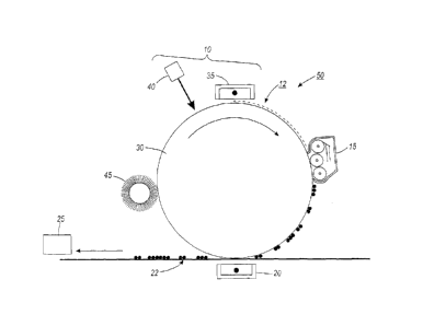
[0019] FIG. 1 illustrates a conventional xerographic image-forming
apparatus 5 in which the electrostatic latent image is formed via
photodischarge after scorotron charging. As seen, the conventional image-
forming apparatus 5 comprises an electrostatic imaging device 10 having a
charge retentive-surface 12 for receiving an electrostatic latent image
thereon,
a development component 15 for applying a developer material to the charge-
retentive surface 12 to develop the electrostatic latent image to form a
developed image on the charge-retentive surface 12, a transfer component 20
for transferring the developed image from the charge-retentive surface 12 to a
copy substrate 22, and a fusing component 25 for fusing the developed image
to the copy substrate 22.
[0020] The electrostatic imaging device comprises an imaging member
30, an electrostatic charging device 35 for charging the surface of the
electrostatic imaging member and an exposing device 40 for exposing the
surface of the electrostatic imaging member 30 to light. In FIG. 1, the charge
retentive surface 12 of the electrostatic imaging member 30 must be charged
and then discharged to form an electrostatic charge pattern, known as a latent
6
CA 02783033 2012-07-09
image, conforming to the original image. The latent image is developed by
contacting it with a finely divided electrostatically attractable powder known
as
toner. Toner is held on the image areas by the electrostatic charge on the
imaging member surface. The toner image may then be transferred to a
substrate or support member (e.g., paper) directly or through the use of an
intermediate transfer member 20, and the image affixed thereto to form a
permanent record of the image to be reproduced or printed. Subsequent to
development, excess toner left on the charge retentive surface is cleaned
from the surface 12 by, for example, a cleaning brush 45.
[0021] FIG. 2 illustrates a xerographic image-forming apparatus 50 in
accordance with the present embodiments. As seen, the image-forming
apparatus 50 of the present embodiments has similar components and
structure as the conventional image-forming apparatus except that the
exposing device 40 and the electrostatic charging device 35 in the
electrostatic imaging device 10 are positioned in reverse order as compared
to that found in the conventional image-forming apparatus 5. In such
embodiments, the latent image is formed during charging. Charge
acceptance is controlled by using a charge or hole transport molecule that has
variable charge acceptance dependent on light exposure and selectively pre-
exposing the imaging member to light before surface charging. Because the
charge is not accepted by the selectively exposed surface of the electrostatic
imaging member, an electrostatic image can be generated in a single
charging step. Thus, by using charge acceptance control rather than
convention photodischarge, the process is not limited by photodischarge time.
In these embodiments, the exposing device provides a light having an
intensity of from about 100ergs/cm2 to about 5000ergs/cm2, or from about
1000ergs/cm2 to about 3000ergs/cm2. In these embodiments, the exposing
device is selected from the group consisting of a laser raster output scanner
(ROS) and a light-emitting diode (LED) array. The electrostatic charger may
be selected from the group consisting of a corotron, scorotron and biased
charge roller.
[0022] In the present embodiments, the imaging member comprises a
substrate, a charge generation layer disposed on the substrate, and a charge
transport layer disposed on the charge generation layer, wherein the charge
7
CA 02783033 2012-07-09
transport layer comprises a charge transport molecule. In particular
embodiments, the charge transport molecule is N,N,N',N'-tetra(4-
methylpheny1)-(1,1'-bipheny1)-4,4'-diamine.
[0023] The charge transport layer may also include any suitable charge
transport component or activating compound useful as an additive dissolved
or molecularly dispersed in an electrically inactive polymeric material, such
as
a polycarbonate binder, to form a solid solution and thereby making this
material electrically active. "Dissolved" refers, for example, to forming a
solution in which the small molecule is dissolved in the polymer to form a
homogeneous phase; and molecularly dispersed in embodiments refers, for
example, to charge transporting molecules dispersed in the polymer, the small
molecules being dispersed in the polymer on a molecular scale. The charge
transport component may be added to a film forming polymeric material which
is otherwise incapable of supporting the injection of photogenerated holes
from the charge generation material and incapable of allowing the transport of
these holes through. This addition converts the electrically inactive
polymeric
material to a material capable of supporting the injection of photogenerated
holes from the charge generation layer and capable of allowing the transport
of these holes through the charge transport layer in order to discharge the
surface charge on the charge transport layer. The high mobility charge
transport component may comprise small molecules of an organic compound
which cooperate to transport charge between molecules and ultimately to the
surface of the charge transport layer.
[0024] Examples of charge transport components are aryl amines of
the following formulas/structures:
rry
0.-17-71\
and
x 1( K __
r
hN
R __________________________ X
8
CA 02783033 2012-07-09
wherein X is a suitable hydrocarbon like alkyl, alkoxy, aryl, and derivatives
thereof; a halogen, or mixtures thereof, and especially those substituents
selected from the group consisting of Cl and CH3; and molecules of the
following formulas
_
(/Q ______________________________________________ N.?
0 _________________________________________________________ X
and
=
N 0 0 N
x
X
wherein X, Y and Z are independently alkyl, alkoxy, aryl, a halogen, or
mixtures thereof, and wherein at least one of Y and Z are present.
[0025] Alkyl and alkoxy contain, for example, from 1 to about 25 carbon
atoms, and more specifically, from 1 to about 12 carbon atoms, such as
methyl, ethyl, propyl, butyl, pentyl, and the corresponding alkoxides. Aryl
can
contain from 6 to about 36 carbon atoms, such as phenyl, and the like.
Halogen includes chloride, bromide, iodide, and fluoride. Substituted alkyls,
alkoxys, and aryls can also be selected in embodiments.
[0026] One specific suitable charge transport material is N,N,NN-
tetra(4-methylpheny1)-(1,11-bipheny1)-4,4'-diamine, of the formula
9
CA 02783033 2014-06-03
H3C CH3
o 0
0 N
H3C CH3,
as disclosed in, for example, U.S. Patent Publication 2008/0102388, U.S.
Patent
Publication No. 2008/0299474, and European Patent Publication EP 1 918 779 Al.
[0027] Examples of specific aryl amines that can be selected for the charge
transport layer include, but not limited to, N,N'-diphenyl-N,N-bis(3-methyl
pheny1)-
1,11-bipheny1-4,4'-diamine (TPD); N,N,N',N'-tetra-p-toly1-1,1'-bipheny1-4,4'-
diamine
(TM-TPD); N,N'-diphenyl-N,N'-bis(alkylpheny1)-1,1-bipheny1-4,4'-diamine
wherein
alkyl is selected from the group consisting of methyl, ethyl, propyl, butyl,
hexyl, and
the like; N,N'-diphenyl-N,N'-bis(halopheny1)-1,1'-bipheny1-4,4'-diamine
wherein the
halo substituent is a chloro substituent; N,N'-bis(4-butylpheny1)-N,N'-di-p-
toly11p-
terpheny1]-4,4"-diamine; N,N'-bis(4-butylpheny1)-N,N'-di-m-toly14p-terpheny1]-
4,4"-
diamine; N,N1-bis(4-butylpheny1)-N,Ny-di-o-toly14p-terpheny1]-4,4"-diamine;
N,Nr-
bis(4-butylpheny1)-N,N'-bis-(4-isopropylpheny1)-[p-terpheny1]-4,4"-diamine;
N,N'-
bis(4-butylpheny1)-N,N'-bis-(2-ethy1-6-methylphenyl)-[p-terphenyl]-4,4"-
diamine; N,N'-
bis(4-butylpheny1)-N,N'-bis-(2,5-dimethylpheny1)-[p-terphenyl]-4,4'-diamine;
N,N'-
diphenyl-N,N'-bis(3-chlorophenyl)-[p-terpheny1]-4,4"-diamine, and the like.
Other
known charge transport layer molecules may be selected in embodiments,
reference
for example, U.S. Patents 4,921,773 and 4,464,450.
[0028] In the present embodiments, the charge transport molecule is
present
in the charge transport layer in an amount of from about 1% to about 60%, or
from
about 30% to about 50% percent weight of the total weight of the charge
transport
layer. The charge transport layer may have a thickness
CA 02783033 2014-06-03
of from about 2 microns to about 40 microns, or from about 20 microns to about
30
microns.
[0029] The present embodiments provide various advantages over the
conventional photoreceptor-based system. In particular, the formation of
electrostatic images is free from a post charging photo-induced discharge
period and
charge transport that are inherent with photoreceptor designs. This enables
high
speed operation and compact design due to simultaneous charging and latent
image
formation rather than imaging via photo-discharge.
[0030] All the exemplary embodiments encompassed herein include a method
of imaging which includes generating an electrostatic latent image on an
imaging
member, developing a latent image, and transferring the developed
electrostatic
image to a suitable substrate.
[0031] While the description above refers to particular embodiments, it
will be
understood that many modifications may be made without departing from the
scope
thereof. The accompanying claims are intended to cover such modifications as
would fall within the true scope of embodiments herein.
EXAMPLES
[0032] The development of the presently disclosed embodiments will
further
be demonstrated in the non-limiting examples below. They are, therefore in all
respects, to be considered as illustrative and not restrictive nor limited to
the
materials, conditions, process parameters, and the like recited herein. The
scope of
embodiments are being indicated by the appended claims rather than the
foregoing
description. All changes that come within the meaning of and range of
equivalency
of the claims are intended to be embraced therein. All proportions are by
weight
unless otherwise indicated. It will be apparent, however, that the present
embodiments can be practiced with many types of compositions and can have many
different uses in accordance with the disclosure above and as pointed out
hereinafter.
[0033] EXAMPLE 1
[0034] Prototype Fabrication
[0035] An electrical test fixture 55 was fabricated using an 84-mm drum
scanner
60, as shown in FIG. 3. The charging device 65 was a scorotron and
CA 02783033 2014-06-03
the exposing device 90 was an 630 nm LED line scan illuminator. The erase lamp
70 was a Xenon Lamp filtered to 780nm. The exposure system was placed before
the scorotron and the erase lamp was placed after electrostatic voltmeters
(ESV),
labeled ESV1 (75) and ESV2 (80). ESV3 (85) was located after the erase lamp.
The
test fixture 55 is capable of a maximum speed of 240 RPM which produces the
following timings (Table 1):
Table 1
Timings
High intensity exposure 0 ms
Scorotron 45 ms
ESV1 75 ms
ESV2 92 ms
Erase lamp 108 ms
ESV3 141 ms
[0036] Photoreceptor Fabrication
[0037] An imaging member was prepared in accordance with the following
procedure. A metallized MYLAR substrate was provided and a hydroxygallium
phthalocyanine (HOGaPc)/poly(bisphenol-Z carbonate) photogenerating layer was
machine coated over the substrate. A charge transport layer was prepared by
introducing into an amber glass bottle 50 weight percent of high quality
N,N,N'N'-
tetra(4-methylpheny1)-(1,1'-biphenyl)-4,41-diamine (Compound 1), and 50 weight
percent of a polymer binder, FPC-0170 polymer (available from Mitsubishi Gas
Chemical Co.). As disclosed in U.S. Patent Publication No. 2009/0162637, FPC-
0170 is a polycarbonate polymer based on 98 percent bisphenol A and 2 percent
bisphenol Z and has a measured molecular weight range of 60,000 to 70,000 (as
measured by auto capillary viscometer).
12
CA 02783033 2012-07-09
[0038] The resulting mixture was then dissolved in methylene chloride to
form a solution containing 15 percent by weight solids. This solution was
applied on the photogenerating layer to form a layer coating that upon drying
(at 120 C for 1 minute) had a thickness of 30 microns. The imaging member
was then mounted onto a 84-mm diameter bare aluminum drum and
grounded.
[0039] Testing Method
[0040] Using the above measurement system, the photoreceptor was
mounted and the exposure line scanner energy was set to 3.9 ma as
measured by a photodiode for the "on-state," as shown in FIG. 4, and 0 ma as
measured by photodiode for the "off-state," as shown in FIG. 5. This setting
provided 3000 erg/cm2 of 630nm light to the photoreceptor for the "on-state".
The speed of the drum was set to 240 RPM. Next, the charge acceptance (as
ESV1 and ESV2 in FIG. 3) was measured for both the on and off states.
[0041] Results
[0042] The off-state produces very high charge acceptance (about 450 V),
equivalent to the charged state in conventional discharge area development
(DAD) xerography (FIG. 4.). The on-state produces very low charge
acceptance (about 40 V), equivalent to the discharged state in conventional
DAD xerography (FIG. 5).
[0043] It will be appreciated that various of the above-disclosed and
other features and functions, or alternatives thereof, may be desirably
combined into many other different systems or applications. Various
presently unforeseen or unanticipated alternatives, modifications, variations
or
improvements therein may be subsequently made by those skilled in the art
which are also intended to be encompassed by the following claims.
13