Note: Descriptions are shown in the official language in which they were submitted.
CA 02783226 2012 06 06
WO 2011/084317 PCT/US2010/059400
- 1 -
PANELBOARD HAVING A PARALLEL FEEDER BARS DISTRIBUTION
FIELD OF THE INVENTION
[0001] The present invention relates generally to electrical equipment
and, more
particularly, to electrical enclosures having a parallel feeder bars
distribution.
BACKGROUND OF THE INVENTION
[0002] Electrical enclosures, such as, for example, load centers,
typically house
multiple circuit breakers and/or related electrical accessories. Load centers
typically include
one main feeder bar or busbar per phase of electricity. To accommodate single
and/or multi-
phase circuit breakers, most load centers include multiple stabs, where each
stab is
configured to connect two branch circuit breakers with one of the busbars.
This connection
inherently creates a thermal limitation because the heat contributed by the
two circuit
breakers for each stab has to be dissipated through a single dissipation path,
from the stab
itself to the main feeder busbar, which creates a localized temperature rise.
To combat these
temperature rises, busbars have been oversized to allow temperature rises to
remain lower
than maximum allowed levels per safety regulations. However, busbars are
typically made of
copper, which is an expensive metal, so increasing the size of the busbars
increases the costs
of manufacturing the load center.
[0003] Thus, a need exists for an improved apparatus. The present
invention is
directed to satisfying one or more of these needs and solving other problems.
SUMMARY OF THE INVENTION
[0004] The present disclosure is directed to providing a load center,
which can
also be known as a panelboard. The load center can be configured to accept
different makes,
models, sizes, and types of circuit breakers and related electrical
accessories. The load center
includes an outer housing for mounting the load center into a building, such
as a residential
house. The housing has various inputs/outputs to receive electrical wires. For
a load center
in a typical single family home, the housing is mounted between two studs in a
wall. The
housing receives one or more live electrical lines from an electrical utility
company. Each
live electrical line electrically couples with a respective pair of generally
parallel busbars.
The pairs of generally parallel busbars are insulated from the housing and are
rigidly
positioned within the housing. Each of the pairs of generally parallel busbars
supplies one
CA 02783226 2012 06 06
WO 2011/084317 PCT/US2010/059400
- 2 -
phase of electricity to circuit breakers and/or related electrical accessories
that are plugged
into the load center.
[0005] The present disclosure includes a first set or plurality of
stabs that is
connected between a first pair of generally parallel busbars such that each
one of the first set
of stabs forms a bridge between a first one of the first pair of generally
parallel busbars and a
second one of the first pair of generally parallel busbars. For a load center
configured to
distribute two or more phases of electricity, the present disclosure further
provides a second
pair of generally parallel busbars and a second set of stabs that is connected
between the
second pair of generally parallel busbars such that each one of the second set
of stabs forms a
bridge between a first one of the second pair of generally parallel busbars
and a second one of
the second pair of generally parallel busbars. For a load center configured to
distribute three
phases of electricity, the present disclosure further provides a third pair of
generally parallel
busbars and a third set of stabs that is connected between the third pair of
generally parallel
busbars such that each one of the third set of stabs forms a bridge between a
first one of the
third pair of generally parallel busbars and a second one of the third pair of
generally parallel
busbars. The first, the second, and the third pairs of generally parallel
busbars are arranged
within the housing such that the first, the second, and the third set of stabs
are staggered
along a central axis of the load center. Additionally, each of the first, the
second, and the
third set of stabs includes a circuit breaker connecting surface. The circuit
breaker
connecting surfaces of each of the first, the second, and the third set of
stabs can be coplanar.
Each of the stabs of the present disclosure provide a respective bidirectional
path for
dissipating heat to the two generally parallel busbars connected thereto. Such
bidirectional
heat dissipation allows for a reduction in the size of busbars, which can
result in material cost
savings.
[0006] According to some embodiments a load center includes a housing,
a first
busbar, a second busbar, and a set of stabs. The first busbar is positioned
within the housing
for distributing a first phase of electricity entering the load center. The
second busbar is
positioned within the housing for distributing the first phase of electricity.
The second busbar
is generally parallel to the first busbar and electrically connected thereto.
Each of the set of
stabs is electrically connected to the first busbar and the second busbar.
[0007] According to some embodiments, a load center includes a
housing, a first
pair of generally parallel busbars, a first set of stabs, a second pair of
generally parallel
CA 02783226 2014-06-09
- 3 -
busbars, a second set of stabs, and a first insulating layer. The first pair
of generally
parallel busbars is positioned within the housing for distributing a first
phase of electricity.
The first set of stabs is physically and electrically connected between the
first pair of
generally parallel busbars. The second pair of generally parallel busbars is
positioned
within the housing for distributing a second phase of electricity. The second
set of stabs is
physically and electrically connected between the second pair of generally
parallel
busbars. The first insulating layer is positioned between the first pair of
busbars and the
second pair of busbars to electrically insulate the first phase of electricity
from the second
phase of electricity. The first and the second pairs of busbars are arranged
within the
housing such that the first set of stabs and the second set of stabs are
staggered.
According to some embodiments, a load center includes a housing; a
first busbar, positioned within the housing, for distributing a first phase of
electricity
entering the load center; a second busbar, positioned within the housing and
physically
separated from the first busbar, for distributing the first phase of
electricity, the second
busbar being generally parallel to the first busbar and electrically connected
thereto; and a
plurality of stabs, each of the plurality of stabs being physically and
electrically connected
to the first busbar and the second busbar and each of the plurality of stabs
being
configured to physically and electrically connect with two circuit breakers
within the load
center.
According to some embodiments, a load center includes a housing; a
first pair of generally parallel busbars, positioned within the housing, for
distributing a
first phase of electricity, each of the first pair of busbars being physically
separated from
each other; a first plurality of stabs physically and electrically connected
between the first
pair of busbars; a second pair of generally parallel busbars, positioned
within the housing,
for distributing a second phase of electricity, each of the second pair of
busbars being
physically separated from each other; a second plurality of stabs physically
and
electrically connected between the second pair of busbars; a first insulating
layer
positioned between the first pair of busbars and the second pair of busbars to
electrically
insulate the first phase of electricity from the second phase of electricity,
wherein the first
and the second pairs of busbars are arranged within the housing such that the
first plurality
of stabs and the second plurality of stabs are staggered, and wherein each of
the first
plurality of stabs and each of the second plurality of stabs are configured to
be physically
CA 02783226 2014-06-09
- 3a -
and electrically coupled with corresponding electrical connectors of two
separate and
distinct circuit breakers.
[0008] The
foregoing and additional aspects and embodiments of the present
invention will be apparent to those of ordinary skill in the art in view of
the detailed
description of various embodiments and/or aspects, which is made with
reference to the
drawings, a brief description of which is provided next.
BRIEF DESCRIPTION OF THE DRAWINGS
[0009] The
foregoing and other advantages of the invention will become
apparent upon reading the following detailed description and upon reference to
the
drawings.
[0010] FIG. 1 is
a perspective view of a load center according to some aspects
of the present disclosure;
[0011] FIG. 2 is
a top view of the load center of FIG. 1 according to some
aspects of the present disclosure;
[0012] FIG. 3A is
a perspective view of three pairs of generally parallel
busbars and three sets of stabs from FIGS. 1 and 2 with a housing and all
insulating layers
removed according to some aspects of the present disclosure;
[0013] FIG. 3B is
a cross-sectional front view of the three pairs of generally
parallel busbars and the three sets of stabs from FIG. 3A;
[0014] FIG. 4A is
a partial perspective view of a first pair of generally parallel
busbars and a first set of stabs according to some aspects of the present
disclosure;
[0015] FIG. 4B is
the partial perspective view of FIG. 4A having a first
insulating layer overlaid thereon according to some aspects of the present
disclosure;
CA 02783226 2012 06 06
WO 2011/084317 PCT/US2010/059400
- 4 -
[0016]
FIG. 4C is the partial perspective view of FIG. 4B having a second pair of
generally parallel busbars and a second set of stabs overlaid thereon
according to some
aspects of the present disclosure;
[0017]
FIG. 4D is the partial perspective view of FIG. 4C having a second
insulating layer overlaid thereon according to some aspects of the present
disclosure;
[0018]
FIG. 4E is the partial perspective view of FIG. 4D having a third pair of
generally parallel busbars and a third set of stabs overlaid thereon according
to some aspects
of the present disclosure;
[0019]
FIG. 4F is a partial perspective view a load center including the
components of FIGS. 4A-4E having a third insulating layer overlaid thereon
according to
some aspects of the present disclosure; and
[0020]
FIG. 4G is a partial perspective view of the load center of FIG. 4F having
two multiphase circuit breakers coupled thereto.
DETAILED DESCRIPTION OF THE ILLUSTRATED EMBODIMENTS
[0021]
Although the invention will be described in connection with certain
aspects and/or embodiments, it will be understood that the invention is not
limited to those
particular aspects and/or embodiments. On the contrary, the invention is
intended to cover all
alternatives, modifications, and equivalent arrangements as may be included
within the spirit
and scope of the invention as defined by the appended claims.
[0022]
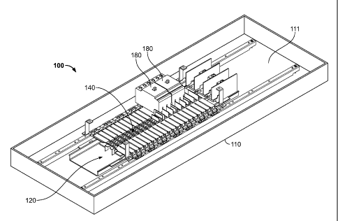
Referring to FIG. 1, an electrical enclosure or a load center 100 is shown
according to the present disclosure. The load center 100 includes a housing
110. The
housing 110 can be made of a variety of materials including metal, plastic,
fiberglass, and the
like. The housing 110 can include a hinged door (not shown) or other means of
sealing
and/or covering the contents of the load center 100. The housing 110 can also
include an
insulating base or pad 111 to cover all of or a portion of an interior surface
of the housing
110. The insulating base 111 is configured to electrically insulate the
contents of the load
center 100 from electrically conductive items outside the housing 110 (e.g.,
metal wall studs,
screws, wires, etc.).
[0023] The
load center 100 includes three pairs of generally parallel busbars 120
and three corresponding sets of stabs 140 (shown in more detail in FIG. 3A,
discussed
below), which are implemented to distribute three-phase power in the load
center. That is,
CA 02783226 2012 06 06
WO 2011/084317 PCT/US2010/059400
- 5 -
each pair of busbars and corresponding set of stabs are provided to supply a
separate and
distinct phase of electricity to one or more circuit breakers 180 coupled to
the load center
100. By generally parallel, it is meant that each pair of busbars 120 is
designed and installed
to be substantially parallel to one another, understanding that the practical
limitations of
mechanical and human imperfections can cause the busbars to be slightly
skewed. As shown
in FIG. 1, the circuit breakers 180 coupled with the load center 100 are three-
phase circuit
breakers; however, it is contemplated that the load center 100 can receive and
supply power
to single-phase circuit breakers, dual-phase circuit breakers, three-phase
circuit breakers, or a
combination thereof
[0024] While specific numbers of pairs of busbars 120 and
corresponding stabs
140 are described herein and shown in the Figures, it is contemplated that the
load center 100
can include any number of pairs of busbars 120 and corresponding stabs 140.
For example,
in some embodiments, the load center 100 is a single-phase load center that
includes only one
pair of busbars 120 and one corresponding set of stabs 140. For another
example, the load
center 100 is a dual-phase load center that includes two pairs of busbars 120
and two
corresponding sets of stabs 140. For yet another example, the load center 100
is a three-
phase load center that includes three pairs of busbars 120 and three
corresponding sets of
stabs 140.
[0025] Referring to FIG. 2, a top view of the load center 100 is
shown. As shown
in FIG. 3A, the pairs of busbars 120 are formed from any electrically
conducting material, as
is known in the art, such as copper. The pairs of busbars 120 are positioned
within the
housing 110 such that each of the pairs of busbars 120 are electrically
insulated from the
housing 100 and from each other. The busbars 120 can be positioned between and
held
rigidly in place by a first block 112 and a second block 114. The first and
the second blocks
112 and 114 are attached or coupled to the housing 110 and/or the insulating
base 111 such
that the first and the second blocks 112 and 114 aid in electrically
insulating the pairs of
busbars 120 from the housing 110. The first block 112 includes a first
terminal 112a, a
second terminal 112b, and a third terminal 112c. Each of the first, the
second, and the third
terminals 112a,b,c is configured to be electrically connected with a
respective one of the pairs
of busbars 120.
[0026] Referring to FIGS. 2 and 3A, a first pair of generally parallel
busbars 120a
is configured to be coupled with the first terminal 112a through a first
attachment member
CA 02783226 2012 06 06
WO 2011/084317 PCT/US2010/059400
- 6 -
121a. The first attachment member 121a can be integral with, or attached to,
one end of one
or both of the first pair of generally parallel busbars 120a. Similarly, a
second pair of
generally parallel busbars 120b is configured to be coupled with the second
terminal 112b
through a second attachment member 121b. The second attachment member 121b can
be
integral with, or attached to, one end of one or both of the second pair of
generally parallel
busbars 120b. Similarly, a third pair of generally parallel busbars 120c is
configured to be
coupled with the third terminal 112c through a third attachment member 121c.
The third
attachment member 121c can be integral with, or attached to, one end of one or
both of the
third pair of generally parallel busbars 120c.
[0027] Referring specifically to FIG. 2, the housing 110 includes one
or more
apertures positioned adjacent to the terminals 112a,b,c and configured to
receive electrical
supply lines 119a,b,c. The first, the second, and the third terminals 112a,b,c
include
respective attachment means, such as, for example, a lug, screw, or bolt to
aid in the electrical
coupling and physical attachment of the electrical supply wires 119a,b,c. The
electrical
supply wires 119a,b,c are electrically and physically coupled with the
respective terminals
112a,b,c via the screws or the like to supply distinct and separate phases of
electricity to the
first pair of busbars 120a, the second pair of busbars 120b, and the third
pair of busbars 120c,
respectively. For example, the first electrical supply wire 119a supplies a
first phase of
electricity to the first pair of generally parallel busbars 120a via the first
terminal 112a; the
second electrical supply wire 119b supplies a second phase of electricity to
the second pair of
generally parallel busbars 120b via the second terminal 112b; and the third
electrical supply
wire 119c supplies a third phase of electricity to the third pair of generally
parallel busbars
120c via the third terminal 112c.
[0028] Referring specifically to FIG. 3A, the three pairs of generally
parallel
busbars 120a,b,c and corresponding set of stabs 140a,b,c are shown with the
housing 110
removed and all insulating layers removed to illustrate a stacked and
staggered configuration
of the pairs of busbars 120a,b,c and the corresponding set of stabs 140a,b,c.
That is, the first,
the second, and the third pairs of generally parallel busbars 120a,b,c are
stacked relative to
each other such that at least a portion of each pair of busbars lies in a
different vertical plane.
Additionally, the first, the second, and the third pairs of generally parallel
busbars 120a,b,c
are staggered such that the first, the second, and the third pluralities of
stabs 140a,b,c,
respectively, alternate along a coinciding central axis as described below.
CA 02783226 2012 06 06
WO 2011/084317 PCT/US2010/059400
- 7 -
[0029] The first pair of generally parallel busbars 120a is shown on
the top of the
stack. The first pair of busbars 120a includes a first busbar 120a1 that is
parallel with and
coplanar with a second busbar 120a2. The first busbar 120a1 and the second
busbar 120a2 are
shown as resembling flat sheets, although it is contemplated that,
alternately, the first busbar
120a1 and/or the second busbar 120a2 can have an "L" configuration and/or a
"C"
configuration. The first busbar 120a1 and the second busbar 120a2 are
physically and
electrically connected by the first set of stabs 140a1_7. While FIG. 3A
illustrates seven stabs
140a, the first set of stabs 140a can include any number of stabs, such as,
for example, 1, 3, 5,
7, 10, 100, etc., to accommodate a variety of different numbers of circuit
breakers within the
load center 100. While the first set of stabs 140a is shown as having an open
trapezoidal
shape, it is contemplated that each one of the first set of stabs 140a can
have a "C" shape, a
substantially flat sheet shape, or an "L" shape.
[0030] The second pair of generally parallel busbars 120b is shown on
the bottom
of the stack. The second pair of busbars 120b includes a first busbar 120b1
that is parallel
with and at least partially coplanar with a second busbar 120b2. In other
words, major
corresponding surfaces 122b1, 122b2 (shown in FIG. 3B) of each of the second
pair of
busbars 120b share a common plane. The first busbar 120b1 and the second
busbar 120b2 are
shown as having an "L" configuration, although it is contemplated that in some
alternative
embodiments the first busbar 120b1 and/or the second busbar 120b2 can have a
flat sheet
configuration like the first pair of busbars 120a and/or a "C" configuration.
The first busbar
120b1 and the second busbar 120b2 are physically and electrically connected by
the second
set of stabs 140b1_7. While FIG. 3A illustrates seven stabs in the second set
of stabs 140b for
connecting up to 14 circuit breakers, it is contemplated that the second set
of stabs 140b can
include any number of stabs that corresponds with the number of stabs in the
first set of stabs
140a, such as, for example, 1, 3, 5, 7, 10, 100, etc. While the second set of
stabs 140b is
shown as having a "C" shape, it is contemplated that each one of the second
set of stabs 140b
can have a trapezoidal shape, a substantially flat sheet shape, or an "L"
shape.
[0031] The third pair of generally parallel busbars 120c is shown
between the first
and the second pairs of generally parallel busbars 120a,b in the stack. The
third pair of
busbars 120c includes a first busbar 120ci that is parallel with and at least
partially coplanar
with a second busbar 120c2. In other words, major corresponding surfaces
122ci, 122c2
(shown in FIG. 3B) of each of the third pair of busbars 120c share a common
plane. The first
CA 02783226 2012 06 06
WO 2011/084317 PCT/US2010/059400
- 8 -
busbar 120ci and the second busbar 120c2 are shown as having an "L"
configuration,
although it is contemplated that the first busbar 120ci and/or the second
busbar 120c2 can
alternately have a flat sheet configuration like the first pair of busbars
120a and/or a "C"
configuration. The first busbar 120ci and the second busbar 120c2 are
physically and
electrically connected by the third set of stabs 140c1_7. While FIG. 3A
illustrates seven stabs
in the third set of stabs 140c, it is contemplated that the third set of stabs
140c can include
any number of stabs that corresponds with the number of stabs in the first set
of stabs 140a,
such as, for example, 1, 3, 5, 7, 10, 100, etc. While the third set of stabs
140c is shown as
having a "C" shape, it is contemplated that each one of the third set of stabs
140c can have a
trapezoidal shape, a substantially flat sheet shape, or an "L" shape.
[0032] The first pair of generally parallel busbars 120a has a first
central axis
125a that is located equidistantly between the first busbar 120a1 and the
second busbar 120a2.
Similarly, the second pair of generally parallel busbars 120b has a second
central axis 125b
that is located equidistantly between the first busbar 120b1 and the second
busbar 120b2 and
the third pair of generally parallel busbars 120c has a third central axis
125c that is located
equidistantly between the first busbar 120ci and the second busbar 120c2.
According to some
embodiments, the first central axis 125a, the second central axis 125b, and
the third central
axis 125c, all coincide with each other or are one and the same. That is, the
first central axis
125a coincides with the second central axis 125b and the third central axis
125c.
[0033] Referring to FIG. 3B, a cross-sectional front view of the
stacked and
staggered configuration of busbar pairs 120a,b,c of FIG. 3A is shown. As shown
in FIG. 3B,
the first pair of busbars 120a is stacked above the third pair of busbars
120c, both of which
are stacked on top of the second pair of busbars 120b. As described herein in
reference to
FIGS. 4A-G, each of the pairs of busbars 120a,b,c is separated and
electrically insulated
using insulating layers (not shown in FIG. 3B) that are sandwiched between the
pairs of
busbars 120a,b,c.
[0034] Referring generally to FIGS. 4A-4G, the pairs of busbars 120
and the sets
of stabs 140 are described according to an implementation of the present
disclosure.
Referring specifically to FIG. 4A, a partial perspective view of the second
pair of busbars
120b and the second set of stabs 140b is shown. The first busbar 120b1 of the
second pair of
generally parallel busbars 120b has a substantially flat major surface 122b1
and opposing
edge surfaces 123b1, 123b2. Similarly, the second busbar 120b2 of the second
pair of
CA 02783226 2012 06 06
WO 2011/084317 PCT/US2010/059400
- 9 -
generally parallel busbars 120b has a substantially flat major surface 122b2
and opposing
edge surfaces 124b1, 124b2.
[0035] The
second pair of generally parallel busbars 120b is positioned within the
housing 110 such that the substantially flat major surface 122b1 of the first
busbar 120b1 is
coplanar with the substantially flat major surface 122b2 of the second busbar
120b2. As
described above, the second pair of generally parallel busbars 120b has a
second central axis
125b that is located equidistantly between the first busbar 120b1 and the
second busbar 120b2.
Additionally, the opposing edge surfaces 123b1 and 123b2 of the first busbar
120b1 and the
opposing edge surfaces 124b1 and 124b2 of the second busbar 120b2 are parallel
with the
second central axis 125b.
[0036] The
second set of stabs 140b is positioned along the second central axis
125b to physically and electrically connect the first busbar 120b1 with the
second busbar
120b2. That is, each one of the second set of stabs 140b physically and
electrically couples
the first busbar 120b1 with the second busbar 120b2. As shown in FIG. 4A, each
one of the
second set of stabs 140b, such as, for example, the second stab 140b2, is
coupled with the first
busbar 120b1 via a first screw 143b and the second busbar 120b2 via a second
screw 143b. It
is contemplated that each of the second set of stabs 140b can be coupled with
the first and/or
the second busbars 120b1, 120b2, via screw(s), nuts and bolts, welds, snap-fit
connection, or a
combination thereof.
[0037]
Each of the second set of stabs 140b has a circuit breaker connecting
surface 145b that is configured to be coupled with corresponding electrical
connectors (not
shown) of two separate and distinct circuit breakers. As shown, each of the
second set of
stabs 140b includes two apertures 14 lb. Each of the apertures 141b is
configured to receive a
screw, bolt, or the like to physically and/or electrically couple a circuit
breaker, as shown in,
for example, FIG. 4G, with the second pair of busbars 120b. The circuit
breaker connecting
surfaces 145b of each one of the second set of stabs 140b are coplanar with
one another.
That is, for example, the circuit breaker connecting surface 145b of the first
stab 140b1 is
coplanar with the circuit breaker connecting surface 145b of the second stab
140b2, the third
stab 140b3, the fourth stab 140b4, the fifth stab 140b5, etc. The coplanar
circuit breaker
connecting surfaces 145b of the second set of stabs 140b provide a uniform
platform for
coupling circuit breakers. As will be explained below, the first and the third
sets of stabs
140a,c also include circuit breaker connecting surfaces 145a,c that are
coplanar with the
CA 02783226 2012 06 06
WO 2011/084317 PCT/US2010/059400
- 10 -
circuit breaker connecting surfaces 145b of the second set of stabs 140b such
that multiphase
circuit breakers, such as, for example, the circuit breakers 180, shown in
FIG. 1, can be
physically and electrically connected with the first, the second, and the
third phases of
electricity entering the load center 100.
[0038] As described above, each of the second set of stabs 140b forms
a bridge
between the first busbar 120b1 and the second busbar 120b2 to (1) physically
and electrically
connect the first busbar 120b1 and the second busbar 120b2 and (2) provide a
circuit breaker
connecting surface 145b that is configured to be coupled with corresponding
electrical
connectors of two separate and distinct circuit breakers. In addition, each of
the second set of
stabs 140b forms a bridge between the first busbar 120b1 and the second busbar
120b2 to (3)
provide a bidirectional path for dissipating heat generated by electrical
current conducted
between the busbars and the attached circuit breakers from each one of the
second set of stabs
140b to the first busbar 120b1 and to the second busbar 120b2.
[0039] For example, as shown in FIG. 1, circuit breakers 180 can be
connected
with one or more of the second set of stabs 140b. During operation of the load
center 100 in,
for example, a residential house, electrical current passes through the
circuit breakers 180,
which creates heat in the circuit breakers 180. Heat is dissipated from the
circuit breakers
180 to the second pair of busbars 120b in a bidirectional manner via the
second set of stabs
140b. That is, heat can travel from each one of the second set of stabs 140b
in one of two
directions as each one of the second set of stabs 140b is physically and
electrically connected
to the first busbar 120b1 and to the second busbar 120b2. In other words, heat
can travel
from, for example, the second stab 140b2 in a first direction to the first
busbar 120b1 or in a
second direction to the second busbar 120b2.
[0040] Now referring to FIG. 4B, the second pair of generally parallel
busbars
120b and the second set of stabs 140b of FIG. 4A are shown having a second
insulating layer
150b overlaid thereon. Only a portion of the second insulating layer 150b is
shown to
illustrate how the second pair of busbars 120b extends beneath the second
insulating layer
150b. The second insulating layer 150b can be a single part or multiple parts.
For example,
the second insulating layer 150b can be broken into sections that electrically
insulate
respective portions of the second pair of busbars 120b. It is contemplated
that the second
insulating layer 150b is made of any electrically insulating material, such
as, for example,
plastic, rubber, etc.
CA 02783226 2012 06 06
WO 2011/084317 PCT/US2010/059400
- 11 -
[0041] The second insulating layer 150b includes an insulator base 15
lb, phase
barriers 153b, and apertures 155b. Each of the phase barriers 153b extends
perpendicularly
from the insulator base 15 lb to aid in electrically insulating the second
phase of electricity
entering the load center 100 through the second electrical supply line 119b
from the first
phase of electricity entering the load center 100 through the first electrical
supply line 119a
and from the third phase of electricity entering the load center 100 through
the third electrical
supply line 119c. The phase barriers 153b are configured to be received
between circuit
breakers and/or within respective slots in a multiphase circuit breaker, such
as, for example,
as shown in FIG. 1.
[0042] Each of the apertures 155b is positioned to allow access to a
respective
underlying stab. For example, the first aperture 155b1 is positioned to
provide access to the
first stab 140b1 of the second set of stabs 140b. Similarly, the second
aperture 155b2 is
positioned to provide access to the second stab 140b2, and the third aperture
155b3 is
positioned to provide access to the third stab 140b3. That is, the apertures
155b provide a
path for circuit breakers to physically and/or electrically couple with one of
the underlying
stabs, such as, for example, one of the second set of stabs 140b.
[0043] The insulator base 151b forms a substantially flat major
surface 152b that
at least partially rests on the substantially flat major surface 122b1 of the
first busbar 120b1 of
the second pair of busbars 120b and on the substantially flat major surface
122b2 of the
second busbar 120b2 of the second pair of busbars 120b, which provides a
portion of the
stacked and staggered configuration of busbars and stabs described herein.
[0044] Referring specifically to FIG. 4C, the second pair of generally
parallel
busbars 120b, the second set of stabs 140b, and the second insulating layer
150b of FIG. 4B
are shown having the third pair of generally parallel busbars 120c and the
third set of stabs
140c overlaid thereon. The first busbar 120c of the third pair of generally
parallel busbars
120c has a substantially flat major surface 122ci and opposing edge surfaces
123ci, 123c2.
Similarly, the second busbar 120c2 of the third pair of generally parallel
busbars 120c has a
substantially flat major surface 122c2 and opposing edge surfaces 124ci,
124c2.
[0045] The third pair of generally parallel busbars 120c is positioned
within the
housing 110 in the stacked and staggered configuration such that the
substantially flat major
surface 152b of the insulator base 151b is sandwiched between the
substantially flat major
surfaces 122b1 and 122b2 of the second pair of generally parallel busbars 120b
and the
CA 02783226 2012 06 06
WO 2011/084317 PCT/US2010/059400
- 12 -
substantially flat major surfaces 122ci and 122c2 of the third pair of
generally parallel busbars
120c. Additionally, the third pair of generally parallel busbars 120c is
positioned within the
housing 110 such that the substantially flat major surface 122ci of the first
busbar 120ci is
coplanar with the substantially flat major surface 122c2 of the second busbar
120c2. As
described above, the third pair of generally parallel busbars 120c has a third
central axis 125c
that is located equidistantly between the first busbar 120ci and the second
busbar 120c2.
Additionally, according to some embodiments, the opposing edge surfaces 123ci
and 123c2
of the first busbar 120ci and the opposing edge surfaces 124ci and 124c2 of
the second busbar
120c2 are parallel with the third central axis 125c.
[0046] The third set of stabs 140c is positioned along the third
central axis 125c to
physically and electrically connect the first busbar 120ci with the second
busbar 120c2. That
is, each one of the third set of stabs 140c physically and electrically
couples the first busbar
120ci with the second busbar 120c2. As shown in FIG. 4C, each one of the third
set of stabs
140c, such as, for example, the fifth stab 140c5, is coupled with the first
busbar 120ci via a
first screw 143c and the second busbar 120c2 via a second screw 143c. It is
contemplated
that each of the third set of stabs 140c can be coupled with the first and/or
the second busbars
120ci, 120c2, via screw(s), nuts and bolts, welds, snap-fit connection, or a
combination
thereof.
[0047] Each of the third set of stabs 140c has a circuit breaker
connecting surface
145c that is configured to be coupled with corresponding electrical connectors
of two
separate and distinct circuit breakers. As shown, each of the third set of
stabs 140c includes
two apertures 141c. Each of the apertures 141c is configured to receive a
screw, bolt, or the
like to physically and/or electrically couple a circuit breaker, as shown in,
for example, FIG.
4G, with the third pair of busbars 120c. The circuit breaker connecting
surfaces 145c of each
one of the third set of stabs 140c are coplanar. That is, for example, the
circuit breaker
connecting surface 145c of the first stab 140ci is coplanar with the circuit
breaker connecting
surface 145c of the second stab 140c2, the third stab 140c3, the fourth stab
140c4, the fifth
stab 140c5, etc. The coplanar circuit breaker connecting surfaces 145c of the
third set of stabs
140c provide a uniform platform for coupling circuit breakers as described
above in reference
to FIG. 4A.
[0048] As described above, each of the third set of stabs 140c forms a
bridge
between the first busbar 120ci and the second busbar 120c2 to (1) physically
and electrically
CA 02783226 2012 06 06
WO 2011/084317 PCT/US2010/059400
- 13 -
connect the first busbar 120ci and the second busbar 120c2 and (2) provide a
circuit breaker
connecting surface 145c that is configured to be coupled with corresponding
electrical
connectors of two separate and distinct circuit breakers. In addition, each of
the third set of
stabs 140c forms a bridge between the first busbar 120ci and the second busbar
120c2 to (3)
provide a bidirectional path for dissipating heat from each one of the third
set of stabs 140c to
the first busbar 120ci and the second busbar 120c2, in the same, or similar,
manner as
described above in reference to the second set of stabs and FIG. 4A.
[0049] As described above, the third set of stabs 140c is positioned
along the third
central axis 125c, which coincides with the second central axis, such that the
third set of
stabs 140c is staggered with respect to the second set of stabs 140b. That is,
the second set of
stabs 140b and the third set of stabs 140c are staggered such that respective
portions of the
second set of stabs 140b and respective portions of the third set of stabs
140c alternate along
the second central axis and the third central axis. The respective portions
are respective
circuit breaker connection surfaces 145b,c of the second and the third sets of
stabs 140b,c.
[0050] Now referring to FIG. 4D, the third pair of generally parallel
busbars 120c,
the third set of stabs 140c, the second insulating layer 150b, the second pair
of generally
parallel busbars 120b, and the second set of stabs 140b of FIG. 4C are shown
having a third
insulating layer 150c overlaid thereon. The third insulating layer 150c is the
same as, or
similar to, the second insulating layer 150b in that, the third insulating
layer 150c can be a
single part or multiple parts. It is contemplated that the third insulating
layer 150c is made of
any electrically insulating material, such as, for example, plastic, rubber,
etc.
[0051] The third insulating layer 150c includes an insulator base
151c, phase
barriers 153c, and apertures 155c. Each of the phase barriers 153c extends
perpendicularly
from the insulator base 151c to aid in electrically insulating the second
phase of electricity
entering the load center 100 through the second electrical supply line 119b
from the first
phase of electricity entering the load center 100 through the first electrical
supply line 119a
and from the third phase of electricity entering the load center 100 through
the third electrical
supply line 119c in the same or similar manner as described above in reference
to the phase
barriers 153b and FIG. 4B. Alternately, the third insulating layer 150c does
not include phase
barriers, and the phase barriers 153b of the second insulting layer 150b
provide sufficient
electrical insulation between phases.
CA 02783226 2012 06 06
WO 2011/084317 PCT/US2010/059400
- 14 -
[0052] Each of the apertures 155c is positioned to allow access to a
respective
underlying stab. For example, the first aperture 155ci is positioned to
provide access to the
first stab 140b1 of the second set of stabs 140b. Similarly, the second
aperture 155c2 is
positioned to provide access to the first stab 140ci of the third set of stabs
140c. That is, the
apertures 155c provide a path for circuit breakers to physically and/or
electrically couple with
one of the underlying stabs, such as, for example, one of the second and/or
the third sets of
stabs 140b,c.
[0053] The insulator base 151c forms a substantially flat major
surface 152c that
at least partially rests on the substantially flat major surface 122ci of the
first busbar 120c of
the third pair of busbars 120c and on the substantially flat major surface
122c2 of the second
busbar 120c2 of the third pair of busbars 120c, which provides a portion of
the stacked and
staggered configuration of busbars and stabs described herein.
[0054] Referring specifically to FIG. 4E, the third insulating layer
150c, the third
pair of generally parallel busbars 120c, the third set of stabs 140c, the
second insulating layer
150b, the second pair of generally parallel busbars 120b, and the second set
of stabs 140b of
FIG. 4D are shown having the first pair of generally parallel busbars 120a and
the first set of
stabs 140a overlaid thereon. The first busbar 120a1 of the first pair of
generally parallel
busbars 120a has a substantially flat major surface 122a1 and opposing edge
surfaces 123a1,
123a2. Similarly, the second busbar 120a2 of the first pair of generally
parallel busbars 120a
has a substantially flat major surface 122a2 and opposing edge surfaces 124a1,
124a2.
[0055] The first pair of generally parallel busbars 120a is positioned
within the
housing 110 in the stacked and staggered configuration such that the
substantially flat major
surface 152c of the insulator base 151c is sandwiched between the
substantially flat major
surfaces 122ci and 122c2 of the third pair of generally parallel busbars 120c
and the
substantially flat major surfaces 122a1 and 122a2 of the first pair of
generally parallel busbars
120a. Additionally, the first pair of generally parallel busbars 120a is
positioned within the
housing 110 such that the substantially flat major surface 122a1 of the first
busbar 120a1 is
coplanar with the substantially flat major surface 122a2 of the second busbar
120a2. As
described above, the first pair of generally parallel busbars 120a has a first
central axis 125a
that is located equidistantly between the first busbar 120a1 and the second
busbar 120a2.
Additionally, the opposing edge surfaces 123a1 and 123a2 of the first busbar
120a1 and the
CA 02783226 2012 06 06
WO 2011/084317 PCT/US2010/059400
- 15 -
opposing edge surfaces 124a1 and 124a2 of the second busbar 120a2 are parallel
with the first
central axis 125a.
[0056] The first set of stabs 140a is positioned along the first
central axis 125a to
physically and electrically connect the first busbar 120a1 with the second
busbar 120a2. That
is, each one of the first set of stabs 140a physically and electrically
couples the first busbar
120a1 with the second busbar 120a2. As shown in FIG. 4E, each one of the first
set of stabs
140a, such as, for example, the third stab 140a3, is coupled with the first
busbar 120a1 via a
first screw 143a and the second busbar 120a2 via a second screw 143a. It is
contemplated
that each of the first set of stabs 140a can be coupled with the first and/or
the second busbars
120a1, 120a2, via screw(s), nuts and bolts, welds, snap-fit connection, or a
combination
thereof.
[0057] Each of the first set of stabs 140a has a circuit breaker
connecting surface
145a that is configured to be coupled with corresponding electrical connectors
of two
separate and distinct circuit breakers. As shown, each of the first set of
stabs 140a includes
two apertures 141a. Each of the apertures 141a is configured to receive a
screw, bolt, or the
like to physically and/or electrically couple a circuit breaker, as shown in,
for example, FIG.
4G, with the first pair of busbars 120a. The circuit breaker connecting
surfaces 145a of each
one of the first set of stabs 140a are coplanar. That is, for example, the
circuit breaker
connecting surface 145a of the first stab 140a1 is coplanar with the circuit
breaker connecting
surface 145a of the second stab 140a2, the third stab 140a3, the fourth stab
140a4, the fifth
stab 140a5, etc. The coplanar circuit breaker connecting surfaces 145a of the
first set of stabs
140a provide a uniform platform for coupling circuit breakers as described
above in reference
to FIG. 4A.
[0058] As described above, each of the first set of stabs 140a forms a
bridge
between the first busbar 120a1 and the second busbar 120a2 to (1) physically
and electrically
connect the first busbar 120a1 and the second busbar 120a2 and (2) provide a
circuit breaker
connecting surface 145a that is configured to be coupled with corresponding
electrical
connectors of two separate and distinct circuit breakers. In addition, each of
the first set of
stabs 140a forms a bridge between the first busbar 120a1 and the second busbar
120a2 to (3)
provide a bidirectional path for dissipating heat from each one of the first
set of stabs 140a to
the first busbar 120a1 and the second busbar 120a2, in the same, or similar
manner as
described herein in reference to the second set of stabs and FIG. 4A.
CA 02783226 2012 06 06
WO 2011/084317 PCT/US2010/059400
- 16 -
[0059] As described above, the first set of stabs 140a is positioned
along the first
central axis 125a, which coincides with the second, and the third central
axes, such that the
first set of stabs 140a are staggered with respect to the second set of stabs
140b and with
respect to the third set of stabs 140c. That is, the first set of stabs 140a,
the second set of
stabs 140b, and the third set of stabs 140c are staggered such that respective
portions of the
first set of stabs 140a, respective portions of the second set of stabs 140b,
and respective
portions of the third set of stabs 140c alternate along the first, the second,
and the third
central axes.
[0060] Now referring to FIG. 4F, a partial perspective view of the
load center 100
is shown. The load center 100 is shown as having the first pair of generally
parallel busbars
120a, the first set of stabs 140a, the third insulating layer 150c, the third
pair of generally
parallel busbars 120c, the third set of stabs 140c, the second insulating
layer 150b, the second
pair of generally parallel busbars 120b, and the second set of stabs 140b of
FIG. 4E with a
first insulating layer 150a overlaid thereon. The first insulating layer 150a
is similar to the
second insulating layer 150b and the third insulating layer 150c in that, the
first insulating
layer 150a can be a single part or multiple parts. It is contemplated that the
first insulating
layer 150a is made of any electrically insulating material, such as, for
example, plastic,
rubber, etc.
[0061] The first insulating layer 150a includes an insulator base 151a
and
apertures 155a. Each of the apertures 155a is positioned to allow access to a
respective
underlying stab. For example, the first aperture 155a1 is positioned to
provide access to the
first stab 140a1 of the first set of stabs 140a. Similarly, the second
aperture 155a2 is
positioned to provide access to the first stab 140b1 of the second set of
stabs 140b and the
third aperture 155a3 is positioned to provide access to the first stab 140ci
of the third set of
stabs 140c. That is, the apertures 155a provide a path for circuit breakers to
physically and/or
electrically couple with one of the underlying stabs, such as, for example,
one of the first, the
second, and/or the third sets of stabs 140a,b,c. According to some alternative
embodiments,
the stabs protrude through the apertures 155a.
[0062] The first insulating layer 150a does not include phase
barriers. The phase
barriers 153b, 153c of the second and the third insulating layers 150b,c
protrude through the
apertures 155a. The first insulating layer 150a can further include phase
barriers the same as,
or similar to, the phase barriers 153b, 153c described above in reference to
FIGS. 4B and 4D.
CA 02783226 2012 06 06
WO 2011/084317 PCT/US2010/059400
- 17 -
[0063] The insulator base 151a forms a substantially flat major
surface 152a that
at least partially rests on the substantially flat major surface 122a1 of the
first busbar 120a1 of
the first set of busbars 120a and on the substantially flat major surface
122a2 of the second
busbar 120a2 of the first set of busbars 120a, which provides a portion of the
stacked and
staggered configuration of busbars and stabs described herein.
[0064] Now referring to FIG. 4G, the partial perspective view of the
load center
100 of FIG. 4F is shown having two multi-phase circuit breakers 180a,b coupled
thereto.
Each of the circuit breakers 180a,b includes a first electrical connector
182a, a second
electrical connector 182b, and a third electrical connector 182c. The
electrical connectors
182a,b,c of each circuit breaker 180a,b correspond with respective stabs for
receiving
respective phases of electricity. For example, the first electrical connector
182a of the first
circuit breakers 180a corresponds with the second stab 140a2 of the first set
of stabs 140a to
receive the first phase of electricity; the second electrical connector 182b
of the first circuit
breakers 180a corresponds with the second stab 140b2 of the second set of
stabs 140b to
receive the second phase of electricity; and the third electrical connector
182c of the first
circuit breakers 180a corresponds with the second stab 140c2 of the third set
of stabs 140c to
receive the third phase of electricity. The first, the second, and the third
electrical connectors
182a,b,c are positioned to be fixedly connected with the corresponding stabs
via, for
example, a screw.
[0065] The first, the second, and the third electrical connectors
182a,b,c can be
configured to snap-on corresponding stabs such that each of the first, the
second, and the
third electrical connectors 182a,b,c is physically and electrically connected
to a respective
stab.
[0066] It is contemplated that bidirectional heat dissipation, as
described herein,
allows for a reduction in a size or thickness of the pairs of busbars 120 as
compared with
prior art load centers that have stabs with unidirectional heat dissipation
that are physically
and/or electrically coupled with only one busbar for each phase of electricity
being
distributed in the load center. A reduction in a thickness of the busbars
results in a reduction
of copper needed to produce a load center, such as the load center 100. It is
contemplated
that bidirectional heat dissipation, as described herein, also provides load
centers that have an
increased efficiency as compared with prior art load centers that have stabs
with
CA 02783226 2012 06 06
WO 2011/084317 PCT/US2010/059400
- 18 -
unidirectional heat dissipation that are physically and/or electrically
coupled with only one
busbar for each phase of electricity being distributed in the load center.
[0067] A load center having bidirectional heat dissipation, as
described herein,
can be made with 20 percent to 35 percent less copper compared to prior art
load centers that
have stabs with unidirectional heat dissipation that are physically and/or
electrically coupled
with only one busbar for each phase of electricity being distributed in a load
center. A load
center having bidirectional heat dissipation, as described herein, can be made
with 25 percent
to 30 percent less copper compared to prior art load centers that have stabs
with
unidirectional heat dissipation that are physically and/or electrically
coupled with only one
busbar for each phase of electricity being distributed in a load center.
[0068] For example, a three-phase, low-amperage (e.g., 250 Amps) prior
art load
center having three busbars that are each 0.187 inches thick by 1.5 inches
wide and fifteen
stabs that are 0.187 inches thick by 0.5 inches wide, requires a total of
about 2.69 kilograms
of copper to produce such a load center. However, a three-phase, low-amperage
(e.g., 250
Amps) load center according to aspects of the present disclosure having three
pairs of
busbars, where each one of the busbars in each pair of busbars is 0.062 inches
thick by 1.5
inches wide and fifteen stabs that are 0.125 inches thick by 0.5 inches wide,
requires a total of
about 1.97 kilograms of copper to produce such a load center. That is, a three-
phase, low-
amperage (e.g., 250 Amps) load center according to aspects of the present
disclosure can be
produced with about 0.72 kilograms (26.7%) less of copper than a comparable
prior art load
center have the same circuit breaker capacity.
[0069] A load center according to the aspects of the present
disclosure having
bidirectional heat dissipation, as described herein, can be made with less
copper and be more
efficient (e.g., lose less heat) compared to prior art load centers that have
stabs with
unidirectional heat dissipation that are physically and/or electrically
coupled with only one
busbar for each phase of electricity being distributed in a load center.
[0070] Instead of including the apertures 141a,b,c, each one of the
first, the
second, and the third sets of stabs 140a,b,c can be configured to physically
and electrically
connect with one or more circuit breakers via a weld connection or a snap-fit
connection. For
a snap-fit connection, the circuit breakers include one or more jaw members
configured to
clamp or snap onto a portion of the circuit breaker connecting surface
145a,b,c.
CA 02783226 2014-06-09
,
- 19 -
[0071]
The scope of the claims should not be limited by the preferred
embodiments set forth in the examples, but should be given the broadest
interpretation consistent
with the description as a whole.