Note: Descriptions are shown in the official language in which they were submitted.
CA 02784125 2016-07-15
=
. I
ADDRESSABLE NODE UNIT AND METHOD FOR ADDRESSING
BACKGROUND
The invention relates to an addressable node unit. Such a node unit has, for
example,
become known from WO 2009/065236, which should be considered to be disclosed
here
by reference. Node units of this kind serve either as sensors (i.e. they
contain it) to moni-
tor exactly the occurrence of an event and the location of this event, wherein
generally a
plurality of such node units are arranged at distances from one another for
this purpose
along a cable or bus. However, it may also the question of a case, where the
respective
node unit carries out a control at a certain place, for example opening a
valve for spraying
fire fighting water, or it actuates a room partition, e.g. a fire protection
curtain, thus in each
case serving as an actor (this term hereafter shall be used, in general, for
such actua-
tions).
In the above prior art, nothing is disclosed regarding the manner of
addressing. However,
mainly two addressing systems are used up to now: Either an, e.g. binary,
address is as-
sociated to each node unit, which is called with a corresponding, e.g. binary,
signal by a
controller, such as a microprocessor, a computer or the like. A simplified
approach pro-
vides an addressing signal, the amplitude of which changes by line resistance
losses in
such a way that the amplitude itself can be used for addressing.
While the first mentioned addressing system is somewhat sumptuous, the second
one
cannot be employed without additional measures for branched lines and is,
moreover, not
adapted to transmit the address in a digital way.
Therefore, the invention is based on the object to provide a node unit adapted
to obtain a
digital address signal, wherein addressing should suitably be simplified, but
above all it
should be ensured, that the respective evaluating circuit is supplied
sufficiently with cur-
rent even in non-operating state.
SUMMARY
The switch actuated by the address signal, which can be totally simple and
does not need
an address code, ensures that the address signal initially reaches the
respective first node
unit in a row of such units, but passes then, at the next time, the address
signal to the next
node unit. At this moment, however, the first node unit, without additional
measures,
CA 02784125 2016-07-15
2
would be cut off the current supplying line. To ensure a minimum supply,
nevertheless,
the at least one current storage is provided.
This current storage, in principle, could be an accumulator or a chargeable
battery, but as
preferred is formed by at least one capacity, preferably by at least one
condenser. If a
difference is made here between a capacity and a condenser, the first term
should be
understood in general to encompass everything adapted to build-up a capacity
large
enough to provide the required current. This may be, for example, also an
accumulator
circuit (a chargeable battery).
In order to ensure that the stored current suffices really for the supply of
the evaluating
circuit during the period up to the next addressing of itself, the node unit
comprises advan-
tageously a switch over unit between the lines and the evaluating circuit, by
which current
consumption of the evaluating circuit may be reduced after opening of the
switch actuable
by the address signal.
According to another aspect of the invention a method for addressing one of at
least two
node units explained above is developed in such a way, that a first signal is
emitted for
addressing by a controller which reaches the first node unit, in which the
first signal is
supplied to the evaluating circuit, while passing this first signal to the
second node unit is
interrupted, after which the controller emits a second signal, different from
the first one, by
which the connection to the next node unit is established, but at the same
time or before-
hand the address signal path to the evaluating circuit of the first node unit
is interrupted,
so that the addressing first signal of the controller addresses now the second
node unit,
and that finally the connection between the controller and the evaluating
circuit of the first
node unit is reestablished finally for next addressing. With this method, in
comparison with
the prior art, outstandingly fast addressing is possible.
In accordance with one aspect of the present invention, there is provided an
addressable
node unit (30) comprising: a first and a second connection (15a, 15b, 16) for
at least a first
and a second line (17, 18a, 18b), through which the node unit (30) is
addressable, said
connections being connected to an evaluating circuit (14) useable to evaluate
an address-
ing signal, wherein a first switch (2a, 2b) is associated with the first
connection (15a, 15b,
16) and a second switch (2a, 2b) is associated with the second connection
(15a, 15b, 16),
wherein the first and the second switch (2a, 2b) are arranged so as to
establish, in a
closed state thereof, an electrical connection between the first and the
second connec-
tions (15a, 15b, 16), the switches (2a, 2b) being by-passed by respective
diodes with a
CA 02784125 2016-07-15
3
cathode (K) in common between the at least first and second lines (17, 18a,
18b) so that a
signal flow is possible in two directions; and at least one current source (4,
22), supply
able with current through at least one of the at least first and second lines
(17, 18a, 18b),
wherein a further switch (25) is connected to the cathode (K), in common with
the two
diodes, between the evaluating circuit (14) and a corresponding one of the
first and sec-
ond connections (15a, 15b), the further switch (25) being opened after
addressing so that
current supply to the evaluating circuit (14) is ensured, after addressing, by
the at least
one current source (4, 22), and data thereafter is exchangeable between the
evaluating
circuit (14) and the node unit (30).
In accordance with another aspect of the present invention, there is provided
a method for
addressing at least two node units (80-1 to 80-8, 81) via at least one
controller (70a, 70b),
the method comprising: emitting a first addressing signal (U1), via the at
least one control-
ler (70a), to a first node unit (80-1) of the at least two node units (80-1 to
80-8, 81), the
first addressing signal being delivered to an evaluating circuit (14)
connected to the first
node unit (80-1); interrupting passage of the first addressing signal (UI) to
a second node
unit (80-2) of the at least two node units (80-1 to 80-8, 81); emitting, via
the controller
(70a), a second addressing signal (U2) which is different from the first
addressing signal,
subsequent to the interrupting, by which connection is made to a respective
next node unit
(80-2) of the at least two node units (80-1 to 80-8, 81), the interrupting of
passage of the
first addressing signal to the evaluating circuit (14) connected to the first
node unit (80-1)
being achieved via a switch, opened after addressing such that the first
addressing signal
of the controller (70a) subsequently addresses the second node unit (80-2),
connection
between the controller and the evaluating circuit (14) connected to the first
node unit (80-
1) being re-establishable for subsequent addressing via a reset signal; and
interrupting
addressing of the respective next node unit, via a further switch connected to
cathodes (K)
in common with two diodes between the evaluating circuit (14) and
corresponding line
connections.
Further details of the invention will become apparent by the following
description of a pre-
ferred embodiment schematically shown in the drawing. There is shown in:
BRIEF DESCRIPTION OF THE DRAWINGS
Fig. 1 an embodiment of a node unit according to the invention;
CA 02784125 2016-07-15
' 3a
Fig. 2a the voltage (U) and current diagrams of the signals going over the
lines 17, 18 of
Fig. 1;
Fig. 2b the signal shapes at individual components of the circuit of Fig. 1;
Fig. 3 several node units being in series in a two wired line and being
addressed one
after the other by at least one controller;
Fig. 4 a variant to Fig. 1 in the particular application as an actor; and
Fig. 5 a preferred circuit diagram for a controller;
Fig. 6 variants of the embodiments of the switches; and
Fig. 7 an embodiment of the invention comprising double switches and current
storages.
DETAILED DESCRIPTION
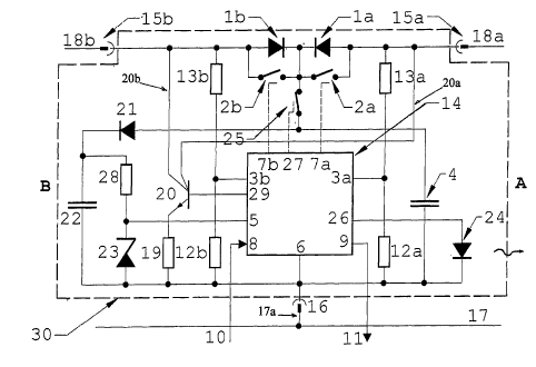
In Fig. 1, signal lines or connections 18a, 18b, or at least the signal line
18b of them, are
connected to a controller not shown (70a or 70b in Fig. 3, e.g. of the type of
LUMINARY
MICRO of the company of Texas Instruments). These lines 18a, 18b correspond to
the
respective side A or B of this sensor circuit or node unit 30. The circuit 30,
as may be
seen, is preferably removably connected to the connections 18a, 18b as well as
to a
negative signal line 17 via plug connections 15a, 15b and 16, as is explained
in detail in a
patent application simultaneously filed by the same applicant. It will be
understood, that
the function of the lines 17, 18a, 18b may, of course, be reversed, i.e. that
the line 17 has
positive voltage and the lines 18a, 18b the negative one. It will also be
understood that the
lines 17, 18 are suitably shielded. In this context one refers also to the
patent application
simultaneously filed by the same applicant.
In some embodiments, it may be advantageous, if the lines 18a, 18b are only
connected
via plug connections, while the output 6 is directly connected to the negative
line 17, for
example being soldered, because in this way possible tensile stress in
longitudinal direc-
tion has no effect to positioning of the node unit. Of course, the invention
is not limited to
plug connections, and plug connections 15a, 15b may rather be omitted. But
even with the
CA 02784125 2016-07-15
' 3b
arrangement of a plug connection 16, it is advantageous, if it is via a branch
line 17a, as
shown, so that the line 17 is uninterrupted, thus being able to absorb tensile
stress.
The line 18a may either be connected to another controller (70b in Fig. 3) or
in a circuit to
the same controller (70a in Fig. 3) so that this latter query measuring data
via one or the
other line. This corresponds about to an operation as described in WO
2009/065236. Al-
ternatively, the circuit 30, via connection 18a, is connected to a further (or
different) sen-
sor and/or actor circuit, and the controller addresses these circuits one
after the other to
obtain their measuring data, as it has been done already up to now.
CA 02784125 2012-06-12
4
The connections 18a, 18b represent here a bus and, for example, carry a
positive signal
in relationship with the signal of the negative line 17. The respective signal
is, thus,
sensed between these lines 17 and 18a, 18b. Addressing is done via a
changeover switch
device la, 1 b, 2a, 2b and 25 which, with opened switches 2a, 2b and closed
switch 25,
carries a signal only from the controller (e.g. 70a in Fig. 3) via the diode
lb, open in this
direction (diode 1 a blocks), and through the closed switch 25 to an
evaluating device 14.
This evaluating device delivers output signals, corresponding to its
measurements, via
outputs 26 and/or 29, after which the switches 2a, 2b are closed, but switch
25 is opened,
preferably on command of the controller, but optionally by a time circuit
within the evaluat-
ing device 14, so that the next enquiry signal of the controller arrives from
connection 18b,
via switches 2a, 2b, at connection 18a and from there at the next node unit to
be dialed,
having, in principle, the same changeover switch device 1 a, 1 b, 2a, 2b and
25, so that an
immense number of such modules 30 (in Fig. 3 designated 80-1 to 80-8) are
connected in
series and are able to be addressed in a simple manner. In practice, the
switches 2a, 2b,
will be electronic switches, such as transistors, particularly FET transistors
or MOS-
FETs.
Furthermore, switches, in the sense of the invention, shall be meant to be
electrical corn-
20 ponents, in general, which block in at least one direction, and may be
opened by signals.
For a more detailed description of these signals and components an their
control, it is re-
ferred to Figs. 6 and 7.
The node units 80-1 to 80-8 may be formed uniformly and, preferably, like the
node unit
25 30 shown in Fig. 1, or they are each different, for example so that an
infrared (heat) sen-
sor follows a photo-electric presence sensor. Because the controller is able
to determine
by addressing, which node unit it is facing and how the signal, coming from
it, has to be
judged or to be treated.
Changing over the switches 2a, 2b and 25 could, in principle, be effected
under time con-
trol, from receipt of an addressing order from the controller on, by a clock
generator of the
circuit 14 or by a program contained in the circuit 14, but it is preferred,
if changeover is
made by the controller and a signal delivered from it, as will be discussed
below with ref-
erence to Fig. 2a. If such a changeover signal appears, the switches 2a, 2b
are corres-
pondingly controlled via control outputs 7a, 7b, and switch 25 via a control
output 27. For
sensing, whether such a changeover signal from the respective controller is
present, vol-
tage dividers 12a, 13a and 12b, 13b are provided, which sense the voltage
existing be-
CA 02784125 2012-06-12
tween the lines 17 and 18. These voltage dividers, thus, contact permanently
the lines
18a, 18b, separated from one another by the diodes la, lb, so that they
receive voltage
signals even when switches 2a, 2b are closed and switch 25 is opened, in order
to enable
addressing the respective next node unit. By the presence of two voltage
sensors 12a,
5 13a and 12b, 13b, the voltages in the lines 18a and 18b can be sensed at
both sides A
and B independently from one another, and in dependence on the direction from
which an
address signal comes, as will be discussed later with reference to Fig. 2a,
the sensor sig-
nal processed by the evaluating circuit 14 will be sent, as far as two
directions are really
provided, for example to reach different controllers 70a, 70b (Fig. 3), to
which, however,
the present invention is not limited, since it could work also with signal
transmission in one
direction only. In this case, changeover device 1a, 1 b, 2a, 2b, and 25 is, of
course, simpli-
fied. The evaluation circuit is absolutely able to recognize, where (side A or
B) an address
or control signal is present and where not, and is able to send the processed
sensor sig-
nals correspondingly in the appropriate direction. A favorable solution, which
does without
additional changeover switches, will be discussed later with reference to
modulator tran-
sistor 20.
If the output 26 is utilized, it drives a diode circuit 24 (only one diode is
represented), so
that it releases, for example as an actor, an operation, as will be described
in detail with
reference to Fig. 4. However, it would also be possible, to provide here a
driver output for
a display to make the measurement visible to the exterior. The related
measurement sig-
nal from a sensor element (not shown), via an inlet line 10, reaches the inlet
8 of the eva-
luating circuit 14, whereas a further signal output 9 is connected to an
output line 11.
These lines 10, 11 may be a positive and a negative line each being connected
to the
sensor element 10a. The light emitting diode 24, for example, may emit in the
infrared
range. It is favorable, if the coating of the lines 17, 18 is transparent or
light transmissive
so that in the case of a failure and after switching the diode 24 on, the
place is optically
easy to determine in the case of an inspection by a custodian. Susceptibility
is particularly
enhanced, if the evaluating circuit 14 activates the diode 24 intermittently,
so that it emits
blinker light (function of an astable multivibrator within the circuit 14).
Of course, other light sources or actor circuits, for example using a relay,
are also con-
ceivable, but the use of a diode is structurally more favorable. To wit, the
diode is able to
emit also modulated signals, and by a corresponding circuitry of the
evaluating circuit 14 it
could be used to emit sensor data through a light-electric transducer or via
an optical con-
ductor, such as a fiber optical waveguide, receiving its light signals. In
such a case, the
diode could emit a pulse frequency and/or pulse width modulated light beam,
wherein the
CA 02784125 2012-06-12
6
diode is either placed at the surface of the circuit 30 or in a light
transmissive casing or by
connecting it from the interior via a light guide to outside. The light beam
of the diode 24 is
preferably in the infrared range.
The sensor connected to the line 10 may be of any kind, such as a temperature
sensor of
known type, if the temperature should be monitored, or a metal sensor
(capacitive, induc-
tive or the like), to determine the occupancy of a parking house with cars, a
humidity sen-
sor to determine a leakage, and so on. Instead of a sensor placed outside,
which delivers
its signals over the lines 10, 11 to the evaluating circuit, the sensor may
also be incorpo-
rated into the circuit 14.
A particular form of a sensor element may be the form of a sensor for
measuring distor-
tions of the geomagnetic field, for example to determine undesirable
deformations of a
pipeline. In this connection, the node units are mounted alongside a
ferromagnetic object,
for example a pipeline, where relative movements between the metered value
transducer
and the ferromagnetic object cause changes of the geomagnetic field at the
place of the
node unit. In this arrangement, the metered value transducer and the
ferromagnetic object
are mechanically fixed independently from one another. Such sensors, however,
may also
be used for other pipes, such as water pipes or gas pipes, sewage networks and
also for
managing parking houses.
It should be noted, that the signal lines 10, 11, if provided and if the
sensor here not
shown is not incorporated into the circuit 14, are, of course, insulated from
the potential of
the lines. This may be done in a manner that the signal lines are formed as
optical con-
ductors, whose transmitted light is controlled from a LED (similar to LED 24)
controlled by
the sensor signal, and at its output, this light is supplied in an analogous
way, i.e. via a
photoelectric transducer, as a voltage to the positive and negative input 8
and 9.
A modulator connection 29 serves for delivering a signal modulated in
correspondence
with the metered value (43-1 to 43-n in Fig. 2a), which comes through the line
10, via a
modulator transistor 20 to the bus (connection 18b) and to the controller,
which evaluates
this signal in a conventional manner, for example to determine, whether
unacceptable
heating occurs in the region of a predetermined sensor module 30 (in the case
of metal
detectors, whether a car sheet exists in the region of the corresponding
module). Because
as long as the node unit 30 receives a first signal, for example a voltage
being below a
certain value, the evaluating circuit 14 transmits data of the sensor,
connected to the line
10, which it has received via input 8. This transmission is done by absorbing
a certain rate
CA 02784125 2012-06-12
7
of power by an absorbing resistor 19 and by modulating it by a modulator
circuit, here in
the form of the transistor 20.
In the present example, the modulator circuit is illustrated as a transistor
comprising two
collectors. This embodiment permits to send the modulated output signals in
two direc-
tions A and B, if necessary, if both sides are connected to one controller or
to a controller
70a, 70b each, as in Fig. 3. Such an embodiment corresponds about to the
teaching of
WO 2009/065236 already mentioned, to which reference is expressively made.
However,
it would also be possible to provide only one collector of the transistor 20,
which is about
connected to the contact in common of the diodes la, lb.
If now the normally open switches 2a, 2b are closed and the normally closed
switch 25 is
opened, the measuring circuit 10, 11, 14 is practically disconnected from
voltage, which it
necessitates for further functioning. To solve this problem, at least one
current source or
an energy storage facility is provided, here in the form of two condensers 4
and 22. Alter-
natively, accumulators may be used, which (like the condensers 4, 22 here). In
this con-
nection, it is advantageous, if changing over of the switches 2a, 2b and 25 is
not effected
exactly simultaneously, but that in the first instance either both switches
2a, 2b are
brought from the opened situation into the closed state, the switch 25
remaining still
closed, or that at least the switch 2a is firstly closed, as will be explained
later with refer-
ence to Fig. 2b. In this way, a charge from condenser 4 is delivered to line
18a and to the
next node unit (referring to Fig. 3, for example, from node unit 80-1 to node
unit 80-2), and
addressing of this latter can be made very quickly. Condenser 22 remains
unaffected from
this "delayed" opening of the switch 25, because a blocking diode 21 is
between it and
switch 25. The amount of this time difference between closing the switches 2a,
2b and
opening the switch 25 depends on the dimension of the condenser 4, i.e. which
charge
can be transmitted in which time, and from the demand of charge of the next
node unit to
be dialed. Therefore, the condenser 22 in cooperation with the diode 21 can be
called a
"charge pump".
Thus, having opened the switch 25, the residual current from condenser 4 can
be com-
bined with the charge of the maximally charged condenser 22. Both condensers 4
and 22
are practically isolated from lines 18a, 18b after opening the switch 25 and,
therefore, do
not affect the rate of data transmission between the controller (70a, 70b in
Fig. 3) and the
respective node units.
CA 02784125 2012-06-12
8
In order not to be forced to make the current sources 4, 22 too large, it is
suitable, if the
circuit can be switched over to a "sleep" mode, i.e. a mode of operation with
smaller cur-
rent consumption. This can be effected by a program present in the circuit 14
or by a clock
generator therein (e.g. with a counter which, after a certain number of clock
signals after
opening the switch 25, switches over to this "sleep" mode), but preferably it
will be re-
leased by a "sleep" signal of the controller. After opening the switch 25,
this signal may
and will also be received by the voltage dividers 12a, 13a and 12b, 13b. In
this "sleep"
mode, the circuit 14 is supplied with relative lower current via a Zener diode
23 with resis-
tor 28 between the two sides of the condenser 22, the condenser 22 discharging
itself as
far as it has reached the residual voltage of condenser 4, after which this
latter supplies
this residual voltage to the former one via blocking diode 21 as a further
provisioning re-
serve. Thus, the evaluating circuit has enough energy at disposal up to the
next address-
ing cycle. It should be noted that the capacitive charges of the condensers 4
and 22 are
completely isolated from the lines 18a, 18b, when the switch 25 is opened, and
cannot
affect the signal transmission.
Thus, this evaluating circuit is able to collect data of the sensor element,
even if it is not
addressed. To evaluate these data, the circuit 14 possesses preferably a data
memory,
where the sensor data are memorized, so that the modulator circuit 19, 20
operates only
when the node unit 30 is dialed again by the controller (70a, 70b in Fig. 3).
In this period,
a pretreatment of data may quite take place, for example forming a mean value
over a
certain period (e.g. the period up to new addressing), or maximum/minimum
determina-
tion, so that processing by the controller can be done more quickly.
If one looks at Fig. 2a in comparison with the circuit according to Fig. 3,
the voltage U is
plotted over time in the upper diagram of Fig. 2a, whereas in the lower
diagram, the cur-
rent of the current signals delivered from the circuit 30 is shown over time.
If now the con-
troller 70a (Fig. 3), for example, delivers a first signal for addressing or
dialing the first
node unit 80-1, it responds by outputting the measured sensor signals via the
modulator
circuit 19, 20 (alternatively or in addition via diode 24, which however is
preferably con-
ceived to provide data, as described above) shown in Fig. 1. The first signal,
according to
Fig. 2a, is simply a lifting of the voltage U1 delivered from the controller
70a, which then
lies above a reset level 44, but suitably below a higher level 42. In
principle, however, this
addressing signal may be of any kind, for example a sequence of pulses of
predetermined
frequency (which is less preferred, because this frequency had to be
determined in the
circuit 30), or it could be a decrease of voltage from a higher level (which
is also less pre-
ferred) and so on. The signal U1 is sensed in the node unit 30 by voltage or
signal sen-
CA 02784125 2012-06-12
9
sors 12b, 13b, and is delivered to the circuit 14 via input 3b. The current
sources 4, 22,
generally, are dimensioned so that they have practically all their charges
delivered at this
moment.
With the increase of voltage to the value of U1 (vide the narrow pulse 49b),
the inquiry
about sensor data from the first node unit 80-1 (Fig. 3) is initiated, and in
this example it
begins first with a reset signal 46a for charging the condensers 4, 22 (Fig.
1), which re-
sults from lifting the voltage to level Ul. Subsequently, a data package 43-1
is transmitted
to the controller 70a via lines 17 and 18b (Fig. 1), which encompasses the
above-men-
tioned data from the evaluating unit 14 via the modulator circuit 19, 20.
When the data package 43.1, optionally with a signal "end of transmission" at
the end, has
been transmitted, the controller 70a, optionally after a safety time delay,
sends a second
signal which, in principle, may freely be chosen, but preferably consists of a
higher voltage
pulse of a predetermined first pulse width, which is reached over a rising
flank 51. The
rising angle of this flank 51 depends on the charge emitted by the controller
70a and on
the impedance and length of the lines 17, 18a, 18b as well as on the output
impedance of
the driver circuit used by the controller 70a.
This new voltage rising leads to charging the condensers 4 and 22 to their
maximum
charge, which results in a strong current pulse 47 that is obtained by the
controller 70a.
From a moment tl on switching over of the switches 2a, 2b, 25 is effected
("delayed"
opening of switch 25 may be produced by the circuit 14 and its control output
27) and the
transmission of charge from the condenser 4 to the next node unit 80-2, as has
been de-
scribed above. Now, within a time segment 48, an analogous activity begins for
the next
node unit 80-2 (Fig. 2), more precisely from the de-energizing flank of the
signal U2, which
drops now below the level 42 (cf. flank 45) within a time period 40. This
voltage drop 45, in
the circuit of Fig. 1, is clearly defined by the diodes lb and 22, because the
diode 22 iso-
lates a higher voltage in the current source 22, and the diode lb takes the
same task over
for current source 4. Thus, as may be seen from Fig. 2, the voltage drop 45
gives a pre-
cise time reference for the period 40 of the addressing cycle. This includes
also the
charge transmission from the condenser 4 to the next node unit, which is able
to charge
its condenser 4 by closing the switch 2b (or when inquiring from the direction
A, the switch
2a), when the switch 25 is closed. It is only then, that the respective other
switch 2a (or
when inquiring from the direction A, the switch 2b) is closed. As has been
mentioned, the
switch 25 is opened by then.
CA 02784125 2012-06-12
The signals U1, 2, 49a, 49b are particularly simple and simple to realize, but
in principle,
all control signals known according to the prior art may be used, e.g.
specially modulated
signals, binary signals and so on. However, it is apparent that than
corresponding decod-
ers would be required instead of the simple signal recognizing circuit 12, 13.
5
As may be seen from the lower diagram, a data package 43-2 is sent from the
node unit
80-2 to the controller 70a, from the end of which on, the controller 70a emits
a third signal
49a, because the controller 70 has recognized the necessity of an action at
the place of
the node unit 80-2 by the data package 43-2.
This third signal 49a consists of an increase of voltage anew to the value of
U2, but in this
example with significantly increased pulse width IB in comparison with the
pulse with the
flank 51. Pulse width will be understood by the node unit, for example, as one
bit of an
information, which causes the evaluating circuit 14, that senses this pulse
49a via the vol-
tage divider 12b, 13b (Fig. 1), to switch diode 24 on, which by then releases
one of the
above-mentioned actions.
As becomes further apparent from Figs. 2a and 3, addressing the respective
next node
unit 80 is released by pulses 49b. When addressing has arrived at the end of a
line or of a
bus, all node units 30 are practically isolated by opening their switches 25.
To reset them
to the initial state, the controller 70a makes the voltage to drop sharply
below the level 44
or to zero, as is shown at 50. The switches 25 opened at this moment in all
node units 30
(or 80-1 to 80-8 and 81 of Fig. 3) ensure that the decrease to zero cannot
cause the cur-
rent sources 4, 22 to drain them-selves.
In this way, the condition shown in Fig. 1 with opened switches 2a, 2b and
closed switch
25 is reached again, because just these switches 2a, 2b are formed as being
normally
open, while the switch 25 is formed as being normally closed. Following the
decrease 50,
one can see that then a new increase is effected up to the voltage U1 for the
inquiry of the
first node unit 80-1, after which the cycle is repeated.
It may be desired that the controller, which knows by the repeated addressing,
how many
node units are connected to the cable 17, 18, compares it with a memorized
nominal
number. The controller, if desired, may also send a fourth configuration
signal, for exam-
ple to obtain information from the node units about their serial number and
their type,
wherein the latter will be of particular interest, if several different sensor
node units are
CA 02784125 2012-06-12
11
provided along the cable 17, 18. Such information will also be recommended, if
the confi-
guration of the cable is changed, for example if new node units are added.
Thus, by emitting different signals, the controller 70a may release different
responses of
the node units, for example it can cause them to change the evaluation
algorithm, it may
switch off individual node units 30 (e.g. by permanently closing the switches
2a, 2b) or
activate them, the former particularly in the case, if a node unit has turned
out to be defec-
tive. For example, it may be of interest for changing the inquiry cadence,
first to inquire
possibly only each second node unit, and to switch on all node units (i.e. to
open switches
2a, 2b with closed switch 25) only then, if a local region should be examined
specially
carefully, e.g. because there an adjacent node unit has emitted a suspect
signal. On the
other hand, it may be suitable in en emergency case, where the location of a
fire has been
recognized, to switch off those node units which are remote from this place,
in order to be
able to monitor the place of fire more frequently and with a higher inquiry
cadence. In the
case of equipping the node units with presence sensors for supervision of a
building, the
number of operating node units could be reduced, if the building is occupied
by its inhabi-
tants.
In the above explanation of operation and inquiry of the node units, the data
packages 43
have been mentioned. However, it is still quite possible to shorten the
inquiry period, if the
evaluating circuits 14 them-selves carry out a comparison of the mean values
of a long
period with the actual signals of a sensor element (at the lines 10, 11) and
send only then
a particular token to the controller, if a significant deviation from the
means value occurs.
A further possible program in the circuit 14 may be structured in such a way,
that with de-
creasing current of the current sources 4, 22 below an admissible value, the
evaluating
circuit itself closes the switch 25, to fill the capacity anew so that they
can maintain their
"sleep" mode.
Fig. 2b shows the voltages and logic states occurring at different components
of the (pre-
ferred) circuitry of Fig. 1. In this connection, the driving voltage
respectively is that illu-
strated in Fig. 2a, so that the period 48 of Fig. 2a is also shown in Fig. 2b.
Both Figures 2a
and 2b represent the development of voltages for the node unit 80-2, about
which it has
already been said above, it receives a signal command 49a for releasing an
action due to
a signal indicating an irregularity.
CA 02784125 2012-06-12
12
Thus, Fig. 2b shows as the uppermost diagram the development of voltage UC4
over time
T at the condenser C4 during an addressing cycle. Having a look to the about
rectangular
signals U1, 49a, 49b of the controller 70a, they reflect them-selves in the
course of the
diagram UC4, but due to charging of the condenser 4 (and of condenser 22) with
some-
what delayed ascent. This is also the case with diagram U3b for the voltage,
which reach-
es the input 3b of the circuit 14 with the charging time 66. On the other
hand, the voltage
drop 45 (Fig. 2a) reflects itself likewise sharply in diagram U3b, because the
diode 21 pre-
vents the condenser 22 from discharging. This sharp voltage drop 45 is passed
by the
voltage sensor 12b, 13b (or, in the case of signal emission from controller
70b from direc-
tion A, by voltage sensor 12a, 13a) to the inputs 3a or 3b of the evaluating
circuit 14,
which carries out switching over of the switches 2a, 2b and 25.
As has been described above with reference to Fig. 1, switching of the
switches 2a, 2b
and 25 is not simultaneous. This is shown with reference to diagrams S2a, S2b
and S25
(on the ordinates of diagrams S2a, S2b and S25, "c" signifies the closed
condition, "o" the
open condition), switching the switches 2b and 25 occurring in this embodiment
about
simultaneously. However, the choice of the moment may be different depending
on di-
mensioning the voltage sources 4, 22 and on the requirements of the circuit
14. In the
case represented in Fig. 2b, the switch 25 opens (diagram S25) simultaneously
when
switch 2b closes (diagram S2b) at a moment t2.
If the voltage sensor in the form of the voltage divider 12b, 13b determines
the increase of
the voltage delivered to it by the controller 70a and the subsequent voltage
drop 45 (vide
Fig. 2a), the switch 2a will be closed. With closing the switch 2a, a charge
current 65 re-
suits in diagram 12a, which reaches the condenser 4 via switches 2a and 25 for
charging
it, and via diode 21 at best also condenser 22. However, if the voltage drop
45 comes
from the other side, i.e. from the controller 70b, the sequence of opening and
closing, par-
ticularly of the switches 2a, 2b, will be inverted.
However, the sequence, as has already been mentioned, may also be chosen so
that
both switches 2a, 2b are closed at the moment t1, and the switch 25 remains
still closed
up to the moment t2. In this case, a transfer of part of the charge of
condenser 4 to the
corresponding condenser of the next node unit (e.g. 80-2) will result,
provided that the
control of the switches occurs in the manner shown in Fig. 2b.
The voltage signals at the inputs 3a, 3b are, in principal, equal, but time-
shifted. At the
moment of voltage drop 45 (diagram U3b), the voltage at the input 3a is near
or equal to
CA 02784125 2012-06-12
13
zero. After receipt of the addressing signal 45, the switch 2a will suitably
open first. As
soon as this has been effected, the voltage of the condenser drops with a
response time
characteristic for it (period 61), by which the respective next node unit
(e.g. 80-2) may be
charged with current pulse 65 (diagram 12a) in the manner already described.
With it,
however, voltage also increases during a period 66, i.e. the period between
the moments
t1 and t2, at the input 3a (diagram U3a). The definite signal shapes of the
charge transfer
pulse 65 and of the voltage drop in period 61 (diagram UC4) depend on several
factors,
such as the resistance of the (electronic) switches in closed condition, the
properties of
the components chosen for the node unit 30 and the resistance of the lines 17,
18a, 18b.
This, in turn, influences the time 66 required for the charge transfer,
provided one oper-
ates with a non-simultaneous actuation of the switches 2a, 2b and 25, as is
preferred.
The choice of the type of change over of the switches 2a, 2b and 25 depends
also on
whether precise coordination of time or maximum addressing speed is desired.
For exam-
ple, the switches 2a, 2b may be closed and switch 25 may be opened, lithe
voltage at the
current source 4 is on the same level, as the voltage emitted by the
controller (70a or 70b
in Fig. 3) and applied to line 18a or 18b, to reach maximum addressing speed.
Alternative-
ly, a predetermined delay 66 is used to cause, after closing the switch 2a,
the switch 2b to
be also closed and the switch 25 to be opened (for isolating the electronic
components of
the node unit 30 from any charge supply, for which reason the current sources
4 and 22
will begin their function), as may be derived from diagrams S2a, S2b and S25,
by which a
more precise coordination of time of the functions is attained.
Comparing the diagrams UC4 and UC22, there is a certain similarity, and
differences re-
sult from the voltage drop, particularly in and around the period 61, follows
a different time
constant, which is due to the fact, that the discharge of the two condensers 4
and 22 oc-
curs through the energy drop over the circuit 28, 23 and the evaluating
circuit 14, which
after addressing is switched over to the energy saving "sleep" mode. In this
context, diode
21 serves for decoupling.
With the help of diagram UC22 it is apparent that after opening the switch 25,
the evaluat-
ing circuit, for saving current, passes over into the "sleep" mode, from which
it is activated
only at regular intervals 64 for sampling, storing and processing sensor data
delivered via
the lines 10 and 11. Each sampling consumes, of course, more energy, and for
this rea-
son the curve is wavier in the range 62, i.e. with each sampling it exhibits a
significant
drop, after which voltage decreases only slowly after return to the "sleep"
mode. The wavy
curve 63 corresponds to this curve progression, which has to be energized, in
the first
CA 02784125 2012-06-12
14
instance, by condenser 4. This curve 63, however, in comparison with the curve
62 (dia-
gram UC22), decreases less, because with the decrease of charge of condenser
22 below
the voltage of the voltage storage 4, the diode 21 opens and puts the charge
reserve of
the voltage storage 4 at the disposal of condenser 22. It should be mentioned
that a rela-
tive low critical voltage 60 exists for the evaluation circuit 14, up to which
it remains opera-
tive.
Looking at Fig. 3 brought up already repeatedly, the invention is preferably
applied to a
circular circuit, as has been suggested in the already mentioned WO
2009/065236.
Though this is preferred, it is by no means forcibly necessary. If only one
controller (head
computer) 70a is provided, it will for example have only the node units 80-1
to 80-3 (group
101), 81 and 80-6 to 80-8 (group 103) on the line 18 and will them sample one
after the
other, after which it restarts e.g. at the beginning. Of course, the pair of
switches, particu-
larly in such a case, may be replaced by a single switch in common with a
single control
line 7, wherein in some cases, in favor of this simplified embodiment,
worsened perfor-
mance data have to be accepted, which could consist in that the charge
transfer from the
current storages 4 and 22 is less effective. The switch 25, however, is
preferably con-
nected to the cathode point K (Fig. 4) in common of the two diodes 1 a, lb. On
the other
hand, switch 2 and diode 1 will be realized, in practice, in the form of a
MOSFET switch,
wherein both the function of a diode as well as that of a switch is contained.
With such a circuit, the changeover device of the node unit 30, of course,
will be simpli-
fied; because in this case only the switch 2a (or only 2b) and the switch 25
would be ne-
cessary, and since the circuit can, in general, be operated such, that the
switch 2a is
open, when the switch 25 is closed, this pair of switches could be realized as
a simple
changeover switch, for example of the type of a bistable multivibrator.
The advantage of a circular circuit, as shown, i.e either with two controllers
70a, 70b or
with a single controller which has the connection 71b of the last node unit 80-
8 directly
connected to a second connection (not shown) to the lines 71 and 72 and is led
back to
the controller 70a, consists in the fact that with a failure of a node unit,
e.g. the node unit
80-3, the remaining following node units 81 and 80-6, 80-7, 80-8 are not
excluded from
sampling or cut off the connection to the controller 70a. Each node unit, e.g.
30 of Fig. 1,
may then sampled rather from side B and also from side A, thus, by the
controller 70b, so
that the failure of the node unit 80-3 results only in a data loss from that
place, from which
the node unit 80-3 receives its sensor signals. In such a case of addressing
from two con-
trollers 70a, 70b, it is suitable, if controller 70b signalizes its readiness
state to the control-
CA 02784125 2012-06-12
ler 70a, for example by a special operating signal over the interface (or
router or Modem)
83 and the connection 73a, the operating signal being optionally a relative
short pulse of
high voltage, e.g. similar to pulse U2 (Fig. 2a), e.g. however of shortened
duration.
5 Of course, communication between two controllers connected to the same
line can also
be made via lines 71 and 72, as will be explained later with reference to the
description of
Fig. 5.
According to this, the two controllers 70a, 70b are able to enter a dialogue
for exchanging
10 data, wherein for example controller 70a takes the role as a leader
(compiling, evaluating,
and memorizing the data delivered to it by controller 70b). This readiness
signal from the
side of controller 70b results also in the fact that controller 70a does not
suffer a super-
fluous current flow over line 18. The data exchanged in such a dialogue may be
the sam-
pling interval, the definition of a regular sampling, deficiencies in node
units addressed 80-
15 1 to 80-8 and 81 or their failure. This particularly important, if
according to a preferred em-
bodiment, the two controllers 70a, 70b operate alternately, wherein they will
be informed
about the algorithm to be applied for data 43-1 to 43-n (Fig. 2a).
If such alternating operation takes place, it is suitable, if a signal is
delivered at the re-
spective output 75a, 75b which is contrary to the rest condition, by which an
indicator is
able to indicate, via the respective interface 78a or 78b, the beginning of
the operating
state, so that one is sure that no malfunction has occurred. The indicator, in
principle, may
be of any kind, thus for example an acoustic one, but an optical indicator is
preferred. In
the case of a display, it could be used to indicate, which node unit shows
partial or corn-
plete failure.
If both controllers 70a, 70b are operating, and one of them determines first
an erratic be-
havior (or no one at all) of a node unit, e.g. due to a short circuit between
the lines 17, 18
in its area, or due to rupture of a line, the controller concerned stops its
addressing activi-
ty, gives a "currentless" signal via line 75 and makes the respective other
controller oper-
ate further. However, it is preferred, if after the time usual for addressing
all node units,
that controller, which detected the malfunction, begins to address anew at
least for those
faultless node units on its side up to the malfunctioning node unit. Thus, it
is only the mal-
functioning unit which remains isolated, whereas the other ones are sampled
either by
controller 70a or by controller 70b. It has already been said, that this
inversion of direction
could also be carried out by a single controller which is connected to both
ends of the cir-
cle of node units.
CA 02784125 2012-06-12
16
In general, the controllers 70a, 70b will be equipped in the same manner, but
within the
scope of the invention, this is by no means necessary. In accordance with the
application,
the two controllers 70a, 70b may be different in structure and/or in software.
Both control-
lers 70a, 70b are supplied with voltage via a voltage source 82 and
connections 77a, 77b.
However, one can do without this voltage supply, if the power supply is
effected via the
respective information connection 73a and 73b, as it is often the case if the
Ethernet stan-
dard is applied to the information connection 73a and 73b, which is known as
POE (Power
Over Ethernet). In the case, however, that a separate voltage source 82 is
used, it is clear
that lines 17, 18 have to be isolated from it.
A further particularity of the circuit shown consists in the use of a node
unit 81, which
changes over either due to a signal of controller 70a or due to a program
provided in it,
and which supplies the addressing signals coming through the line 18 once to a
group 102
having node units 80-4, 80-5 over a connection 15c, and the next time to the
group 103
formed by node units 80-6 to 80-8. This corresponds to an operation as has
become
known from DE 199 02 490. In such a case, the node unit 81 and its changeover
device,
besides the switches 2a, 2b and 25, has still a further switch, which is in
circuit with a di-
ode, may lead to the connection 15c, and which is connected with its diode to
the point in
common between the cathodes of the diodes la, lb (Fig. 1), wherein the
controller, for
actuating this switch, emits a signal, different to the signals already
explained (e.g. a par-
ticularly short pulse or a pulse of particularly high voltage), which is taken
by the signal
sensors 12, 13, and is delivered to the evaluation unit 14, which in turn, in
addition to its
control outputs 7a, 7b, has a further control output for this switch. In each
case, however,
the number of node units 80, 81 is, in principal, not limited, and in each
case it is conceiv-
able, that the evaluation circuit 14 is programmed so that, after sampling the
group 101
and addressing the node unit 81, it dials first group 102 and switches over to
group 103
after the end of sampling.
The above explanation shows that the respective node unit may be provided with
a single
switch 2a, optionally with a separate switch 25 (or formed by a single
changeover switch),
with two, three or even still more switches of the changeover device. In this
way, the node
unit 81, for example, could dial a further group connected to it in addition
to group 102 by
means of an additional switch. To this end, the unit 81, for example, could
receive a pulse
coded signal from controller 70, or could dial group 102 by means of a long
address pulse
(similar to pulse 49a of Fig. 2a), but dial group 103 by emitting a short
address pulse.
CA 02784125 2012-06-12
17
An interface 78a or 78b may each be associated to the controllers 70a, 70b,
which in the
present case comprises three inputs 74a, 75a, 76a as well as 74b, 75b and 76b,
although
any number of inputs could be provided in accordance with the requirements.
Thus, a
signal may be delivered to the interface 78 (a or b) via the line 74 by the
controller 70
then, when it is desired to indicate, that the controller has completely
failed and is no
longer able to sample the node units 80-1 to 80-8.
Over line 75 comes the message, if only part of the system has failed, the
signal coming
over line 75 being optionally modulated such, that also a statement can be
made, which
part has failed and/or how to remedy it. An example for a message coming over
line 75
may be the fact that one node unit 80-1 to 80-8 or 81 cannot be addressed,
which means
that it is damaged or has failed for another reason. Just in such a case, the
circular circuit
shown proves its worth, because then the node units at left and at right of
the failed node
unit, which still are functioning, can be sampled. Another reason for a signal
over the line
75 may be a short circuit between the lines 17, 18 or an interruption of one
of these lines.
The signal of the line 76 serves for signaling exceptional situations, if the
controller deter-
mines a certain situation, in the case of presence sensors, for example, the
presence of a
burglar. An observation person or a security guard may then be alarmed over
line 76 of
such an interface 78, while at the same time the controller activates, for
example, the ac-
tor diode 24 (Fig. 1) over lines 17, 18 for releasing counter measures (e.g.
blocking or
latching doors). In any case, the number of lines and of information passed by
the inter-
face 78 is not limited. As has already been stated, the connections 71 to 76
are suitably
free of potential.
Still a further possibility is disclosed in Fig. 3: an interface 83 may be
provided over con-
nection 73b for connecting with the internet www. However, there is no need
for a special
interface 83, if the controller itself is structured for an internet
connection www. As may be
seen, it is suitable for some applications, if the controllers 70a, 70b are
interconnected, for
example for purposes of synchronization or for exchanging information. This
can be done,
for example, via interface 83 and the connection 73a. In this case, the
interface 83 imparts
also the access of the controller 70a to the internet, i.e. via connection 73a
and interface
83 to the internet connection www.
Just if the individual node units 30, 80-1 to 80-8, 81, 30a are connected to
the line 18, as
may be seen in Figs. 1, 3 and 4, by detachable connections 18a, 18b and via
detachable
connections 17a, 17b to the line 17 (vide Figs. 3 and 4), the possibility is
facilitated to in-
CA 02784125 2012-06-12
18
sert individual node units according to the requirements or to take some out.
In this re-
spect one refers to the patent application of the same applicant
simultaneously filed. Of
course, addition of a node unit could also be realized without detachable
connections 17a,
17b, 18a, 18b by simply disconnecting the respective line 17 or 18, but such a
procedure
is somewhat precarious.
If, for example, a node unit is inserted into the circle of node units or into
group 102, in-
serting an appropriate piece of cable 17, 18 which, thus, extends the line 17
and 18, the
controller 70a, 70b will first appreciate it as a "defect". For such a case,
the addressing
program of the controllers 70a, 70b is suitably developed such that they emit
a further
address signal, when addressing the last node unit, e.g. of group 101 or 103,
so as to
attempt, whether there is a further node unit (which was not there before).
Only when the
controllers 70a, 70b have recognized that there is a new node unit, the number
of node
units to be addressed is revised and is communicated to the other controller
(if existing)
via the line reaching from 73a to 83 (or vice versa).
If two controllers 70a, 70b address each beyond the last node unit, a
"collision" is possi-
ble, i.e. address signals of both controllers reach one node unit. This
principally undesira-
ble situation is reported from the node unit or its circuit 14 to the
respective controller,
which takes it as a confirmation that the number of node units to be addressed
is still cor-
rect.
Detection of a possible collision is effected in that node unit, which is just
addressed dur-
ing collision. To this end, it is only necessary, that it measures voltage at
both voltage
sensors 12a, 13a and 12b, 13b (Fig. 1) and not only at one of the two voltage
sensors.
This indicates that a controller (70a, 70b) is just attempting to address from
both sides.
The detecting node unit is then able to report this situation to the
controller(s) by a special-
ly coded response via modulator 20.
Referring to Figs. 3 and 4, in both figures is a reception circuit 90 is
illustrated for that of
the actor diode 24 (Fig. 1). Via the output signal at terminals 94, 96 of the
reception circuit,
the actors already enumerated as an example (quench valve, protecting
barriers, and
burglar alarm signals) may be activated. In the case of Figs. 3 and 4, the
light emitting
diode (LED) of the node unit 80-6 or 30a is designated 31 instead of 24. This
diode 31 is
encased in a translucent cable jacket 84 so that its light may leave the cable
that includes
the lines 17, 18 without any problem. A photoelectric transducer 91 is
opposite the light
emitting diode 31 and, for example, is formed by a PIN diode, alternatively by
a phototran-
CA 02784125 2012-06-12
19
sistor. With this, modulated or pulse width altered signals, for example,
(e.g. correspond-
ing to signals 49a, 49b of Fig. 2a) emitted by diode 31 can be received by the
receiver
circuit 90 via transducer 91, and a corresponding activation signal is
delivered to the ele-
ment to be activated, as has been enumerated as an example in brackets, via
terminals
94, 96.
The light emitting diode 31 may absolutely emit signals through the
translucent jacket of a
connecting cable 84, or it can be connected to the receiving part 91 via a
light guide,
which connects it with the exterior.
In the case of Fig. 4, an example of such a receiver circuit is illustrated in
detail. In it, the
transducer 91 is connected to a discriminator circuit 98, which is formed to
recognize the
signal emitted by diode 31, provided that this signal is not a "digital" one.
i. e the diode 31
is switched on or is not switched on. For example, the diode 31 emits
alternatively a short
signal, which for example corresponds to signal 49b of Fig. 2a, or a long one,
which for
example corresponds to signal 49a, to indicate functioning of the node unit or
the occur-
rence of a defect. With normal periodic addressing of the node unit 30a, the
discriminator
90 will receive a signal of the diode 31 at periodic intervals and will
recognize it as a well
functioning operation of the node unit 30a. If the longer signal 49a shall
indicate a fault
either within the node unit 30a or an extraordinary sensor signal, the circuit
98 will be suit-
ably constructed as a pulse width discriminator, thus recognizing the broader
pulse, which
indicates the respective fault or the extraordinary event, and will deliver a
corresponding
signal to output 94 or 96. If the pulses of the diode drop out completely,
then the discrimi-
nator 98 will, for example, close the switch 100 (fault position), in which
contacts 94a, 94b
are preferably in powerless condition.
The discriminator 98 may be designed in such a way that it measures the number
of ad-
dressings or their interval during several cycle periods, e.g. by a clock
generator and a
counter in series, and then holds it in a memory. This cadence may be
indicated to the
exterior, e.g. by a display. The switch 100 is opened only after memorizing.
At the same
time, the result of discrimination is reported by circuit 98 via outlet
terminals 96a, 96b to
an external device, e.g. a display, a light emitting indicator or to another
actor. In the case
of the mentioned pulse width discriminator 98, the switch 101 is opened or
closed depend-
ing on the pulse width received and determined which results in a simple
signal at the
outlet 96. As is the case with the switches 2a, 2b and 25 (Fig. 1), the
switches 100 and
101 will normally be electronic switches. If several actors are connected to
the receiver
CA 02784125 2012-06-12
circuit 90, a digital signal will not be sufficient, and one has to utilize
more complicated
signal modulation.
In an embodiment which is preferred, because it is constructively and
operatively simple,
5 power supply for the receiver circuit 90 is derived from those contacts,
to which switches
100 and 101 are connected, and to which diode circuits 99a, 99b, shown as an
example,
are connected, which provide the positive and the negative inlet 92 and 93 of
the discrimi-
nator circuit 88.
10 It should be mentioned that the output 96 of the receiver circuit can be
returned to a con-
troller 70a and/or 70b, instead to an actor, thus controlling, whether the
node unit con-
cerned and addressed works properly. This facility is of special importance
for security
systems. For example, the receiver circuit 90 may return its output signal to
the line 10
(Fig. 1), from where the signal is passed via evaluating circuit 14 directly
to the lines 17,
15 18 and to the controller 70 (a and/or b).
It should be pointed out that Fig. 4 shows a variant 30a to the circuit of
node unit 30 (Fig.
1). In this embodiment, the modulator transistor 20 with its collector is
connected to the
cathode in common K of both diodes la, lb via the normally closed switch 25
and the
20 normally opened switches 2a, 2b, which is preferred.
The charge storage 22, in this case, is not decoupled by diode 21 (Fig. 1)
against negative
voltage in line 18a, 18b, but by a resistor in series 28, which ensures
sufficient feed-in for
the evaluating circuit 14, the sensor lines 10, 11 and the inputs 8, 9 being
not shown for
the sake of simplicity. In any case, this type of circuit is more cost-
effective.
Another difference to the circuit of Fig. 1 consists in that both lines 17 and
18 are con-
nected to node unit 30a via detachable terminals 17a, 17b, 18a, 18b. In
comparison with
Fig. 3 one sees there, that in some cases a single detachable terminal 17a is
sufficient. It
has already stated above, that it is advantageous, if possible tensile
stresses in longitu-
dinal direction of the line 17 do not have an effect to the position of the
node unit, and
therefore, it is favorable, if one of the lines 17, 18, and in the case of
Fig, 1 it is line 17, is
fixedly connected to the node unit. However, inserting further node units into
the lines 17,
18 is made more difficult and, moreover, tensile safety can be achieved by
other means,
as is explained in the patent application of the same applicant simultaneously
filed. Which
one of the two approaches will be used, depends on the application. The
embodiment
shown in Fig. 4 is particularly adapted to exchanging digital signals or also
for systems,
CA 02784125 2012-06-12
21
where not only one connection to the controller 70a or 70b exists, but
optionally still fur-
ther appliances shall be connected to the line and the node unit(s).
In Fig. 5, a preferred embodiment of a controller 70 applied in the invention
is shown,
which, on the one hand, is connected to lines 71 and 72 and, on the other
hand, to the
interface 83 for Internet (see Fig. 3) via connection 73. This connection 73
is directly con-
nected to a processor 110, so that the controller 70 can enter into a data
exchange with
the internet connection www (see Fig. 3). To an output 112 of the processor
110, a mod-
ulator circuit 111 is connected which, basically, may be formed equally or
similarly as the
modulator circuit 19,20 of Fig. 1, and which enables the controller to respond
about in the
same manner as a node unit 30. In this way, a data exchange may take place
between
the two controllers 70a, 70b (Fig. 3), connected to opposite ends of the
circuit, even via
the lines 71, 72.
Via a control output 117, the processor 110 is connected to a switch 114 for
controlling it.
Preferably, this switch is normally open, the processor 110 pausing with
opened switch
114 over a period, which corresponds to that, in which the groups 102, 103,
104 and 81
(Fig. 3) have completely been sampled by addressing them. In this case, it is
advanta-
geous, if the controller 70 (e.g. 70a in Fig. 3) sends a special code to the
other controller
(e.g. 70b in Fig. 3) by driving the modulator 111.
Between the lines 71 and 72 is also an analogue-to digital converter 113, the
output of
which being connected to a data input 119 of the processor 110. If the
processor deter-
mines that a voltage is present at the data input 119 (and consequently
between the lines
71 and 72), it concludes that the respective other controller at the opposite
end of the ar-
rangement has completely addressed through. The receiving controller answers
by leav-
ing the switch 114 open and driving the modulator 111 to signalize its
readiness to the
sending controller.
By a specially coded signal, the sending controller can either begin itself
the cycle anew or
can request the receiving controller to address the arrangement of node units.
In the latter
case, the sending controller will open its switch 114, and the receiving
controller will close
its switch 114.
Depending on the adjustment, the processor 110 may, for example, begin with
sampling
the groups 102 to 104 and 81 by closing the switch 114 via the control output
117. In this
way, the circuit of the node units 80-1 to 80-8 and 81 (see Fig. 3) is
supplied with voltage
CA 02784125 2012-06-12
22
(cf. the voltage signals of Fig. 2a), which is delivered from the processor
110 by a data
bus 118 to a digital-to-analogue converter 115, and suitably via a buffer 116,
to the line
71. This means that the processor 110 modulates the voltage present in the
line 71 and
produces the signal waveform required for addressing the arrangement through,
by acti-
vating the digital-to-analogue converter 115 via the data bus 118.
In doing this, the current consumed by the circuit of node units 80-1 to 80-8
and 81 (Fig.
3) is always measured, over which the data are sent from the node units back
to the con-
troller 70 and the processor 110 (cf. the current diagram of Fig. 2a).
Measuring current, in
this example, is done via a resistance 120, connected to the line 71 through
the closed
switch 114, and a differential amplifier 121, the inputs of which are
connected before and
after the resistance 120. The output of the differential amplifier 121, via an
analogue-to
digital converter 122, reaches a data input 123 of the processor 110, which
receives the
current signals (Fig. 2a) and evaluates them.
Numerous modifications are possible within the scope of the invention; for
example, the
signal sensors 12, 13 have not necessarily to be connected permanently to the
lines 17,
18a, 18b, but could be time controlled by a clock generator of the evaluating
circuit 14 to
be connected to these lines or disconnected. Though the current source will,
preferably,
be a current storage member (accumulator or condenser), but could for some
applications
be formed by a photovoltaic cell or a similar photoelectric transducer.
Fig. 6 shows a circuit, further simplified in comparison with Fig. 4, in
accordance with the
present invention, which does with two switches 2a, 2b only. The diodes 1 a
and lb as-
sume the insulation of the current reserves in the current storages 4 and 22.
This insulation can only become effective, if the diodes are in reverse
direction in the cir-
cuit. Therefore, the data transmission towards the controller has to be placed
into that part
of the signal, in which the voltage of the combined supply and data
transmission line,
which exists between the contacts 17 and 18, is smaller than the voltage at
the storage
element 4.
Thereby, modulation by the elements 19 and 20 is not affected. A further
simplification is
represented in Fig. 6, which consists in that data are transmitted only in the
direction of a
side B. This involves a reduction of the necessary elements, which is gained
by the disad-
vantage, that the arrangement cannot be operated to both sides 101, 103 (as in
Fig. 3),
but as a spur feeder 102 only (see Fig. 3).
CA 02784125 2012-06-12
23
In this arrangement, the supply of the circuit 14 is regenerated always, when
the voltage
between the contacts 17 and 18 is larger than that which exists at the storage
element 4.
Though this embodiment has the advantage to work with one switch less, but has
the dis-
advantage in relation to those of Fig. 1 and Fig. 4, that long charge times
will result when
growing the voltage between the contacts 17 and 18, if many modules 30 are
connected
in series. Thereby, strong slowing-down of that cadence may occur, with which
the ar-
rangement can be addressed through. The worsening of performance data,
involved with
the slow cadence, in a system with many modules 30 according to the invention
is, thus,
the greater, the more current is consumed by the module 14.
Thus, it is advantageous to split the module 14 up into two parts, which are
preferably
designed in CMOS technology. Since part of the component 14 is a micro-
controller, it is
preferably implemented as a synchronous logic, which has a 'clock' signal
(clock signal).
Since CMOS components consume current substantially only when changing from
one
logic state into another one, this part of the component 14 comprises those
circuits, which
consume much current. The other part of the circuit 14 comprises all
asynchronous logic
functions, which change the state relative rarely and, therefore, it can be
designed in a
manner that it consumes only extremely little current.
In Fig. 7, an embodiment of the invention in accordance with this
consideration is
represented and comprises an addressable unit 30, the logic of which is
separately built-
up in the form of a synchronous logic component 14a and an asynchronous logic
compo-
nent 14b.
The two components are interconnected by a bidirectional data bus 32. The
component
14a, at terminal 37, is connected to an external oscillator or clock generator
36 which is
needed for the synchronous logic. Apart from its connection 6 for negative
supply and
voltage supply 5a, it does not need other connections, because the whole
function is han-
dled over the data bus, by which it controls the asynchronous logic component
14b. Of
course, the clock generator, here designed as being external, can also be an
element of
the synchronous component 14a.
The supplied voltage is controlled by a voltage regulator which is in the
asynchronous
component 14b, and is delivered through its output line 5b, to which a
smoothing con-
denser 22 is connected. While the synchronous component, at its input 5a, is
thus sup-
CA 02784125 2012-06-12
24
plied with controlled voltage, the asynchronous logic component 14b obtains
its supply
directly from lines 17 and 18a or 18b. Since this component is preferably
designed in
CMOS technology and, therefore, consumes extremely little current, it
comprises its own
supply network, which is separated from that of the synchronous logic
component and
consists of diodes 33a and 33b as well as the storage element 35. This network
obtains
its supply always from lines 17 and 18a or 18b, wherein a charge from the line
is received
only, if the voltage between the lines 17 and 18 is higher than that in the
storage element
35 in a similar way as has been described with reference to Fig. 6. Due to the
little current
consumption of component 14b, this does not lead to a substantial detriment of
the power
data of the system. Of course, here also a switched delivery of supply can be
applied, as
has previously been described (Fig. 1 or Fig. 6). However, due to the
extremely little cur-
rent consumption of the component, this will, in general, not be necessary.
Through its input 34, the asynchronous logic component 14b obtains the voltage
for the
supply of the synchronous component 14a (through line 5a/5b). Through its
input 6, it is
connected to the negative line 17. Preferably, the component 14b comprises
also the
driver circuits for activating the switches 2a and 2b as well as 25. This is
done through its
outputs 7 and 27. These as well as the diodes la and lb have the same
functions, as in
the previous description. In the present embodiment, the driver only is
controlled by a
command of the synchronous component 14a, which is communicated through the
bus
32. Therefore, a converter of the logic voltage level between the voltage 5a
and the inter-
nal logic voltage level of 14b is suitably provided at the input of the data
bus 32 of the
asynchronous component 14b which, in general, will depend on the supplied
voltage at
the input 38. The component 14b sends also condition messages via the
bidirectional bus
32 to the synchronous logic component 14a, which is in need of it to control
the data
stream.
The modulator circuit 19 and 20 (Fig. 6) may be comprised in the asynchronous
logic
component 14b. In this case, it has to have, of course, terminals which
connect it directly
to the lines 18a and 18b. In the embodiment of Fig. 7, a variant as in Fig. 4
has been cho-
sen, where such terminals are not necessary, and modulation is effected
through the ter-
minal 38 in common. Type and signal shape of the modulation is controlled by
the syn-
chronous logic component 14a through the data bus 32.
Determination of the respective logic state is effected in the asynchronous
logic compo-
nent 14b via its inputs 3a and 3b, which are connected to the lines 17, 18 via
the voltage
dividers 12a, 12b and 13a, 13b.
CA 02784125 2012-06-12
It goes without saying that most of the components of Fig. 7 can also be an
element of the
asynchronous logic component; particularly 33a, 33b, 12a, 12b, 13a, 13b as
well as the
switch 25.
5