Note: Descriptions are shown in the official language in which they were submitted.
CA 02785446 2012-06-22
WO 2011/075819 PCT/CA2010/001962
WIRELESS POWER TRANSMISSION USING PHASED ARRAY ANTENNAE
TECHNICAL FIELD
[0001] The invention relates to the wireless transmission of
power between a transmitter and a receiver.
BACKGROUND
[0002] Electronic devices are usually directly wired through a
commercial or residential electrical wiring infrastructure,
through an electrical power cord, AC adapter or the like. As they
are permanently installed, the repositioning of these devices is
challenging.
[0003] To provide mobility, many portable or handheld devices
are powered by conventional or rechargeable batteries. However,
the use of batteries often requires increasing the size of an
electronic device to allow batteries to be inserted. To alleviate
this problem some very low power devices are solar powered, but
this requires that a user expose the device to solar energy that
may not be available when necessary. Battery powered devices
require replacement of the battery.
[0004] Consequently, there is a need further to develop
wireless energy transmission to be used for energy harvesting to
power electronic devices.
SUMMARY
[0005] In accordance with a first broad aspect, there is
provided a remote device powering module adapted to be connected
to a source for providing power via Radio Frequency (RF) waves to
an electronic device located in a bounded area, the device
comprising: a transmitter comprising: at least one connector for
providing an electrical connection with the power source; a
conversion circuit for converting power from the source to an
electrical signal having a reference phase; a phase shifter
1
CA 02785446 2012-06-22
WO 2011/075819 PCT/CA2010/001962
05202939-2PCT
module for shifting the reference phase of the electrical signal;
and a phased array antenna mounted to the transmitter and having
a plurality of radiating elements adapted to transmit the
electrical signal at a plurality of phases.
[0006] In accordance with a second broad aspect, there is
provided a method for providing power from a source to an
electronic device located in a bounded area, the method
comprising: converting power from the source to an electrical
signal; generating at least two electrical signals, the at least
two signals having a reference phase; shifting a phase of at
least one of the at least two signals and sending the at least
two signals to at least two radiating elements of a phased array
antenna; and transmitting RF power from the phased array antenna
to the electronic device, the RF power being transmitted via RF
waves.
[0007] In accordance with a third broad aspect, there is
provided a system for providing power via Radio Frequency (RF)
waves from a source to an electronic device located in a bounded
area, the system comprising: a remote device powering module
adapted to be connected to the source, the device comprising: a
transmitter comprising: at least one connector for providing an
electrical connection with the power source; a conversion circuit
for converting power from the source to an electrical signal
having a reference phase; a phase shifter module for shifting the
reference phase of the electrical signal; a phased array antenna
mounted to the transmitter and having a plurality of radiating
elements adapted to transmit the electrical signal at a plurality
of phases; and a receiver connected to the electronic device for
detecting the RF power and converting the RF power to direct
current (DC) to be provided to the electronic device.
[0008] Reference will be made throughout the description to a
bounded area, which is a space that comprises determined limits
2
CA 02785446 2012-06-22
WO 2011/075819 PCT/CA2010/001962
05202939-2PCT
to transmit RF power via RF waves between a transmitter and a
receiver and should not be construed as an area that is
physically bound by walls or other physical barriers.
BRIEF DESCRIPTION OF THE DRAWINGS
[0009] Further features and advantages of the present
invention will become apparent from the following detailed
description in conjunction with the appended drawings, in which:
[0010] Figure 1 is a block diagram of a system for providing
wireless RF power to an electronic device in a bounded area in
accordance with the prior art;
[0011] Figure 2 is a diagram representing the RF power signal
emitted by a standard antenna in accordance with the prior art.
[0012] Figure 3 is a block diagram of the transmission of an
RF power signal in the bounded area of Figure 1;
[0013] Figure 4 is a block diagram of a system for providing
wireless RF power to an electronic device in a bounded area in
accordance with an embodiment;
[0014] Figure 5A is a block diagram of a transmitter having a
phased array antenna equipped with a phase shifter module in
accordance with an embodiment;
[0015] Figure 5B is a variant of the block diagram of Figure
5A;
[0016] Figure 6A is a diagram representing the RF power
emitted by two radiating dipole antennae in accordance with an
embodiment;
[0017] Figure 6B is a diagram representing the RF power
emitted by two radiating dipole antennae where the phase of one
of the antennae is shifted in accordance with an embodiment;
3
CA 02785446 2012-06-22
WO 2011/075819 PCT/CA2010/001962
05202939-2PCT
[0018] Figure 6C is a diagram representing the RF power
emitted by the radiating dipole antennae where the intensity of
the RF signal is concentrated in a small area in accordance with
an embodiment;
[0019] Figure 7 is a graph representing an example of a
shifted phase of a signal in accordance with an embodiment;
[0020] Figure 8 is a block diagram of a frequency scanning
array antenna in accordance with an embodiment;
[0021] Figures 9A-9D are graphical representations of shifted
phases using the frequency scanning array antenna of Figure 6 in
accordance with an embodiment;
[0022] Figure 10 is block diagram of a vector modulator in
accordance with an embodiment;
[0023] Figure 11 is a graphical representation of shifted
phases using the vector modulator of Figure 8 in accordance with
an embodiment;
[0024] Figures 12A-12C are schematic diagrams of phase shift
modules in accordance with various embodiments;
[0025] Figure 13 is a block diagram of a receiver in
accordance with an embodiment;
[0026] Figures 14A, 14B, 14C, and 14D are schematic diagrams
of exemplary antennae, in accordance with some embodiments;
[0027] Figure 15 is a schematic diagram of an RF detector in
accordance with an embodiment;
[0028] Figures 16A, 16B and 16C are schematic diagrams of
voltage multipliers; and
4
CA 02785446 2012-06-22
WO 2011/075819 PCT/CA2010/001962
05202939-2PCT
[0029] Figure 17 is a flow chart of a method for providing
wireless power using RF waves between a transmitter and a
receiver in accordance with an embodiment.
[0030] It will be noted that throughout the appended drawings,
like features are identified by like reference numerals.
DETAILED DESCRIPTION
[0031] Reference is now made to Figure 1, which is a block
diagram of a system 100 for providing wireless power from a
source to an electronic device 104 in a bounded area 105 in
accordance with the prior art. The system 100 comprises a
transmitter 110 for transmitting RF power to a receiver 120. Both
the transmitter 110 and the receiver 120 comprise antenna 130.
The system 100 is a conventional system in which RF power can be
transmitted from a transmitter 110 to a receiver 120 within an
area 105.
[0032] Referring to Figure 2, a uniformly distributed
radiation pattern 395 is emitted by the radiating element 130.
The uniformly distributed radiation pattern 395 is a conventional
radiation.
[0033] Referring to Figure 3, area 105 comprises obstacles 106
(such as walls, furniture, etc), which cause nulls and reflection
points. The transmitter 110 transmits RF power, for example,
along paths 10-13. During transmission of the RF power,
reflection of the RF power on the obstacles 106 creates a
constructive reflection point or a destructive null in an area
14. The area 14 cause the RF power transmitted from the
transmitter 110 to be altered or blocked, and thus results in a
loss of wireless power.
[0034] The signal strength at any location of bounded area 105
can be found using:
CA 02785446 2012-06-22
WO 2011/075819 PCT/CA2010/001962
05202939-2PCT
00 Pathn
s=s(Po)+z S(P,)sin 27rF (1)
n=1 C
Where:
F = frequency of the transmitter in Hz;
Path is in meters;
C = speed of light (3*108 m/s)
S(P0) is the signal strength of the RF power signal sent
directly to area 14; and
S(P,,) is the signal strength of RF power signal due to
reflection and RF path loss on each path P.
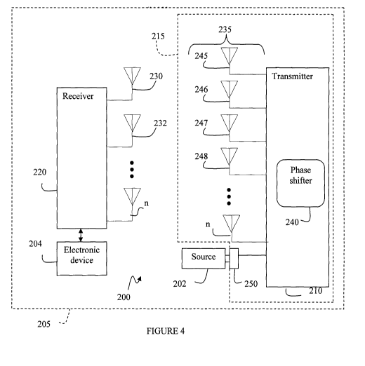
[0035] Reference is now made to Figure 4, which is a block
diagram of a system 200 for providing wireless RF power from a
source 202 to an electronic device 204 in a bounded area 205
according to an embodiment. The source 202 can be a main building
electrical circuit or any type of other power such as battery
source. The electronic device 204 may be any small device such as
sensors to detect, for example, movement, temperature, humidity,
etc. The device 204 may comprise actuators like switches, relays,
solenoids and motors. The device 204 can also be a remote
control, a clock, a smoke detector, an intrusion detection, etc.
The system 200 can be any electrical system such as an
aeronautical system, an automobile system, a cellular system, an
office in a commercial building, a room in a residential
building, etc, where transmitters are used as controllers to
transmit wireless RF power to a receiver of an electronic device.
[0036] The system 200 comprises a transmitter 210 for
transmitting RF power to a receiver 220. The transmitter 210 and
the receiver 220 comprise radiating elements 230, 232 and 245-
6
CA 02785446 2012-06-22
WO 2011/075819 PCT/CA2010/001962
05202939-2PCT
248. The radiating elements 245-248 can also be referred to as
ferromagnetic RF antennae. The area 205 can be any vehicle, room
or other open area that may comprise nulls and reflecting points
that cause the RF power signal sent from the transmitter 210 to
the receiver 220 to be altered or blocked, and thus causing loss
of RF power.
[0037] The transmitter 210 can be any device for intentionally
generating RF waves of RF power. The transmitter 210 can be a
communication device capable of two-way communication with the
receiver 220. The transmitter 210 may use known wireless
technologies such as Zigbee, Wi-Fi, and Bluetooth to provide, for
example, redundancy check, data transmission and seamless
integration with communication networks such as Internet,
computer networks, Local Area Networks (LANs), Wide Area Networks
(WANs), Metropolitan Area Networks (MANs) and others. Using
phased array technologies can allow the transmitter 210 to aim a
beam towards a required location to optimize radio transmission
and reception.
[0038] Figure 4 shows a phased array antenna 235 mounted to
the transmitter 210. The combination of the phased array antenna
235 and the transmitter 210 constitutes a remote device powering
module 215. The phased array antenna 235 comprises radiating
elements 245-248 for transmitting RF power from the source 102
via the transmitter to the receiver 220, and a plurality of
radiating elements can be part of the phased array antenna 235.
[0039] The transmitter 210 comprises a phase shifter module
240 for shifting the phase of a signal which is then fed to the
antennae. The phase shifter module 240 allows radiation emitted
from the antennae to produce a radiated pattern, which causes
constructive radiation intensity in desired direction and
destructive radiation intensity in undesired direction. The phase
shifter module 240 is a combination of hardware and software
7
CA 02785446 2012-06-22
WO 2011/075819 PCT/CA2010/001962
05202939-2PCT
parts that calculate a phase shift increment icp between radiating
elements of the phased array antenna 235 that are neighbors. For
example, it would be possible to determine the Acp between
radiating element 245 and radiating element 246, between
radiating element 247 and radiating element 248, etc. In another
embodiment, the phase shifter module 240 can also be manually or
automatically modified to obtain the phase shift increment Lcp
between two neighboring radiating elements.
[0040] Reference is now made to Figure SA, which is a block
diagram of a transmitter 210 equipped with the phase shifter
module 240 in accordance with an embodiment. The transmitter 210
comprises a connector 250 for providing an electrical connection
with the source 202. The connector 250 may be any electrical plug
adaptor, a battery adaptor, or any other type of connector
allowing contact between the power source 202 and the transmitter
210. The power is transmitted from the power source 202 via the
connector 250 to a conversion circuit 260. The conversion circuit
260 allows the conversion of the power to an electrical signal.
The transmitter 210 comprises a synthesizer 310, which can be any
device that creates a waveform such as an oscillator. In the
illustrated example, the synthesizer 310 generates a frequency to
be applied to the electrical signal where the frequency is
digitally controlled based on a value of reference 305. The
electrical signal is then shifted by the phase shifter module
240. After being shifted by the phase shifter module 240, the
electrical signal is amplified by the power amplifiers 325 and
transmitted by the radiating elements 245-248 as RF power via RF
waves.
[0041] In another embodiment, the phase shifter module 240 can
shift the phase from the reference phase before it is sent to the
synthesizer 310. As illustrated in Figure 5B, which is a variant
of the transmitter 210, a transmitter 211 uses a synthesizer 310
8
CA 02785446 2012-06-22
WO 2011/075819 PCT/CA2010/001962
05202939-2PCT
for each one of radiating elements 245-248, and the phase shifter
240 is then located before the synthesizer 310 to shift the
phase.
[0042] In the embodiments of Figures 5A and 5B, the beam
resulting from the radiating elements, at least one of which
emits a signal that is shifted in phase, is wider than a beam
obtained with radiating elements where the emitted signals have
the same phase. Furthermore, in Figures 5A and 5B there is shown
only one phase shifter module 240, but it is understood that the
signal provided to each one of the radiating elements can be
shifted with a desired phase shift increment (i(p). Alternatively,
when the transmitter comprises more than two radiating elements,
the AT can be determined for two consecutive or non consecutive
radiating elements, as it is described below.
[0043] Reference is now made to Figure 6A, which is a diagram
representing the RF signal emitted by two radiating elements 245,
246. In Figure 6A, each of the radiating elements 245, 246 is fed
with an electrical signal having the same phase. The
electromagnetic signal is amplified by constructive interference
in the main direction to obtain a beam 400.
[0044] Referring now to Figure 6B, there is shown a beam 405
of a dipole of antennae where radiating element 246 has a phase
shifted with respect to radiating element 245, which causes the
beam 405 to be shifted upward and to be wider than the beam 400.
Therefore, the beam 405 can avoid nulls and dead spots that may
otherwise be present in the bounded area 205.
[0045] Referring now to Figure 6C, there is shown a beam 410
of a pair of dipole antennae, where radiating elements 245 and
246 may each be a dipole antenna. In this embodiment, the beam
410 is directed by the radiating dipole antennae in a specific
direction. In this embodiment, the paths of the RF power signal
9
CA 02785446 2012-06-22
WO 2011/075819 PCT/CA2010/001962
05202939-2PCT
are altered and cause constructive reflections and may reduce the
presence of nulls. This may increase the RF power signal
intensity at the receiver location and may eliminate RF power
signal loss due to reflection. Therefore, as indicated above for
beam 405, beam 410 can avoid nulls and dead spots that may
otherwise be present in the bounded area 205.
[0046] The equation below refers to isotropic radiating
elements. The isotropic radiating element is an energy source
that radiates uniformly in all direction. The following equation
provides the phase shift cp between radiating elements:
cp = (3 60/A) * (d *sin(9s) (2)
Where:
d = distance between the radiating elements
6s= beam steering
A = wavelength
[0047] Referring now to Figure 7, there is shown an example of
a shifted phase and the application of the equations listed
above. In this example, the distance d is 0.05m and the
wavelength A is 0.33m. The curve 505 represents the phase shift
of the variation of the electrical signal versus the beam
steering in degrees between the radiating elements 245, 246.
[0048] Reference is now made to Figure 8, which is a schematic
illustrating a frequency scanning array configuration. In one
embodiment, the beam steering is obtained by changing the phases
of the electrical signals provided to the radiating elements.
Radiating elements 345, 346 are found at the end of a folded
waveguide 615, which acts as a delay line. The transmitter 602
generates a signal, which is sent at a desired frequency through
the folded waveguide 615 to radiating elements 345, 346. The
CA 02785446 2012-06-22
WO 2011/075819 PCT/CA2010/001962
05202939-2PCT
folded waveguide 615 shifts the phase of the electrical signal
sent to radiating element 346, and beam steering is done
proportionally to the transmitted signals (sin(t) and sin(to)) of
radiating elements 345, 346. Thus a greater time delay will cause
a greater change of the phase of the signal. In another
embodiment, the frequency scanning array may comprise more than
two radiating elements. In that case, each additional radiating
element may be connected to the transmitter 602 through a
corresponding waveguide. Doing this adds a cumulative delay to
for each added radiating element.
[0049] Figures 9A-9D are graphical representations of shifted
phases using the frequency scanning array of Figure 8 in
accordance with an embodiment. The Figures 9A-9D show different
examples of curves of the electrical signal transmitted to the
radiating elements 345 and 346 with different values of
frequencies used. In these figures, the RF power curves are
obtained using:
Vref(t) = Sin [2TTft] (3)
V2(t) = sin [21Tf* (t + to) ] (4)
[0050] In another embodiment of the transmitter 210, the phase
shifter module 240 can be a vector modulator. Reference is now
made to Figure 10, which is a block diagram of a vector modulator
800 in accordance with an embodiment. The vector modulator 800
comprises a divider 805, a summer 810, and converters 815.
[0051] A signal 0(t), which is the reference value of the
phase of the RF signal is provided to the divider 805. 0 (t) is
given by,
11
CA 02785446 2012-06-22
WO 2011/075819 PCT/CA2010/001962
05202939-2PCT
0(t) = sin(2irFr 360) (5 )
Where:
t = time in seconds
Fr = frequency of the local oscillator
[0052] The phase of 9(t) is then shifted with the divider
805 to obtain 9'(t). The shifted signal 9'(t) is given by:
s i n (6)
[0053] The converters 815 convert the shifted signal 9' (t)
with input signal Vl(x) to converted signal a(t,x) and the
original signal 9(t) with V2(x) to converted signal c(t,x).
Vl(x), V2(x), a(t,x) and (D(t,x) are given by,
V1(x) = Ao sin( 360, x) (6) 2 V2(x)=Aocos 360, x) (7)
a(t, x) = V1(x)9' (t) = Ao sin 360, x) sin2,rFr 360 + 2 ) (8)
O(t, x) = V2(x)O(t) = A,, cos 360' x) sin(2nFr 360) (9)
where:
A0 = magnitude
12
CA 02785446 2012-06-22
WO 2011/075819 PCT/CA2010/001962
05202939-2PCT
x = time in seconds of the input signals
t = time in seconds of the reference signal
[0054] The converted signals a(t,x) and (D(t,x) are combined
with the summer 810 into output signal i4r(t,x), which is provided
to antennae 245-248. The output signal is given by,
yr(t,x) = a(t,x)+q'(t,x) (10)
[0055] Reference is now made to Figure 11, which is a
graphical representation of shifted phases using the vector
modulator 800 in accordance with an embodiment.
[0056] In another embodiment of the transmitter 210, the phase
shifter module 240 can be a digital control phase shifter, a
linear control phase shifter, a load line phase shifter, a
ferroelectric phase shifter, a reflective phase shifter, a
Schiffman phase shifter, etc, and can be used in the context of
Figure 5A. Reference is now made to Figures 12A-12C, which are
schematic diagrams of phase shifter modules in accordance with
various embodiments. These phase shifter modules allow the beam
to be wider than a beam without a shifted signal. The RF power
of a wider beam can then be transmitted even when nulls or dead
points are present in the bounded area 205.
[0057] In the embodiment of Figure 12A, the digitally
controlled phase shifter consists of a series of delay line
circuits 821, which can be switched on/off by a digital control
822. Each delay line circuit 821 can be implemented by a
conventional coaxial line. In another embodiment, a micro strip
delay line or a lump element such as an inductor capacitor delay
line can be used. In another embodiment, a linear control phase
shifter using a delay line circuit can be used. The delay line
circuit shifts the phase of the signal transmitted to a radiating
element. In the embodiment of Figure 12B, there is shown a linear
13
CA 02785446 2012-06-22
WO 2011/075819 PCT/CA2010/001962
05202939-2PCT
control phase shifter using a high pass delay line circuit 830.
In Figure 12B, the high pass delay line 830 comprises a series of
high pass filters 831. In the embodiment of Figure 12C, there is
shown a linear control phase shifter using a low pass delay line
circuit 840. In Figure 12C, the low pass delay line 840 comprises
a series of low pass filters 841.
[0058] Referring back to Figures 5A and 5B, the RF power
transmitted by the transmitters 210, 211 is detected by the
receiver 220 and conversion to DC voltage occurs. Reference is
now made to Figure 13, which is a block diagram of the receiver
220 in accordance with an embodiment. The receiver 220 can be any
device such as a tuner for RF power, a communication device
capable of two-way communication with the transmitter 210 using
known spread spectrum technologies, etc. The receiver 220
comprises receiving antennae up to n receiving antennae for
receiving the RF power, a matching network 905 for transmitting
the RF AC voltage to a detector 910. The detector 910 then
converts the received RF power to DC voltage.
[0059] The dimension and radiated resistance of a receiving
antenna are among the parameters which affect the overall
performance of the receiver 220. The dimensions are governed
mainly by the operating frequency, and the radiated resistance
(antenna impedance) will determine the voltage generated by the
antenna for a given received RF power. The following formula
provides the voltage received by a receiving antenna such as
receiving antenna 230.
V - ~ O dBmisolropic +CIB~,in
r IOOO (11)
Where:
dBmisotropic = power received by an isotropic antenna
14
CA 02785446 2012-06-22
WO 2011/075819 PCT/CA2010/001962
05202939-2PCT
dBGain = gain of the antenna used
Rr = radiated resistance of the antenna
[0060] Reference is now made to Figures 14A,14B,14C and 14D,
which are schematic diagrams of antennae that can be used with
the receiver 220 for power harvesting in accordance with an
embodiment. Figure 14A illustrates a patch antenna, figure 14B
illustrates a circular patch antenna, figure 14C illustrates a
micro-strip slot antenna, and figure 14D illustrates a micro-
strip dipole antenna. Other types of antennae may also be used,
as will be understood by the person skilled in the art.
[0061] Reference is now made to Figure 15, which is a
schematic diagram of an RF detector 910 in accordance with an
embodiment. As discussed above the RF detector 910 converts the
received RF power to DC voltage. The RF power is received as RF
Alternative Current (AC) and is converted to DC voltage using a
diode 911. After voltage conversion by the RF detector 910, the
voltage can be increased with a voltage multiplier. The voltage
multiplier receives AC voltage, and converts AC voltage to DC
voltage.
[0062] Referring to Figure 16A a voltage multiplier 930
comprises a positive configuration of diodes 931, 932. The
voltage multiplier 930 uses the positive configuration of diodes
931, 932 to provide a positive voltage.
[0063] Referring to Figure 16B, a voltage multiplier 940
comprises a negative configuration of diodes 931, 932. The
voltage multiplier 940 uses the negative configuration of diodes
931, 932 to provide a negative voltage.
[0064] Referring to Figure 16C, an RF voltage quadrupler
detector 950, which comprises a positive configuration of four
diodes to provide a positive voltage. Alternatively, the RF
CA 02785446 2012-06-22
WO 2011/075819 PCT/CA2010/001962
05202939-2PCT
Voltage Quadrupler detector 950 can comprise a negative
configuration of diodes to provide a negative voltage. The
negative configuration is obtained by reversing the direction of
each diode.
[0065] Reference is now made to Figure 17, which is a flow
chart of a method for providing power from the source 202 to the
electronic device 204 located in the bounded area 205. According
to 1005, the power received from the source 202 is converted to
an electrical signal. According to 1007, a waveform is
generated. The reference frequency provides the reference phase.
According to 1010, the phase is shifted before the signal is
transmitted to one radiating element 245-248 of the phased array
antenna to generate a rotating beam. According to 1015, RF power
is transmitted by the phased array antenna 235 using RF waves.
According to 1020, the RF power is transmitted based on the
reference phase and the shifted phase. The reference phase and
the shifted phase allow the RF power to be sent to nulls and dead
points or portions of the bounded area 205 that cause reflection
of the RF power. According to 1025, the receiver converts RF
power to direct voltage at the receiver.
[0066] In another embodiment, the reference phase can be
shifted by a phase shifter module before it is sent to the
synthesizer 310. In an alternate embodiment, the method for
providing power from the source 202 to the electronic device 204
using low power levels may contribute to respect the exposure
limit of the human body to RF power.
[0067] The exposure limit to the human body is determined by
power density mw/cmz for a fixed duration. For 300 MHz to 1500
MHz, the exposure limit is fa/1500 mW/cmz where fo is the
frequency of transmitted energy emitted for a duration of 30
minutes on and 30 minutes off. For 900 MHz frequency band, the
exposure is 600 11W/cmz. If the power density is below 600 pW/cm2
16
CA 02785446 2012-06-22
WO 2011/075819 PCT/CA2010/001962
05202939-2PCT
then the emitted energy can be transmitted continuously. If duty
cycle radiated power is present, then the power density can be
calculated by,
I Sexp texp = `J Limit tavg (14)
Where:
Sexp = Power density Level of exposure (mW/cm2) = Power
density x Duty Cycle period (Exposure duration is for
example 30 minutes on/30 minutes off without regard to duty
cycle)
Siimit = Appropriate power density MPE limit (mW/cm2)
teXp = Allowable time of exposure for Sexp
tang = Appropriate Means Percent Error (MPE) averaging time
[00681 In yet another embodiment the method for providing
power from the source 202 to the electronic device 204 located in
the bounded area 205 may eliminate the use of batteries by
improving the reliability and costs of the system especially in
hard-to-reach location by eliminating the need for replacement of
batteries. This may also reduce the size and the weight of the
device 204 in applications such as in aeronautics where these
parameters are critical.
[00691 In an alternate embodiment, the method for providing
power from the source 202 to the electronic device 204 can
replace solar cells for locations where light is not available or
limited in time such as ceiling spaces in HVAC, closets in
buildings, etc.
17
CA 02785446 2012-06-22
WO 2011/075819 PCT/CA2010/001962
05202939-2PCT
[0070] In a further embodiment, the method for providing power
from the source 202 to the electronic device 204 may also
eliminate cabling in applications where the weight of cables and
related structures is inconvenient or where running cables and
drilling in walls is not recommended such as in museums,
historical buildings, etc. Furthermore, by removing a physical
link such as wires, it can be possible to ensure mobility of the
device 204. Then the device may not be restricted to a particular
location and may not need to be relocated, or can be relocated
easily.
[0071] In yet another embodiment, a phased array technique
permits to adapt power levels to changes in the environment. The
technique is used to overcome interference and nulls generated by
the introduction of elements and obstacles in the new
environment, thus avoiding the relocation of the transmitter 210
or the receiver 220 when changes in environment occur.
[0072] Those skilled in the art will understand that the
system 200 is not limited to the number of elements shown in
Figures 4 to 16. For example, the system 200 may comprise more
transmitters and receivers. More particularly, it should also be
understood that Figures 4 to 16 depict simplified hardware and
software parts, and that other hardware and software parts may
have been omitted for clarity reasons. Those skilled in the art
will understand that the hardware parts of the system 200 include
processors and electronic parts to execute the method described
above. Those skilled in the art will understand that the software
parts of the system 200 include instructions and computer code
that are executed by the processors and electronic parts to
modify the system 200, to generate RF power, to transmit RF power
using RF waves between an RF power source and an electronic
device, and to convert the RF power to DC voltage.
18
CA 02785446 2012-06-22
WO 2011/075819 PCT/CA2010/001962
05202939-2PCT
[00731 The embodiments described above are intended to be
exemplary only. The scope of the invention is therefore intended
to be limited solely by the scope of the appended claims.
19