Note: Descriptions are shown in the official language in which they were submitted.
CA 02785593 2015-11 -19
1
REDUNDANT MODULE WITH SYMMETRICAL CURRENT PATHS
The present invention relates to a redundant module for
decoupling short-circuit currents in a redundant voltage
supply.
In electrical systems, machines, or devices which are subject
to high requirements in terms of availability and reliability,
control and safety related functions are provided by redundant
voltage supplies. This redundancy is, for example, ensured by
at least two coupled power supply units which feed the
respective devices in parallel operation. The output power of
the individual power supply units is dimensioned such that at
least in case of failure of one of the power supply units, the
required electric power is provided by the remaining power
supply units.
The parallel-connected power supply units are routed to a
common current node at the output side, from which the total
electrical power provided is distributed to respective
consumers of a system, machine, or device. In order for the
common current node, in the event of a short-circuit at the
output side in any of the power supply units which could occur
as a result of a defect in the power supply unit, to be not
loaded by the resulting short-circuit current, it is necessary
for this case to decouple the power supply units from one
another. To this end, generally, so called redundant modules
are used which provide a separate input for each of the power
supply units to be connected in parallel, each of these inputs
being routed to a common output, via a decoupling diode. Such
CA 02785593 2015-11-19
2
a circuit, also known as an 0-ring circuit, decouples a short-
circuited power supply unit from the common current node at
the output of the redundant module, into which node in normal
operation all parallel power supply units feed its output
current. If, for example, in a short-circuit event the output
voltage of a power supply unit drops to zero potential, the
result is a negative voltage drop between the corresponding
input and the current node at the output of the redundant
module, so that the decoupling diode blocks a possible short-
circuit current.
In order to have a lowest possible power dissipation at the
decoupling diodes in normal operation, a redundant module
typically uses Schottky diodes which exhibit a low forward
voltage of about 400 mV. Corresponding redundant modules are
also known in form of so-called 0-ring diodes as integrated
devices.
A disadvantage of the known redundant modules is that the
parallel operated redundant power supply units are unevenly
loaded when feeding into the common current node, which
shortens the operating life of individual power supply units.
Another disadvantage of known redundant modules is that the
operability of the decoupling diodes and the presence of
redundancy cannot be monitored.
Embodiments of the present disclosure provide a redundant
voltage supply with at least two power supply units, which
significantly increases the availability of systems, machines,
or devices, and which in particular avoids the disadvantages
mentioned above.
CA 02785593 2015-11 -19
3
Particular embodiments provide a redundant module for
decoupling short-circuit currents in a redundant voltage
supply having at least two power supply units.
The redundant module has a number of inputs which is at least
equal to the number of power supply units, and each input is
routed via a separate current path to a common current node of
an output for providing an output current, and each of the
current paths forms a decoupling section. Each decoupling
section has at least one measuring element associated
therewith, for measuring the input voltage, the input current,
and/or the input power, and a control element for regulation
purposes.
Such a redundant module allows advantageous regulation of the
path currents and voltage drops of each decoupling section.
The measuring elements and control elements may be connected
to a control and regulation device which is adapted to
regulate the current, voltage, and/or power.
Embodiments provide a redundant module with active decoupling
sections which allow regulation of the currents in the current
paths between the respective number of inputs and the common
current node at the output of the redundant module, so that
the total current that is provided at the output of the
redundant module can be distributed symmetrically into equal
path currents, or can be distributed into predefined different
path currents.
4
Certain exemplary embodiments can provide a redundant module
for decoupling short-circuit currents in a redundant voltage
supply, comprising: at least two power supply units, a number
of inputs which corresponds at least to a number of power
supply units, and a control device, wherein each input is
routed via a separate current path to a common current node of
an output for providing an output current, each current path
forms a decoupling section, each decoupling section comprising
at least one measuring element for measuring input voltage,
path current flowing through the current path, and/or input
power, and a control element, and wherein the control device
is connected with the control element of each current path to
control a balance of path currents by i) adjusting a control
element of a first current path with a lowest positive input
voltage to a minimum resistance value, and ii) setting a
control element of a second current path as the active control
element, the current of the first path defining the target
value for controlling the current of the second current path.
Certain exemplary embodiments can provide a method for
providing a redundant voltage supply having at least two power
supply units and a redundant module as described herein,
comprising the steps of: (a) determining the input voltages
applied at the decoupling sections; (b) disabling the control
elements in those decoupling sections, at which no voltage is
applied; (c) adjusting the control element in the decoupling
section at which the lowest positive input voltage is provided
to a minimum resistance value; (d) determining current,
voltage, and/or power measurement data in all decoupling
sections; (e) controlling the control element of the at least
one further decoupling section, wherein the measured value of
CA 2735593 2017-07-04
5
. the decoupling section at which the lowest input voltage is
applied is determined as the target value for said
controlling.
The control and regulation device may be implemented, for
example, in a microcontroller which comprises digital-to-analog
converters for driving the control elements and acquiring
measurement data.
The control and regulation device may be adapted to distribute
the output current symmetrically or into currents with defined
ratios.
The control element may comprise a MOSFET, and the measuring
element may comprise a measuring resistor, wherein the MOSFET
and the measuring resistor are connected in series in the
current path of the decoupling section.
A measuring resistor which is connected in series with a MOSFET
in a decoupling section can determine the current flowing
through the current path of a decoupling section from the
voltage drop, which current serves as a parameter for current
regulation. Advantageously, with such a current measurement a
low resistance measuring resistor can be used as a measuring
element in the current path, so that power dissipation in the
decoupling section is low.
As an alternative to an ohmic measuring resistor, a diode
connected in series with the MOSFET can be used to sense the
path current in the decoupling section. Also, inductive
current measurement is possible.
CA 2735593 2017-07-04
CA 02785593 2015-11-19
6
Instead of current measurement, it is within the scope of the
invention to detect the voltage at the output of each control
element, so that the control element may be voltage-
controlled.
Generally, other controllable semiconductor components are
also suitable as control elements, such as IGBTs, or bipolar
transistors.
In the redundant module, a diode may be connected in parallel
to the MOSFET of each decoupling section to protect the
transistor from overcurrents which might be caused for example
by a short-circuit at the output of the redundant module.
Preferably, the measuring element of each decoupling section
may have a sense amplifier associated therewith. The sense
amplifier can detect very low voltage differences at the
measuring resistance and process them for the control and
regulation device. This allows the use of extremely low-
resistance measurement resistors, for further reduction of
power dissipation in a decoupling section.
The decoupling sections may additionally include measuring
elements for monitoring the temperature and the input voltage,
which elements are connected to the regulation device. The
decoupling sections may thus be monitored by the control and
regulation device.
Due to its regulation device, the redundant module is adapted
to detect a failure or a short-circuit of a power supply unit
at the input of each decoupling section, and to switch off an
CA 02785593 2015-11-19
7
affected current path by blocking the transistor in the
respective current path.
Due to such active decoupling of short-circuits at the input
side, the present invention allows a decoupling diode in the
respective current paths to be eliminated.
Of course, instead of active decoupling, decoupling of short-
circuit currents using a Schottky diode may still be provided.
The control and regulation device of a redundant module may
comprise a number of digital and/or analog interfaces adapted
for diagnosis, programming, and parameterization, as well as
for communication with other control and regulation devices of
a system, machine or device.
Thus, for example, failures of individual redundant power
supply units or an imminent thermal overload of a decoupling
section can be signaled, so that a system, machine, or device
can be brought into a safe state, if necessary.
A reduhdanL module may have at leasL a second redundant_ module
connected in parallel to the output, the parallel-connected
redundant modules being adapted to communicate with each other
and to provide a common control for a symmetrical or
predefined current distribution to all decoupling sections.
Thus, the invention provides for a distributed redundant power
supply through a common bus bar or power line, while enabling
symmetrical distribution of the currents, or power,
respectively, to all power supply units, due to the
CA 02785593 2015-11-19
8
communication of the control and regulation devices. This is
particularly advantageous when retrofitting additional power
supply units.
The invention further comprises a method for providing a
redundant voltage supply having at least two power supply
units and a redundant module according to the invention,
comprising the steps of:
(a) determining the input voltages applied at the decoupling
sections;
(b) disabling the control elements in those decoupling
sections, at which no voltage is applied;
(c) determining the decoupling section which has the lowest
positive input voltage applied at its input;
(d) adjusting the control element in the current path of the
decoupling section at which the lowest positive input
voltage is provided to a minimum resistance value;
(e) determining path current, voltage, and/or power
measurement data in all decoupling sections;
(f) regulating the control elements of the at least one
further decoupling section, wherein the measured value of
the decoupling section at which the lowest input voltage
is applied is determined as the target value for a
respective regulation.
The control element may be regulated in function of the
current flowing through the decoupling section.
The absolute amount of current in each of the regulated
current paths results from the total current flowing through
the output to the connected load.
CA 02785593 2015-11-19
9
The current path of the decoupling section at which the lowest
input voltage is detected is not regulated, so that the
corresponding path current can be supplied as a reference
value for the target value of each regulation of the at least
one further current path. By regulating the deviations, a
balance of currents among the paths is established.
Alternatively, the control element is regulated in function of
its output voltage.
The method allows to continuously monitor the input voltages
at the inputs of the redundant module, so that in case of
failure or short-circuit of a power supply unit the associated
decoupling section is cut off. In this way it can be removed
from the regulation scheme, so that the system, machine, or
device maintains its power supply through the power supply
units remaining in the regulation scheme.
The invention will now be described in detail with reference
to exemplary embodiments and to the accompanying drawings,
wherein:
Fig. 1 shows the operation of a redundant module having two
decoupling sections with variable resistors;
Fig. 2 shows a first embodiment of a redundant module having
two parallel-connected decoupling sections each
including a decoupling diode and a controllable or
regulatable MOSFET;
Fig. 3 shows a second embodiment of a redundant module having
two decoupling sections, with a diode connected in
parallel to each of the MOSFETs;
10
, Fig. 4 shows a third preferred embodiment of a redundant
module having two decoupling sections with controllable
or regulatable MOSFETs and without decoupling diodes
connected in series;
Fig. 5 shows a complete redundant module having two parallel
operating decoupling sections and a control and
regulation unit.
With reference to Fig. 1, the operation of a redundant module
with two decoupling sections will be explained. Two power
supply units, not shown in the figure, are connected to the
inputs IN1 and IN2 of the redundant module on the secondary
side thereof, and provide voltages Ul and U2 at the inputs of
the current paths. A load, likewise not shown in the figure,
which is to be powered by the redundant module can be connected
to the output OUT of the circuit. The output forms a common
current node for the outputs of the current paths of all
decoupling sections. The reference potential GND is connected
to the corresponding terminals of the power supply units.
Diodes D1 and D2 are decoupling diodes which are intended to
prevent, in the event of a short-circuit of an input, a return
current from the output OUT of the redundant module to the
short-circuited input.
Variable resistors R11 and R21 are exemplary control elements
of the control circuits by means of which the balance of
currents among the current paths of the supplying power supply
units can be regulated. The path currents are each measured by
a respective measuring resistor, R1 and R2.
CA 2735593 2017-07-04
CA 02785593 2015-11-19
11
To regulate the balance of currents, the variable resistor of
a first current path, that is the current path which has the
lower input voltage applied at its input, is adjusted to the
minimum resistance value. The variable resistor in a second
current path, i.e. the other one of the two illustrated
current paths, is the active control element of a regulation
scheme which regulates the balance of currents. The sensed
current data of the two current paths are supplied to a
regulation device, the current of the path with the lower
input voltage defining the target value for regulation of the
second current path.
In function of the deviation to be regulated which results
from the difference between the first and second path
currents, the value of the active, variable resistor in the
second current path is varied until both currents are
equalized. The regulation process always influences both path
currents, since the sum of the two path currents results from
the total current at the output of the circuit which depends
on the connected load and is constant in time, at least over
periods.
The present invention allows parallel operation of three or
more power supply units, by respectively defining the path
current of the decoupling section to which the power supply
unit with the smallest output voltage is connected as the
target value of the control circuits for the other current
paths. Since the sum of all path currents is defined by the
load at the output, all current paths are balanced to each
other with a symmetrical current load.
CA 02785593 2015-11-19
12
Fig. 2 illustrates a first embodiment of two parallel
decoupling sections. Diodes D1 and D2 are preferably provided
in form of SchoLLky diodes which are distinguished by a low
forward voltage of about 400 mV and thus produce lower power
losses in the current paths as compared to silicon diodes. The
variable resistors are shown as MOS transistors Ti and T2
operating in the linear regime. A circuit as illustrated
allows to even out significant differences in the output
voltages of the connected power supply units.
Fig. 3 shows another embodiment of a redundant module having
two decoupling sections connected in parallel. In contrast to
the illustration in Fig. 2, transistors Ti and T2 additionally
have a respective diode, Dll and D21, connected in parallel
thereto. These serve to protect against overcurrents, e.g. in
the event of a short-circuit at the output of the redundant
module. Once the voltage that drops between drain and source
of the MOSFET exceeds the forward voltage of a respective
diode, the latter may accommodate the path current and protect
the transistor from breakthrough. Preferably, Schottky diodes
are used as diodes Dll and D21. In this case, voltage
differences in the power supply units of up to 400 mV can be
compensated by regulating the path currents.
Fig. 4 illustrates a parlicularly preferred embodiment with
Lwo parallel-connected decoupling sections for a redundant
module with symmetrically regulatable path currents. A
particular advantage of an inventive redundant module is that,
in principle, the decoupling diodes of conventional redundant
modules can be dispensed with. As will be described below, the
control and/or regulation device of an inventive redundant
CA 02785593 2015-11-19
13
module comprises means which allow to monitor the input
voltages. In the event of a short-circuit at the input side
occurring in one of the power supply units, for example, the
associaLed current path with the respective transistor can be
switched off, so that a return flow of the output current from
the current node is actively suppressed. Diodes D12 and D21
connected in parallel to the MOSFETs allow emergency operation
of the redundant module in case of a failure of the regulation
device and/or the transistors.
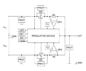
Fig. 5 shows a complete redundant module having two parallel
operating decoupling sections and a control and regulation
device connected to these modules. The regulation device is
implemented, for example, by a microcontroller device and
associated peripherals, and provides, in addition to the
current regulation regime for the current paths, numerous
input/output interfaces. These include, for example, the
light-emitting diodes LED which are used for diagnostic
purposes and to display operating modes, warnings, alarms, and
errors, control elements CNT, e.g. for setting an operating
mode, or digital outputs DO which are implemented using relay
contacts or electronic drivers. Via the COMM interface, the
redundant module may communicate with higher-level controllers
of systems, devices, or machines.
The decoupling sections essentially correspond to those which
have been described above with reference to Fig. 4, each one
comprising a MOSFET, Ti and T2, respectively, with a Schottky
diode, D11 and D21, respectively, connected in parallel
thereto, and a low-impedance measuring resistor connected in
series. Each decoupling section has a temperature sensor
CA 02785593 2015-11-19
14
associated therewith which enables to monitor the MOSFETs for
diagnostic purposes. The measuring resistors each have a sense
amplifier, OR1 and 0P2, respectively, connected in parallel
thereto, for amplification of the sensed voltage difference,
which is linearly related to the respective path current
through the resistor.
At the input side, each decoupling section has a voltage tap
by which the input voltage of each current path can be
detected by the microcontroller of the regulation device.
Optionally, the inputs and the output of the redundant module
may be connected to a protection circuit PROT which, for
example, includes noise filters and/or overvoltage filters.
The transistors of the current paths may also be connected to
such protection circuits.
The two input voltages Ul and U2 are required for initiation
of the regulation for a symmetric current distribution to the
two redundant power supply units. To this end, first the
voltages provided by the power supply units are tapped at the
inputs of the redundant module and fed to the regulation
device.
Voltages Ul and U2 allow the regulation device to check the
operability of the connected power supply units. If any of the
voltages falls to the reference potential or at least below a
specified threshold value, the associated transistor in the
corresponding current path can be blocked. The regulation
device will not interpret this current path as the current
path with the lowest input voltage. The reference value for
CA 02785593 2015-11 -19
regulation is provided by the current path having the lowest
valid input voltage. If there only remains one current path
carrying the total current, all current paths with loss of
input voltage are switched off, and the control element of the
5 path that carries the current is set to a minimum resistance
value.